LM4863
Dual 2.2W Audio Amplifier Plus Stereo Headphone
Function
General Description
The LM4863 is a dual bridge-connected audio power ampli-
fier which, when connected to a 5V supply, will deliver 2.2W
to a 4
load (Note 1) or 2.5W to a 3 load (Note 2) with less
than 1.0% THD+N. In addition, the headphone input pin
allows the amplifiers to operate in single-ended mode when
driving stereo headphones.
Boomer audio power amplifiers were designed specifically to
provide high quality output power from a surface mount
package while requiring few external components. To sim-
plify audio system design, the LM4863 combines dual bridge
speaker amplifiers and stereo headphone amplifiers on one
chip.
The LM4863 features an externally controlled, low-power
consumption shutdown mode, a stereo headphone amplifier
mode, and thermal shutdown protection. It also utilizes cir-
cuitry to reduce "clicks and pops" during device turn-on.
Note 1: An LM4863MTE or LM4863LQ that has been properly mounted to
a circuit board will deliver 2.2W into 4
. The other package options for the
LM4863 will deliver 1.1W into 8
. See the Application Information sections
for further information concerning the LM4863MTE and LM4863LQ.
Note 2: An LM4863MTE or LM4863LQ that has been properly mounted to a
circuit board and forced-air cooled will deliver 2.5W into 3
.
Key Specifications
n
P
O
at 1% THD+N
n
LM4863LQ, 3
, 4 loads
2.5W(typ), 2.2W(typ)
n
LM4863MTE, 3
, 4 loads
2.5W(typ), 2.2W(typ)
n
LM4863MTE, 8
load
1.1W(typ)
n
LM4863, 8
1.1W(typ)
n
Single-ended mode THD+N at 75mW into
32
0.5%(max)
n
Shutdown current
0.7µA(typ)
n
Supply voltage range
2.0V to 5.5V
Features
n
Stereo headphone amplifier mode
n
"Click and pop" suppression circuitry
n
Unity-gain stable
n
Thermal shutdown protection circuitry
n
SOIC, DIP, TSSOP and exposed-DAP TSSOP and LLP
packages
Applications
n
Multimedia monitors
n
Portable and desktop computers
n
Portable televisions
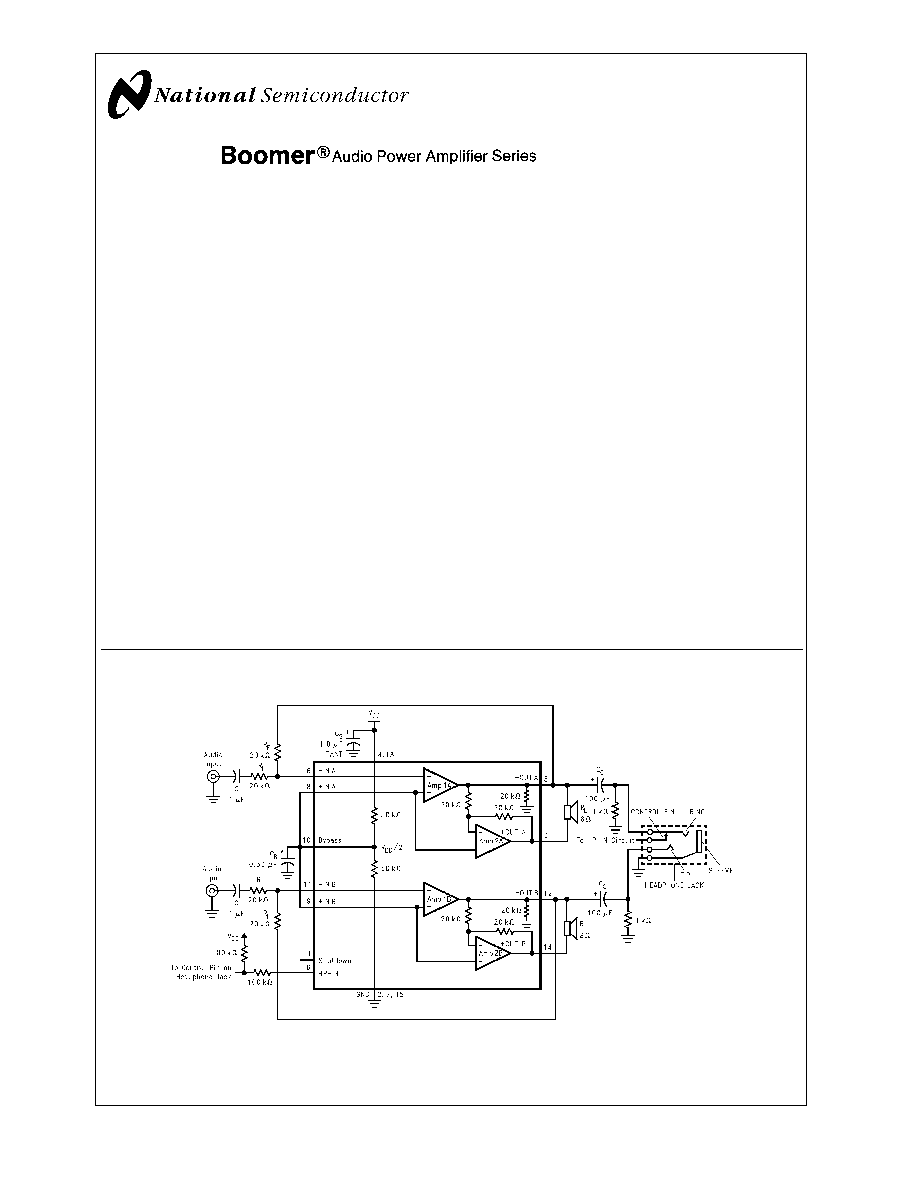
Typical Application
01288101
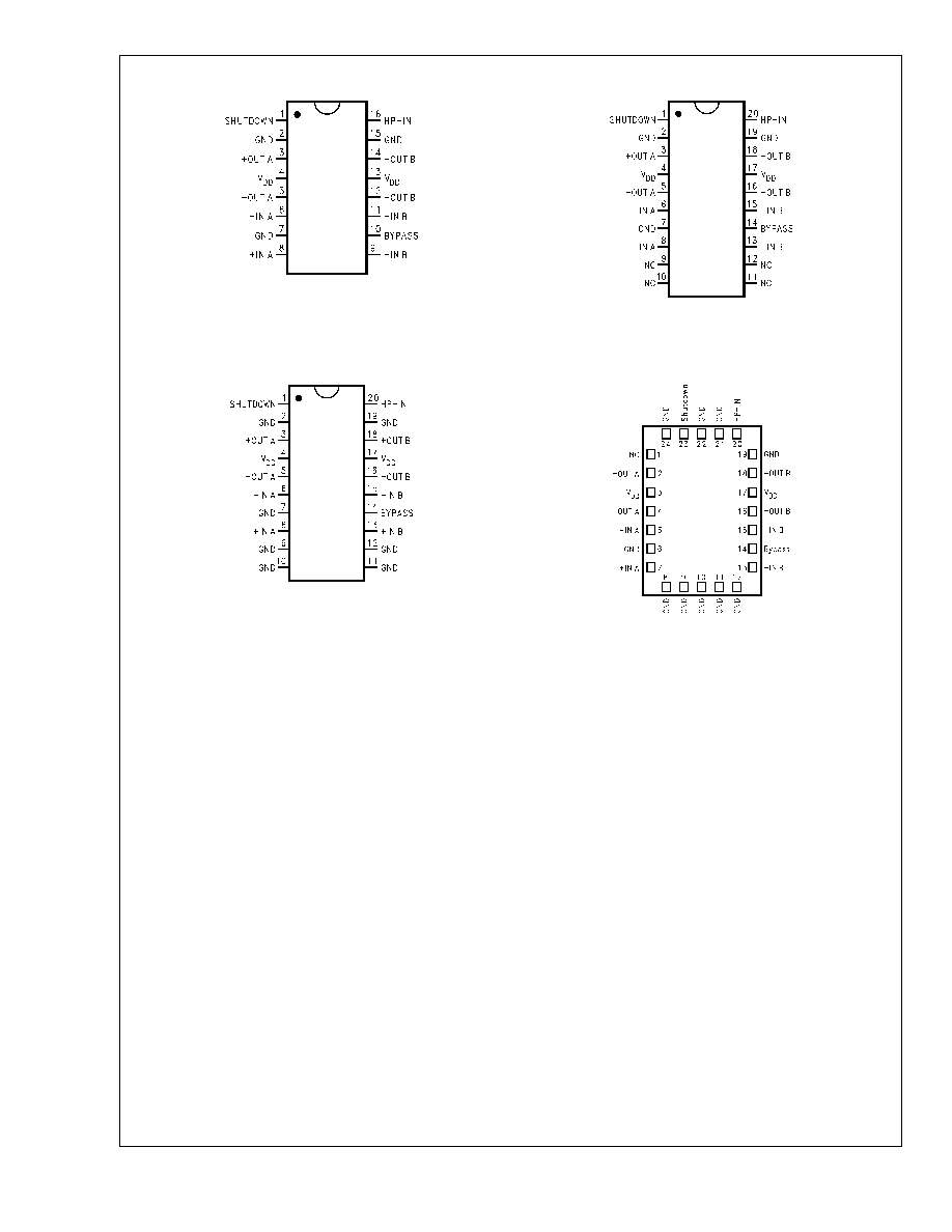
Note: Pin out shown for DIP and SO packages. Refer to the Connection Diagrams for the pinout of the TSSOP, Exposed-DAP TSSOP, and Exposed-DAP
LLP packages.
Boomer
Æ
is a registered trademark of National Semiconductor Corporation.
August 2002
LM4863
Dual
2.2W
Audio
Amplifier
Plus
Stereo
Headphone
Function
© 2002 National Semiconductor Corporation
DS012881
www.national.com
Absolute Maximum Ratings
(Note 3)
If Military/Aerospace specified devices are required,
please contact the National Semiconductor Sales Office/
Distributors for availability and specifications.
Supply Voltage
6.0V
Storage Temperature
-65∞C to +150∞C
Input Voltage
-0.3V to V
DD
+0.3V
Power Dissipation (Note 4)
Internally limited
ESD Susceptibility(Note 5)
2000V
ESD Susceptibility (Note 6)
200V
Junction Temperature
150∞C
Solder Information
Small Outline Package
Vapor Phase (60 sec.)
215∞C
Infrared (15 sec.)
220∞C
See AN-450 "Surface Mounting and their Effects on
Product Reliablilty" for other methods of soldering
surface mount devices.
Thermal Resistance
JC
(typ) -- M16B
20∞C/W
JA
(typ) -- M16B
80∞C/W
JC
(typ) -- N16A
20∞C/W
JA
(typ) -- N16A
63∞C/W
JC
(typ) -- MTC20
20∞C/W
JA
(typ) -- MTC20
80∞C/W
JC
(typ) -- MXA20A
2∞C/W
JA
(typ) -- MXA20A
41∞C/W (Note 7)
JA
(typ) -- MXA20A
51∞C/W (Note 8)
JA
(typ) -- MXA20A
90∞C/W(Note 9)
JC
(typ) -- LQ24A
3.0∞C/W
JA
(typ) -- LQ24A
42∞C/W (Note 10)
Operating Ratings
Temperature Range
T
MIN
T
A
T
MAX
-40∞C
T
A
85∞C
Supply Voltage
2.0V
V
DD
5.5V
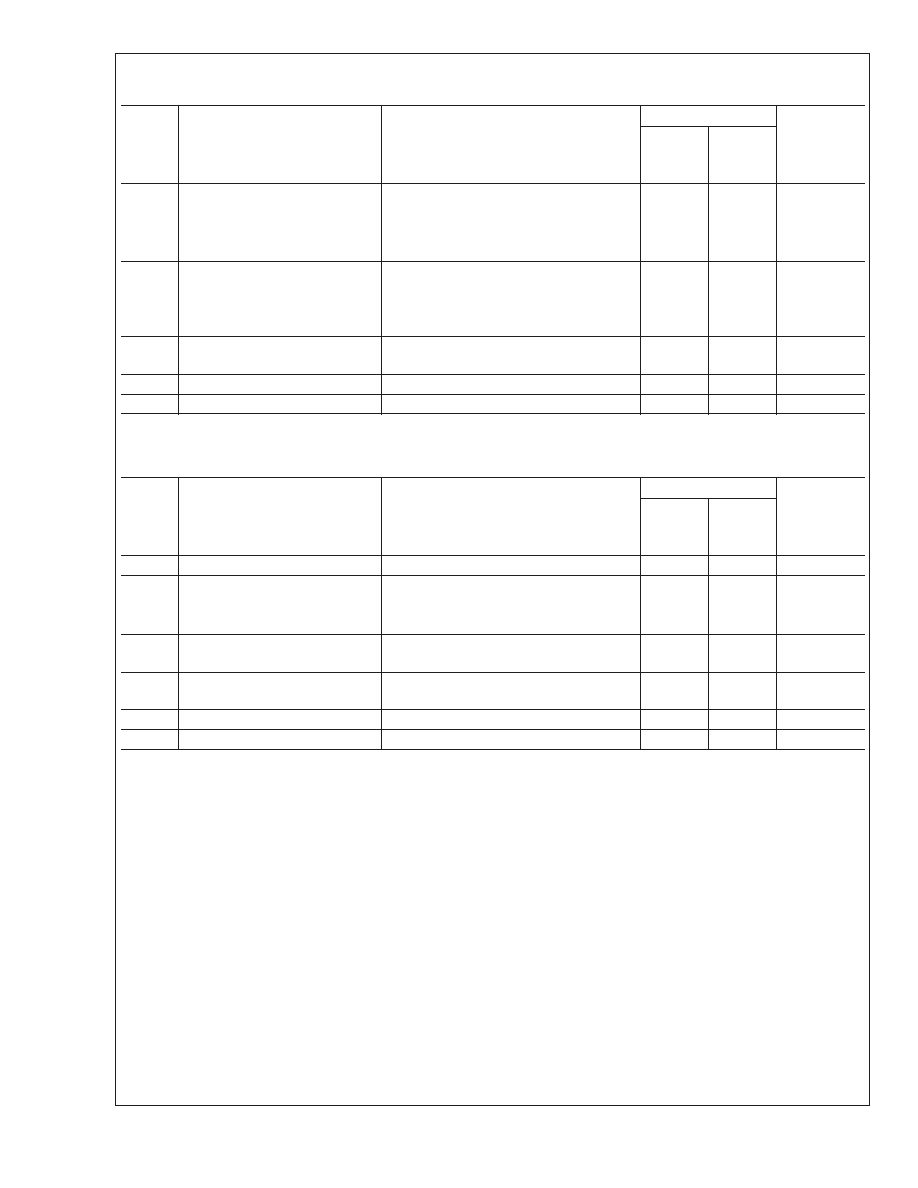
Electrical Characteristics for Entire IC
(Notes 3, 11)
The following specifications apply for V
DD
= 5V unless otherwise noted. Limits apply for T
A
= 25∞C.
Symbol
Parameter
Conditions
LM4863
Units
(Limits)
Typical
Limit
(Note 12)
(Note 13)
V
DD
Supply Voltage
2
V (min)
5.5
V (max)
I
DD
Quiescent Power Supply Current
V
IN
= 0V, I
O
= 0A (Note 14), HP-IN = 0V
11.5
20
mA (max)
6
mA (min)
V
IN
= 0V, I
O
= 0A (Note 14), HP-IN = 4V
5.8
mA
I
SD
Shutdown Current
V
DD
applied to the SHUTDOWN pin
0.7
2
µA (min)
V
IH
Headphone High Input Voltage
4
V (min)
V
IL
Headphone Low Input Voltage
0.8
V (max)
Electrical Characteristics for Bridged-Mode Operation
(Notes 3, 11)
The following specifications apply for V
DD
= 5V unless otherwise specified. Limits apply for T
A
= 25∞C.
Symbol
Parameter
Conditions
LM4863
Units
(Limits)
Typical
(Note 12)
Limit
(Note 13)
V
OS
Output Offset Voltage
V
IN
= 0V
5
50
mV (max)
P
O
Output Power (Note 15)
THD+N = 1%, f = 1kHz (Note 16)
LM4863MTE, R
L
= 3
LM4863LQ, R
L
= 3
2.5
2.5
W
W
LM4863MTE, R
L
= 4
LM4863LQ, R
L
= 4
2.2
2.2
W
W
LM4863, R
L
= 8
1.1
1.0
W (min)
THD+N = 10%, f = 1kHz (Note 16)
LM4863MTE, R
L
= 3
LM4863LQ, R
L
= 3
3.2
3.2
W
W
LM4863
www.national.com
3
Electrical Characteristics for Bridged-Mode Operation
(Notes 3, 11) (Continued)
The following specifications apply for V
DD
= 5V unless otherwise specified. Limits apply for T
A
= 25∞C.
Symbol
Parameter
Conditions
LM4863
Units
(Limits)
Typical
(Note 12)
Limit
(Note 13)
LM4863MTE, R
L
= 4
LM4863LQ, R
L
= 4
2.7
2.7
W
W
LM4863, R
L
= 8
1.5
W
THD+N = 1%, f = 1kHz, R
L
= 32
0.34
W
THD+N
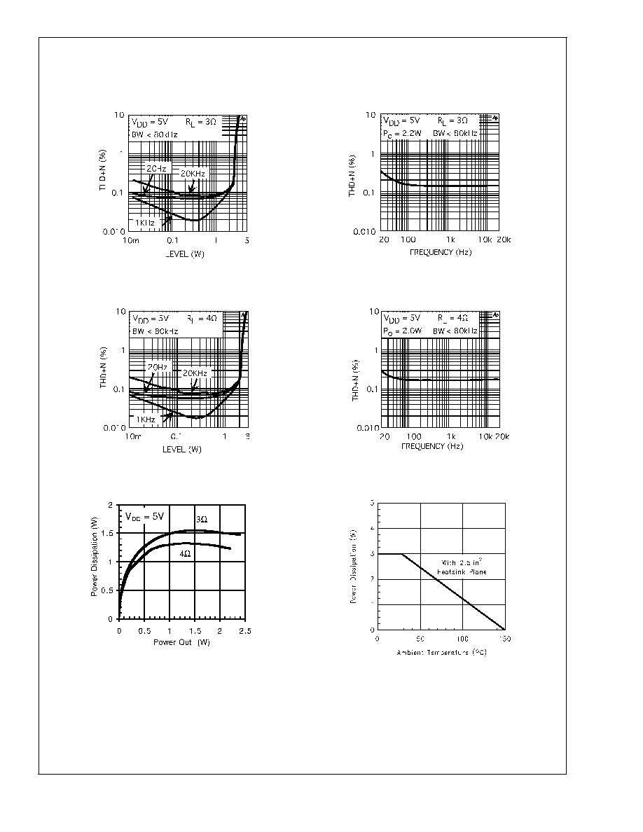
Total Harmonic Distortion+Noise
20Hz
f 20kHz, A
VD
= 2
LM4863MTE, R
L
= 4
, P
O
= 2W
LM4863LQ, R
L
= 4
, P
O
= 2W
0.3 0.3
%
LM4863, R
L
= 8
, P
O
= 1W
0.3
%
PSRR
Power Supply Rejection Ratio
V
DD
= 5V, V
RIPPLE
= 200mV
RMS
, R
L
= 8
,
C
B
= 1.0µF
67
dB
X
TALK
Channel Separation
f = 1kHz, C
B
= 1.0µF
90
dB
SNR
Signal To Noise Ratio
V
DD
= 5V, P
O
= 1.1W, R
L
= 8
98
dB
Electrical Characteristics for Single-Ended Operation
(Notes 3, 4)
The following specifications apply for V
DD
= 5V unless otherwise specified. Limits apply for T
A
= 25∞C.
Symbol
Parameter
Conditions
LM4863
Units
(Limits)
Typical
(Note 12)
Limit
(Note 13)
V
OS
Output Offset Voltage
V
IN
= 0V
5
50
mV (max)
P
O
Output Power
THD+N = 0.5%, f = 1kHz, R
L
= 32
85
75
mW (min)
THD+N = 1%, f = 1kHz, R
L
= 8
340
mW
THD+N = 10%, f = 1kHz, R
L
= 8
440
mW
THD+N
Total Harmonic Distortion+Noise
A
V
= -1, P
O
= 75mW, 20Hz
f 20kHz,
R
L
= 32
0.2
%
PSRR
Power Supply Rejection Ratio
C
B
= 1.0µF, V
RIPPLE
= 200mV
RMS
,
f = 1kHz
52
dB
X
TALK
Channel Separation
f = 1kHz, C
B
= 1.0µF
60
dB
SNR
Signal To Noise Ratio
V
DD
= 5V, P
O
= 340mW, R
L
= 8
95
dB
Note 3: Absolute Maximum Ratings indicate limits beyond which damage to the device may occur. Operating Ratings indicate conditions for which the device is
functional, but do not guarantee specific performance limits. Electrical Characteristics state DC and AC electrical specifications under particular test conditions which
guarantee specific performance limits. This assumes that the device is within the Operating Ratings. Specifications are not guaranteed for parameters where no limit
is given, however, the typical value is a good indication of device performance.
Note 4: The maximum power dissipation is dictated by T
JMAX
,
JA
, and the ambient temperature T
A
and must be derated at elevated temperatures. The maximum
allowable power dissipation is P
DMAX
= (T
JMAX
- T
A
)/
JA
. For the LM4863, T
JMAX
= 150∞C. For the
JA
s for different packages, please see the Application
Information section or the Absolute Maximum Ratings section.
Note 5: Human body model, 100 pF discharged through a 1.5 k
resistor.
Note 6: Machine model, 220 pF≠240 pF discharged through all pins.
Note 7: The given
JA
is for an LM4863 packaged in an MXA20A with the exposed-DAP soldered to an exposed 2in
2
area of 1oz printed circuit board copper.
Note 8: The given
JA
is for an LM4863 packaged in an MXA20A with the exposed-DAP soldered to an exposed 1in
2
area of 1oz printed circuit board copper.
Note 9: The given
JA
is for an LM4863 packaged in an MXA20A with the exposed-DAP not soldered to printed circuit board copper.
Note 10: The given
JA
is for an LM4863 packaged in an LQA24A with the exposed-DAP soldered to an exposed 2in
2
area of 1oz printed circuit board copper.
Note 11: All voltages are measured with respect to the ground (GND) pins unless otherwise specified.
Note 12: Typicals are measured at 25∞C and represent the parametric norm.
Note 13: Limits are guaranteed to National's AOQL (Average Outgoing Quality Level).
Note 14: The quiescent power supply current depends on the offset voltage when a practical load is connected to the amplifier.
Note 15: Output power is measured at the device terminals.
Note 16: When driving 3
or 4 and operating on a 5V supply, the LM4863LQ and LM4863MTE must be mounted to the circuit board that has a minimum of 2.5in
2
of exposed, uninterrupted copper area connected to the LLP package's exposed DAP.
LM4863
www.national.com
4