 | –≠–ª–µ–∫—Ç—Ä–æ–Ω–Ω—ã–π –∫–æ–º–ø–æ–Ω–µ–Ω—Ç: LM4864MM | –°–∫–∞—á–∞—Ç—å:  PDF PDF  ZIP ZIP |
LM4864
300 mW Audio Power Amplifier with Shutdown Mode
General Description
The LM4864 is a bridged audio power amplifier capable of
delivering 300 mW of continuous average power into an 8
load with 1% (THD) from a 5V power supply.
Boomer
Æ
audio power amplifiers were designed specifically
to provide high quality output power from a low supply volt-
age while requiring a minimal amount of external compo-
nents. Since the LM4864 does not require output coupling
capacitors, bootstrap capacitors or snubber networks, it is
optimally suited for low-power portable applications.
The LM4864 features an externally controlled, low power
consumption shutdown mode, and thermal shutdown protec-
tion.
The closed loop response of the unity-gain stable LM4864,
can be configured by external gain-setting resistors. The de-
vice is available in multiple package types to suit various ap-
plications.
Key Specifications
n
THD at 1 kHz at 300 mW continuous
average output power into 8
1.0% (max)
n
THD at 1 kHz at 300 mW continuous
average output power into 16
1.0% (max)
n
Shutdown current
0.7 µA (typ)
Features
n
MSOP, SOP, and DIP packaging
n
No output coupling capacitors, bootstrap capacitors, or
snubber circuits are necessary
n
Thermal shutdown protection circuitry
n
Unity-gain stable
n
External gain configuration capability
Applications
n
Cellular Phones
n
Personal Computers
n
General Purpose Audio
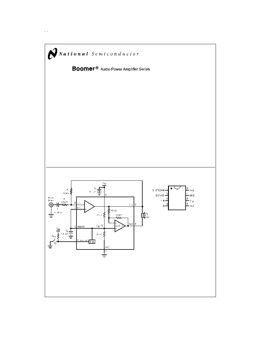
Typical Application
Connection Diagram
Boomer
Æ
is a registered trademark of National Semiconductor Corporation.
DS012607-1
FIGURE 1. Typical Audio Amplifier Application Circuit
MSOP, SOP, and DIP Package
DS012607-2
Top View
Order Number LM4864MM,
LM4864M or LM4864N
See NS Package Number MUA08A,
M08A or N08E
September 1999
LM4864
300
mW
Audio
Power
Amplifier
with
Shutdown
Mode
© 1999 National Semiconductor Corporation
DS012607
www.national.com
Absolute Maximum Ratings
(Note 2)
If Military/Aerospace specified devices are required,
please contact the National Semiconductor Sales Office/
Distributors for availability and specifications.
Supply Voltage
6.0V
Storage Temperature
-65∞C to +150∞C
Input Voltage
-0.3V to V
DD
+ 0.3V
Power Dissipation (Note 3)
Internally limited
ESD Susceptibility (Note 4)
3500V
ESD Susceptibility (Note 5)
250V
Junction Temperature
150∞C
Soldering Information
Small Outline Package
Vapor Phase (60 sec.)
215∞C
Infrared (15 sec.)
220∞C
See AN-450 "Surface Mounting and their Effects on
Product Reliability" for other methods of soldering surface
mount devices.
Thermal Resistance
JC
(MSOP)
56∞ C/W
JA
(MSOP)
210∞C/W
JC
(SOP)
35∞C/W
JA
(SOP)
170∞C/W
JC
(DIP)
37∞C/W
JA
(DIP)
107∞C/W
Operating Ratings
Temperature Range
T
MIN
T
A
T
MAX
-40∞C
T
A
+85∞C
Supply Voltage
2.7V
V
DD
5.5V
Electrical Characteristics
(Note 1) (Note 2)
The following specifications apply for V
DD
= 5V, for all available packages, unless otherwise specified. Limits apply for T
A
=
25∞C
Symbol
Parameter
Conditions
LM4864
Units
(Limits)
Typical
(Note 6)
Limit
(Note 7)
I
DD
Quiescent Power Supply Current
V
IN
= 0V, I
O
= 0A (Note 8)
3.6
6.0
mA (max)
I
SD
Shutdown Current
V
PIN1
= V
DD
0.7
5
µA (max)
V
OS
Output Offset Voltage
V
IN
= 0V
5
50
mV (max)
P
O
Output Power
THD = 1% (max); f = 1 kHz; R
L
= 8
;
LM4864MM (Note 9)
300
mW (min)
THD = 1% (max); f = 1 kHz; R
L
= 8
;
LM4864M and LM4864N
675
300
mW (min)
THD+N = 1%; f = 1 kHz; R
L
= 16
;
LM4864MM, LM4864M and LM4864N
550
mW
THD+N
Total Harmonic Distortion+Noise
P
O
= 300 mWrms; A
VD
= 2; R
L
= 8
;
20 Hz
f
20 kHz
0.7
%
PSRR
Power Supply Rejection Ratio
V
DD
= 4.9V≠5.1V
50
dB
Electrical Characteristics
(Note 1) (Note 2)
The following specifications apply for V
DD
= 3V, for all available packages, unless otherwise specified. Limits apply for T
A
=
25∞C
Symbol
Parameter
Conditions
LM4864
Units
(Limits)
Typical
(Note 6)
Limit
(Note 7)
I
DD
Quiescent Power Supply Current
V
IN
= 0V, I
O
= 0A (Note 8)
1.0
3.0
mA (max)
I
SD
Shutdown Current
V
PIN1
= V
DD
0.3
2.0
µA (max)
V
OS
Output Offset Voltage
V
IN
= 0V
5
mV
P
O
Output Power
THD = 1% (max); f = 1 kHz; R
L
= 8
200
mW
THD = 1% (max); f = 1 kHz; R
L
= 16
175
mW
THD+N
Total Harmonic Distortion+Noise
P
O
= 100 mWrms; A
VD
= 2; R
L
= 8
;
20 Hz
f
20 kHz, BW
<
80 kHz
1.5
%
PSRR
Power Supply Rejection Ratio
V
DD
= 2.9V≠3.1V
50
dB
Note 1: All voltages are measured with respect to the ground pin, unless otherwise specified.
Note 2: Absolute Maximum Ratings indicate limits beyond which damage to the device may occur. Operating Ratings indicate conditions for which the device is func-
tional, but do not guarantee specific performance limits. Electrical Characteristics state DC and AC electrical specifications under particular test conditions which guar-
antee specific performance limits. This assumes that the device is within the Operating Ratings. Specifications are not guaranteed for parameters where no limit is
given, however, the typical value is a good indication of device performance.
www.national.com
2

Electrical Characteristics
(Note 1) (Note 2) (Continued)
Note 3: The maximum power dissipation must be derated at elevated temperatures and is dictated by T
JMAX
,
JA
, and the ambient temperature T
A
. The maximum
allowable power dissipation is P
DMAX
= (T
JMAX
- T
A
)/
JA
or the number given in the Absolute Maximum Ratings, whichever is lower. For the LM4864, T
JMAX
= 150∞C.
The typical junction-to-ambient thermal resistance, when board mounted, is 230∞C/W for package number MUA08A, 170∞C/W for package number M08A and is
107∞C/W for package number N08E.
Note 4: Human body model, 100 pF discharged through a 1.5 k
resistor.
Note 5: Machine Model, 220 pF≠240 pF discharged through all pins.
Note 6: Typicals are measured at 25∞C and represent the parametric norm.
Note 7: Limits are guaranteed to National's AOQL (Average Outgoing Quality Level).
Note 8: The quiescent power supply current depends on the offset voltage when a practical load is connected to the amplifier.
Note 9: The MUA08BA package is thermally limited to 595 mW of power dissipation at room temperature. Refering to the Power Dissipation vs Output Power graph
in the Typical Performance Characteristics section, the power dissipation limitation for the package occurs at 300 mW of output power. This package limitation is
based on 25∞C ambient temperature and
JA
= 210∞C. For higher output power possibilities refer to the Power Dissipation Section.
www.national.com
3
External Components Description
(Figure 1)
Components
Functional Description
1.
R
i
Inverting input resistance which sets the closed-loop gain in conjunction with R
F
. This resistor also forms a
high pass filter with C
i
at f
c
= 1/(2
R
i
C
I
).
2.
C
i
Input coupling capacitor which blocks the DC voltage at the amplifier's input terminals. Also creates a
highpass filter with R
i
at f
c
= 1/(2
R
i
C
i
). Refer to the section, Proper Selection of External
Components, for an explanation of how to determine the value of C
i
.
3.
R
F
Feedback resistance which sets the closed-loop gain in conjunction with R
i
.
4.
C
S
Supply bypass capacitor which provides power supply filtering. Refer to the Power Supply Bypassing
section for information concerning proper placement and selection of the supply bypass capacitor.
5.
C
B
Bypass pin capacitor which provides half-supply filtering. Refer to the Proper Selection of External
Components for information concerning proper placement and selection of C
B
.
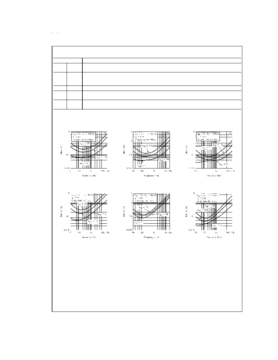
Typical Performance Characteristics
THD+N vs Frequency
DS012607-3
THD+N vs Frequency
DS012607-4
THD+N vs Frequency
DS012607-5
THD+N vs Frequency
DS012607-6
THD+N vs Frequency
DS012607-7
THD+N vs Frequency
DS012607-8
www.national.com
4
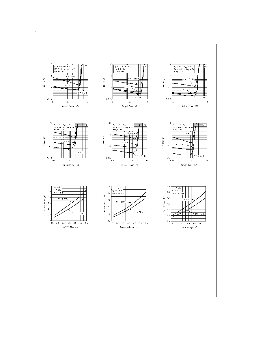
Typical Performance Characteristics
(Continued)
THD+N vs Output Power
DS012607-9
THD+N vs Output Power
DS012607-10
THD+N vs Output Power
DS012607-11
THD+N vs Output Power
DS012607-12
THD+N vs Output Power
DS012607-13
THD+N vs Output Power
DS012607-14
Output Power vs
Supply Voltage
DS012607-15
Output Power vs
Supply Voltage
DS012607-16
Output Power vs
Supply Voltage
DS012607-17
www.national.com
5