 | –≠–ª–µ–∫—Ç—Ä–æ–Ω–Ω—ã–π –∫–æ–º–ø–æ–Ω–µ–Ω—Ç: LM4865M | –°–∫–∞—á–∞—Ç—å:  PDF PDF  ZIP ZIP |
LM4865
750 mW Audio Power Amplifier with DC Volume Control
and Headphone Switch
General Description
The LM4865 is a mono bridged audio power amplifier with
DC volume control, capable of delivering 750 mW of continu-
ous average power into an 8
load with less than 1% THD
from a 5V power supply. Switching between bridged speaker
mode and headphone (single ended) mode is accomplished
via a headphone sense pin. In addition, LM4865 is set into
low current consumption shutdown mode (0.7 µA typical) by
lowering the DC Vol/SD pin to below 0.3V.
Boomer audio power amplifiers are designed specifically to
provide high power audio output, with quality sound, from a
low supply voltage source while requiring the minimal
amount of external components.
Applications
n
GSM phones and accessories, DECT, office phones
n
Hand held radio
n
Other portable audio devices
Key Specifications
n
P
O
at 1.0% THD+N into 8
(SOP): 750 mW (typ)
n
P
O
at 10% THD+N into 8
(SOP): 1W (typ)
n
Shutdown Current: 0.7 µA (typ)
Features
n
DC volume control
n
Headphone amplifier mode
n
"Click and pop" suppression
n
Shutdown control when volume control pin is low
n
Thermal shutdown protection
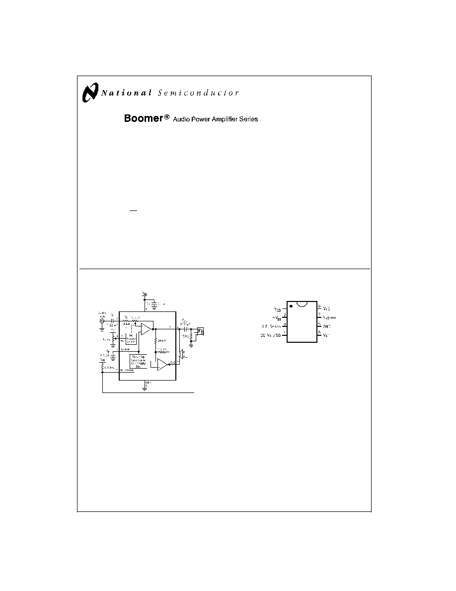
Typical Application
Connection Diagram
BOOMER
TM
is a trademark of National Semiconductor Corporation.
DS101025-1
FIGURE 1. Typical Audio Amplifier
Application Circuit
MSOP, SOP Package
DS101025-2
Top View
Order Number LM4865M, LM4865MM
See NS Package Number M08A, MUA08A
December 1999
LM4865
750
mW
Audio
Power
Amplifier
with
DC
V
olume
Control
and
Headphone
Switch
© 1999 National Semiconductor Corporation
DS101025
www.national.com

Absolute Maximum Ratings
(Note 2)
If Military/Aerospace specified devices are required,
please contact the National Semiconductor Sales Office/
Distributors for availability and specifications.
Supply Voltage
6.0V
Storage Temperature
-65∞C to +150∞C
Input Voltage
-0.3V to V
DD
+0.3V
Power Dissipation (Note 3)
Internally Limited
ESD Susceptibility (Note 4)
2000V
ESD Susceptibility (Note 5)
200V
Junction Temperature
150∞C
Soldering Information
Vapor Phase (60 sec.)
215∞C
Infrared (15 sec.)
220∞C
Thermal Resistance
JC
(SOP)
35∞C/W
JA
(SOP)
150∞C/W
JC
(MSOP)
56∞C/W
JA
(MSOP)
190∞C/W
Operating Ratings
Temperature Range
T
MIN
T
A
T
MAX
-40∞C
T
A
+85∞C
Supply Voltage
2.7V
V
DD
5.5V
See AN-450 "Surface Mounting and their Effects on Product
Reliability" for other methods of soldering surface mount
devices.
Electrical Characteristics
(Notes 1, 2)
he following specifications apply for V
DD
= 5V, unless otherwise specified. Limits apply for T
A
= 25∞C.
Symbol
Parameter
Conditions
LM4865
Units
(Limits)
Typical
(Note 6)
Limit
(Note 7)
V
DD
Supply Voltage
2.7
V (min)
5.5
V (max)
I
DD
Quiescent Power Supply
Current
V
IN
= 0V, I
O
= 0A, HP Sense = 0V
4
7
mA (max)
V
IN
= 0V, I
O
- 0A, HP Sense = 5V
3.5
6
mA (max)
I
SD
Shutdown Current
V
PIN4
0.3V
0.7
µA
V
OS
Output Offset Voltage
V
IN
= 0V
5
50
mV (max)
P
O
Output Power
THD = 1% (max), HP Sense
<
0.8V, f = 1 kHz,
R
L
= 8
750
500
mW
(max)
THD = 10% (max), HP Sense
<
0.8V,
f = 1 kHz, R
L
= 8
1.0
W
THD + N = 1%, HP Sense
>
4V, f = 1 kHz,
R
L
= 32
80
mW
THD = 10%, HP Sense
>
4V, f = 1 kHz,
R
L
= 32
110
mW
THD+N
Total Harmonic Distortion +
Noise
P
O
= 300 mWrms, f = 20 Hz≠20 kHz, R
L
= 8
0.6
%
PSSR
Power Supply Rejection Ratio
V
RIPPLE
= 200 mVrms, R
L
= 8
, C
B
= 1.0 µF,
f = 1 kHz
50
dB
C
RANGE
Attenuator Range-Single Ended
Gain with V
PIN4
4.0V, (80% of V
DD
)
20
18.8
dB (min)
Attenuation with V
PIN4
0.9V, (20% of V
DD
)
-72
-70
dB (min)
V
IH
HP Sense High Input Voltage
4
V (max)
V
IL
HP Sense Low Input Voltage
0.8
V (min)
Note 1: All voltages are measured with respect to the ground pin, unless otherwise specified.
Note 2:
"Absolute Maximum Ratings" indicate limits beyond which damage to the device may occur. "Operating Ratings" indicate conditions for which the device is
functional, but do not guarantee specific performance limits.
"Electrical Characteristics" state DC and AC electrical specifications under particular test conditions which
guarantee specific performance limits. This assumes that the device is within the Operating Ratings. Specifications are not guaranteed for parameters where no limit
is given, however, the typical value is a good indication of device performance.
Note 3: The maximum power dissipation must be derated at elevated temperatures and is dictated by T
JMAX
,
JA
, and the ambient temperature T
A
. The maximum
allowable power dissipation is P
DMAX
= (T
JMAX
- T
A
)/
JA
or the number given in the Absolute Maximum Ratings, whichever is lower. For the LM4865M, T
JMAX
=
150∞C.
Note 4: Human body model, 100 pF discharged through a 1.5 k
resistor.
Note 5: Machine Model, 220 pF≠240 pF discharged through all pins.
Note 6: Typicals are measured at 25∞C and represent the parametric norm.
Note 7: Limits are guaranteed to National's AOQL (Average Outgoing Quality Level).
Note 8: The quiescent power supply current depends on the offset voltage when a practical load is connected to the amplifier.
LM4865
www.national.com
2
External Components Description
(
Figure 1 )
Components
Functional Description
1.
C
i
Input coupling capacitor which blocks the DC voltage at the amplifier's input terminals. It also creates a
highpass filter with the internal R
i
. The designer should note that10kOhm
<
(Ri)
<
110kOhm.Therefore f
c
=
1/(2
R
i
C
i
). Refer to the section, Proper Selection of External Components, for an explanation of how to
determine the value of C
i
.
2.
C
S
Supply bypass capacitor which provides power supply filtering. Refer to the Power Supply Bypassing
section for information concerning proper placement and selection of the supply bypass capacitor.
3.
C
B
Bypass pin capacitor which provides half-supply filtering. Refer to the section, Proper Selection of
External Components, for information concerning proper placement and selection of C
B
.
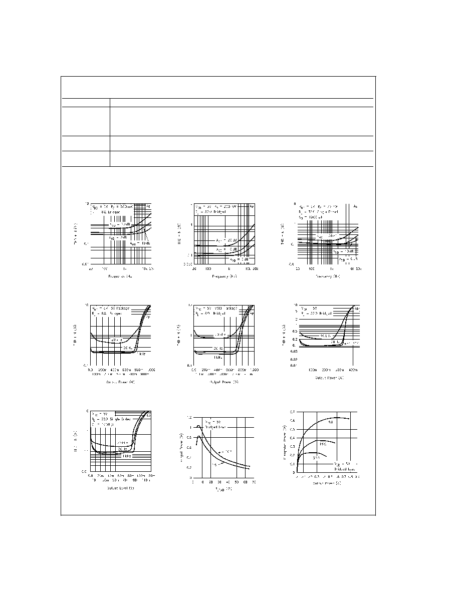
Typical Performance Characteristics
THD+N vs Frequency
DS101025-5
THD+N vs Frequency
DS101025-6
THD+N vs Output Power
DS101025-7
THD+N vs Output Power
DS101025-8
THD+N vs Output Power
DS101025-9
THD+N vs Output Power
DS101025-10
THD+N vs Output Power
DS101025-11
Power Dissipation vs Load
Resistance
DS101025-12
Power Dissipation vs Output Power
DS101025-13
LM4865
www.national.com
3
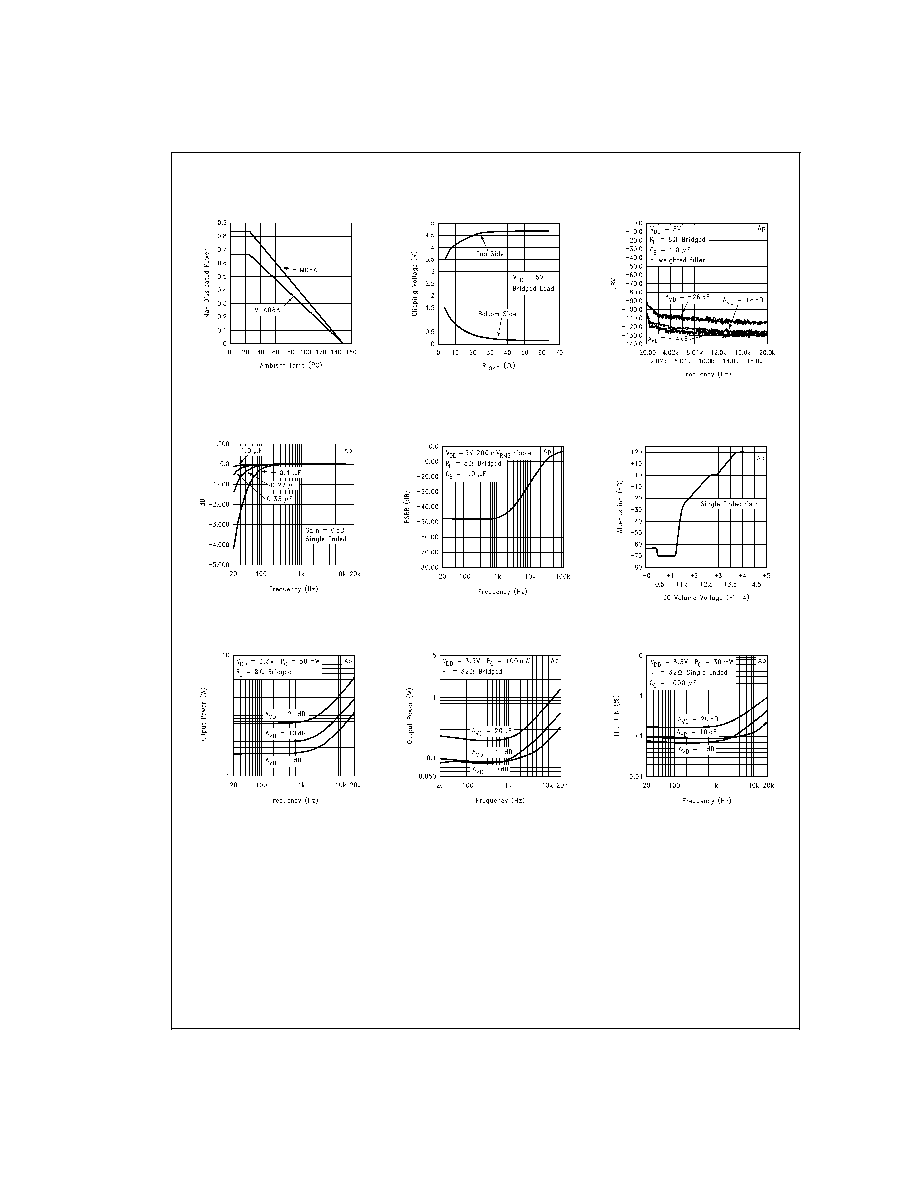
Typical Performance Characteristics
(Continued)
Power Derating Curve
DS101025-14
Clipping Voltage vs RL
DS101025-15
Noise Floor
DS101025-16
Frequency Response vs
Input Capacitor Size
DS101025-17
Power Supply
Rejection Ratio
DS101025-18
Attenuation Level vs
DC-Vol Amplitude
DS101025-19
THD+N vs Frequency
DS101025-20
THD+N vs Frequency
DS101025-21
THD+N vs Frequency
DS101025-22
LM4865
www.national.com
4
Typical Performance Characteristics
(Continued)
Application Information
BRIDGE CONFIGURATION EXPLANATION
As shown in
Figure 1 , the LM4865 has two operational am-
plifiers internally, allowing for a few different amplifier con-
figurations. The first amplifier's gain is DC voltage controlled,
while the second amplifier is internally fixed in a unity-gain,
inverting configuration. The closed-loop gain of the first am-
plifier is set by an external DC voltage (refer to (
Figure 1),
while the second amplifier's gain is fixed by the two internal
20 k
resistors.
Figure 1 shows that the output of amplifier one serves as the
input to amplifier two which results in both amplifiers produc-
ing signals identical in magnitude, but out of phase 180∞.
By driving the load differentially through outputs V
O1
and
V
O2
, an amplifier configuration commonly referred to as
"bridged mode" is established. Bridged mode operation is
different from the classical single-ended amplifier configura-
tion where one side of its load is connected to ground.
A bridge amplifier design has a few distinct advantages over
the single-ended configuration, as it provides differential
drive to the load, thus doubling output swing for a specified
supply voltage. Four times the output power is possible as
compared to a single-ended amplifier under the same condi-
tions. This increase in attainable output assumes that the
amplifier is not current limited or clipped. In order to choose
an amplifier's closed-loop gain without causing excessive
clipping, please refer to the Audio Power Amplifier Design
section.
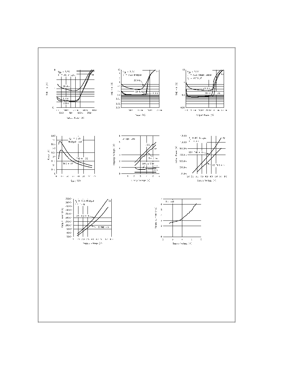
THD+N vs Output Power
DS101025-23
THD+N vs Output Power
DS101025-24
THD+N vs Output Power
DS101025-28
Output Power vs Load Resistance
DS101025-29
Clipping Voltage vs Supply Voltage
DS101025-30
Output Power vs Supply Voltage
DS101025-31
Output Power vs Supply Voltage
DS101025-32
Supply Current vs Supply Voltage
DS101025-33
LM4865
www.national.com
5