LM4865
750 mW Audio Power Amplifier with DC Volume Control
and Headphone Switch
General Description
The LM4865 is a mono bridged audio power amplifier with
DC voltage volume control. The LM4865 is capable of deliv-
ering 750mW of continuous average power into an 8
load
with less than 1% THD when powered by a 5V power supply.
Switching between bridged speaker mode and headphone
(single ended) mode is accomplished using the headphone
sense pin. To conserve power in portable applications, the
LM4865's micropower shutdown mode (I
Q
= 0.7µA, typ) is
activated when less than 300mV is applied to the DC Vol/SD
pin.
Boomer audio power amplifiers are designed specifically to
provide high power audio output while maintaining high fidel-
ity. They require few external components and operate on
low supply voltages.
Applications
n
GSM phones and accessories, DECT, office phones
n
Hand held radio
n
Other portable audio devices
Key Specifications
j
P
O
at 1.0% THD+N into 8
SO, micro SMD
750mW (typ)
j
P
O
at 10% THD+N into 8
SO, micro SMD
1W (typ)
j
Shutdown current
0.7µA(typ)
j
Supply voltage range
2.7V to 5.5V
Features
n
DC voltage volume control
n
Headphone amplifier mode
n
"Click and pop" suppression
n
Shutdown control when volume control pin is low
n
Thermal shutdown protection
Connection Diagrams
micro SMD Package
Small Outline Package (SO)
Mini Small Outline Package (MSOP)
10102536
Top View
Order Number LM4865IBP
See NS Package Number BPA08CFB
10102502
Top View
Order Number LM4865M, LM4865MM
See NS Package Number M08A, MUA08A
BOOMER
TM
is a trademark of National Semiconductor Corporation.
October 2002
LM4865
750
mW
Audio
Power
Amplifier
with
DC
V
olume
Control
and
Headphone
Switch
© 2002 National Semiconductor Corporation
DS101025
www.national.com
Absolute Maximum Ratings
(Note 2)
If Military/Aerospace specified devices are required,
please contact the National Semiconductor Sales Office/
Distributors for availability and specifications.
Supply Voltage
6.0V
Storage Temperature
-65°C to +150°C
Input Voltage
-0.3V to V
DD
+0.3V
Power Dissipation (Note 3)
Internally Limited
ESD Susceptibility (Note 4)
2000V
ESD Susceptibility (Note 5)
200V
Junction Temperature
150°C
Soldering Information
Vapor Phase (60 sec.)
215°C
Infrared (15 sec.)
220°C
Thermal Resistanc
JC
(SOP)
35°C/W
JA
(SOP)
150°C/W
JC
(MSOP)
56°C/W
JA
(MSOP)
190°C/W
JA
(micro SMD)
150°C/W
Operating Ratings
Temperature Range
T
MIN
T
A
T
MAX
-40°C
T
A
+85°C
Supply Voltage
2.7V
V
DD
5.5V
See AN-450 "Surface Mounting and their Effects on Product
Reliability" for other methods of soldering surface mount
devices.
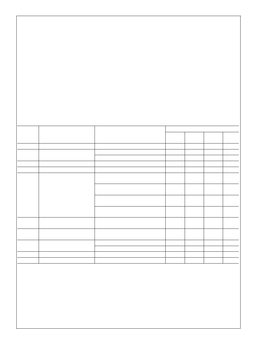
Electrical Characteristics
(Notes 1, 2)
The following specifications apply for V
DD
= 5V, unless otherwise specified. Limits apply for T
A
= 25°C.
Symbol
Parameter
Conditions
LM4865
Min
(Note 7)
Typical
(Note 6)
Max
(Note 7)
Units
V
DD
Supply Voltage
2.7
5.5
V
I
DD
Quiescent Power Supply
Current
V
IN
= 0V, I
O
= 0A, HP Sense = 0V
4
7
mA
V
IN
= 0V, I
O
- 0A, HP Sense = 5V
3.5
6
mA
I
SD
Shutdown Current
V
PIN4
0.3V
0.7
µA
V
OS
Output Offset Voltage
V
IN
= 0V
5
50
mV
P
O
Output Power
THD = 1% (max), HP Sense
<
0.8V,
f = 1kHz, R
L
= 8
500
750
mW
THD = 10% (max), HP Sense
<
0.8V,
f = 1kHz, R
L
= 8
1.0
W
THD + N = 1%, HP Sense
>
4V,
f = 1kHz, R
L
= 32
80
mW
THD = 10%, HP Sense
>
4V,
f = 1kHz, R
L
= 32
110
mW
THD+N
Total Harmonic Distortion +
Noise
P
O
= 300 mWrms, f = 20Hz20kHz,
R
L
= 8
0.6
%
PSRR
Power Supply Rejection Ratio
V
RIPPLE
= 200mVrms, R
L
= 8
, C
B
=
1.0 µF, f = 1kHz
50
dB
Gain
RANGE
Single-Ended Gain Range
Gain with V
PIN4
4.0V, (80% of V
DD
)
18.8
20
dB
Gain with V
PIN4
0.9V, (18% of V
DD
)
-70
-72
dB
V
IH
HP Sense High Input Voltage
4
V
V
IL
HP Sense Low Input Voltage
0.8
V
Note 1: All voltages are measured with respect to the ground pin, unless otherwise specified.
Note 2: "Absolute Maximum Ratings" indicate limits beyond which damage to the device may occur. "Operating Ratings" indicate conditions for which the device
is functional, but do not guarantee specific performance limits. "Electrical Characteristics" state DC and AC electrical specifications under particular test conditions
that guarantee specific performance limits. This assumes that the device operates within the Operating Ratings. Specifications are not guaranteed for parameters
where no limit is given. The typical value, however, is a good indication of device performance.
Note 3: The maximum power dissipation must be derated at elevated temperatures and is dictated by T
JMAX
,
JA
, and the ambient temperature T
A
. The maximum
allowable power dissipation is P
DMAX
= (T
JMAX
- T
A
)/
JA
or the number given in the Absolute Maximum Ratings, whichever is lower. For the LM4865M, T
JMAX
=
150°C.
Note 4: Human body model, 100pF discharged through a 1.5k
resistor.
Note 5: Machine Model, 220pF240pF discharged through all pins.
Note 6: Typicals are measured at 25°C and represent the parametric norm.
Note 7: Limits are guaranteed to National's AOQL (Average Outgoing Quality Level).
Note 8: The quiescent power supply current depends on the offset voltage when a practical load is connected to the amplifier.
LM4865
www.national.com
3
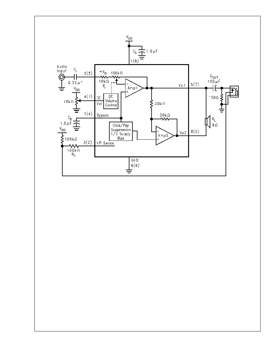
External Components Description
(Figure 1 )
Components
Functional Description
1.
C
i
Input coupling capacitor which blocks the DC voltage at the amplifier's input terminals. It also creates a
highpass filter with the internal R
i
. The designer should note that10kOhm
<
(Ri)
<
110kOhm.Therefore f
c
=
1/(2
R
i
C
i
). Refer to the section, Proper Selection of External Components, for an explanation of how to
determine the value of C
i
.
2.
C
S
Supply bypass capacitor which provides power supply filtering. Refer to the Power Supply Bypassing
section for information concerning proper placement and selection of the supply bypass capacitor.
3.
C
B
Bypass pin capacitor which provides half-supply filtering. Refer to the section, Proper Selection of
External Components, for information concerning proper placement and selection of C
B
.
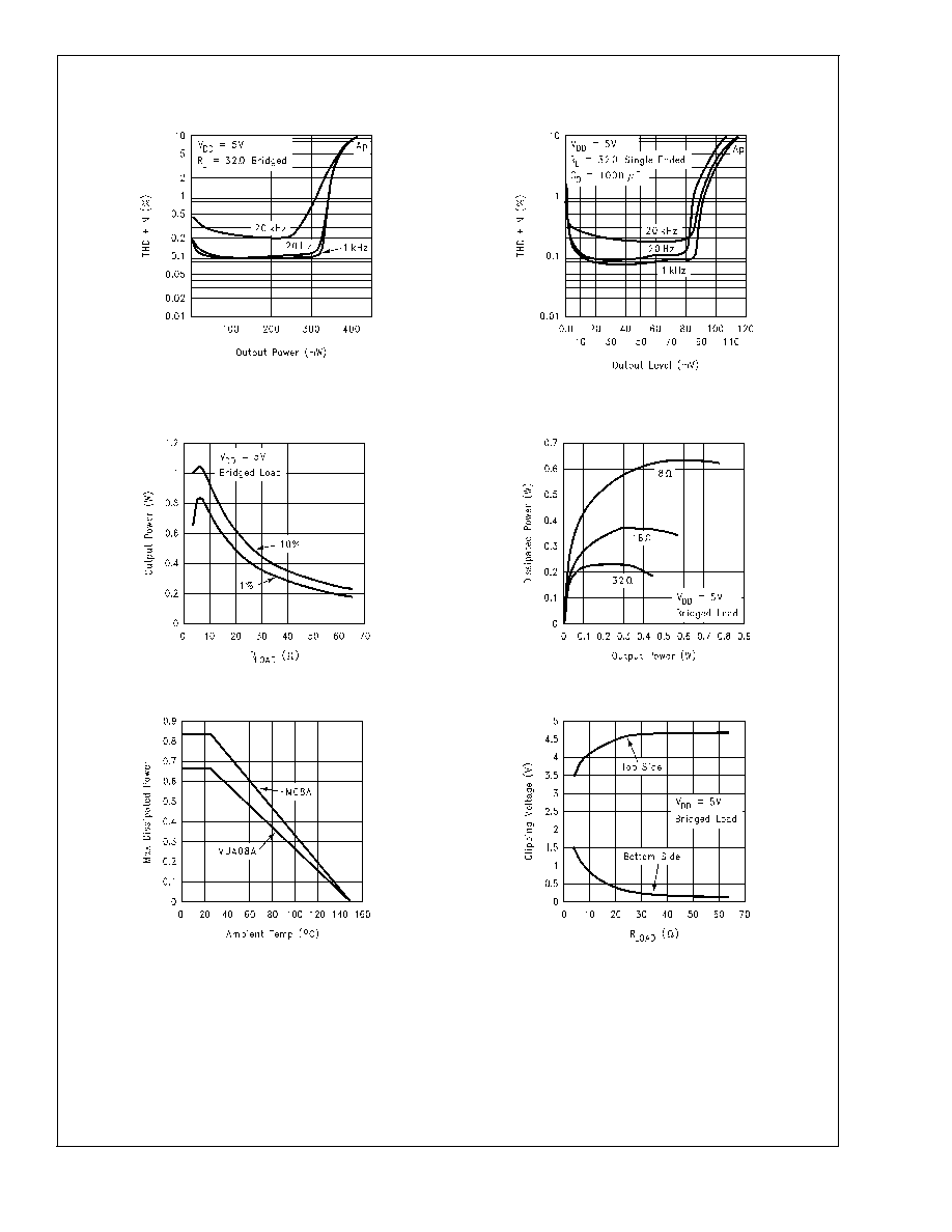
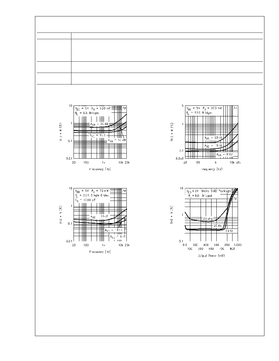
Typical Performance Characteristics
THD+N vs Frequency
THD+N vs Frequency
10102505
10102506
THD+N vs Output Power
THD+N vs Output Power
10102507
10102508
LM4865
www.national.com
4