 | –≠–ª–µ–∫—Ç—Ä–æ–Ω–Ω—ã–π –∫–æ–º–ø–æ–Ω–µ–Ω—Ç: LM4871MM | –°–∫–∞—á–∞—Ç—å:  PDF PDF  ZIP ZIP |
LM4871
3W Audio Power Amplifier with Shutdown Mode
General Description
The LM4871 is a mono bridged audio power amplifier ca-
pable of delivering 3W of continuous average power into a
3
load with less than 10% THD when powered by a 5V
power supply (Note 1). To conserve power in portable appli-
cations, the LM4871's micropower shutdown mode (I
Q
=
0.6µA, typ) is activated when V
DD
is applied to the SHUT-
DOWN pin.
Boomer audio power amplifiers are designed specifically to
provide high power, high fidelity audio output. They require
few external components and operate on low supply volt-
ages from 2.0V to 5.5V. Since the LM4871 does not require
output coupling capacitors, bootstrap capacitors, or snubber
networks, it is ideally suited for low-power portable systems
that require minimum volume and weight.
Additional LM4871 features include thermal shutdown pro-
tection, unity-gain stability, and external gain set.
Note 1: An LM4871LD that has been properly mounted to a circuit board will
deliver 3W into 3
(at 10% THD). The other package options for the LM4871
will deliver 1.5W into 8
(at 10% THD). See the Application Information
sections for further information concerning the LM4871LD, LM4871MM,
LM4871M, and the LM4871N.
Key Specifications
n
PO at 10% THD+N, 1kHz
n
LM4871LD: 3
, 4
loads
3W (typ), 2.5W (typ)
n
All other LM4871 packages: 8
load
1.5W (typ)
n
Shutdown current
0.6µA (typ)
n
Supply voltage range
2.0V to 5.5V
n
THD at 1kHz at 1W continuous average output power
into 8
0.5% (max)
Features
n
No output coupling capacitors, bootstrap capacitors, or
snubber circuits required
n
Unity-gain stable
n
LLP, MSOP, SO, or DIP packaging
n
External gain configuration capability
n
Pin compatible with the LM4861
Applications
n
Portable computers
n
Desktop computers
n
Low voltage audio systems
Typical Application
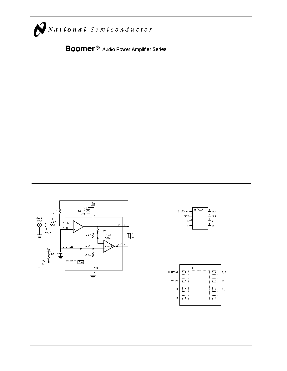
Connection Diagram
Boomer
Æ
is a registered trademark of National Semiconductor Corporation.
DS100008-1
FIGURE 1. Typical Audio Amplifier Application Circuit
MSOP, Small Outline, and DIP Package
DS100008-2
Top View
Order Number LM4871MM, LM4871M, or LM4871N
See NS Package Number MUA08A, M08A, or N08E
LLP Package
DS100008-39
Top View
Order Number LM4871LD
See NS Package Number LDC08A
October 2000
LM4871
3W
Audio
Power
Amplifier
with
Shutdown
Mode
© 2000 National Semiconductor Corporation
DS100008
www.national.com
Absolute Maximum Ratings
(Note 2)
If Military/Aerospace specified devices are required,
please contact the National Semiconductor Sales Office/
Distributors for availability and specifications.
Supply Voltage
6.0V
Supply Temperature
-65∞C to +150∞C
Input Voltage
-0.3V to V
DD
to +0.3V
Power Dissipation (Note 4)
Internally Limited
ESD Susceptibility (Note 5)
5000V
ESD Susceptibility (Note 6)
250V
Junction Temperature
150∞C
Soldering Information
Small Outline Package
Vapor Phase (60 sec.)
215∞C
Infrared (15 sec.)
220∞C
See AN-450
Surface Mounting and their Effects on
Product Reliability
for other methods of
soldering surface mount devices.
JC
(typ) -- M08A
35∞C/W
JA
(typ) -- M08A
140∞C/W
JC
(typ) -- N08E
37∞C/W
JA
(typ) -- N08E
107∞C/W
JC
(typ) -- MUA08A
56∞C/W
JA
(typ) -- MUA08A
210∞C/W
JC
(typ) -- LDC08A
4.3∞C/W
JA
(typ) -- LDC08A
56∞C/W (Note 9)
Operating Ratings
Temperature Range
T
MIN
T
A
T
MAX
-40∞C
T
A
85∞C
Supply Voltage
2.0V
V
DD
5.5V
Electrical Characteristics
(Notes 2, 3)
The following specifications apply for V
DD
= 5V and R
L
= 8
unless otherwise specified. Limits apply for T
A
= 25∞C.
Sym-
bol
Parameter
Conditions
LM4871
Min
(Note 7)
Typical
(Note 8)
Limit
(Note 7)
Units
(Limits)
V
DD
Supply Voltage
2.0
5.5
V
I
DD
Quiescent Power Supply
Current
V
IN
= 0V, I
o
= 0A
6.5
10.0
mA
I
SD
Shutdown Current
V
PIN1
= V
DD
0.6
2
µA
V
OS
Output Offset Voltage
V
IN
= 0V
5.0
50
mV
P
o
Output Power
THD = 1%, f = 1kHz
LM4871LD, R
L
= 3
(Note 10)
LM4871LD, R
L
= 4
(Note 10)
LM4871, R
L
= 8
(Note 10)
2.38
2
1.2
W
THD+N = 10%, f = 1kHz
LM4871LD, R
L
= 3
(Note 10)
LM4871LD, R
L
= 4
(Note 10)
LM4871, R
L
= 8
(Note 10)
3
2.5
1.5
W
THD+N
Total Harmonic
Distortion+Noise
20Hz
f
20kHz, A
VD
= 2
LM4871LD, R
L
= 4
, P
O
= 1.6W
LM4871, R
L
= 8
, P
O
= 1W
0.13
0.25
%
PSRR
Power Supply Rejection
Ratio
V
DD
= 4.9V to 5.1V
60
dB
Note 2:
Absolute Maximum Ratings
indicate limits beyond which damage to the device may occur.
Operating Ratings
indicate conditions for which the device is
functional, but do not guarantee specific performance limits.
Electrical Characteristics
state DC and AC electrical specifications under particular test conditions which
guarantee specific performance limits. This assumes that the device is within the Operating Ratings. Specifications are not guaranteed for parameters where no limit
is given, however, the typical value is a good indication of device performance.
Note 3: All voltages are measured with respect to the ground pin, unless otherwise specified.
Note 4: The maximum power dissipation must be derated at elevated temperatures and is dictated by T
JMAX
,
JA
, and the ambient temperature T
A
. The maximum
allowable power dissipation is P
DMAX
= (T
JMAX
≠T
A
)/
JA
or the number given in Absolute Maximum Ratings, whichever is lower. For the LM4871, T
JMAX
= 150∞C. For
the
JA
's for different packages, please see the Application Information section or the Absolute Maximum Ratings section.
Note 5: Human body model, 100pF discharged through a 1.5k
resistor.
Note 6: Machine Model, 220pF≠240pF discharged through all pins.
Note 7: Typicals are specified at 25∞C and represent the parametric norm.
Note 8: Limits are guaranteed to National's AOQL (Average Outgoing Quality Level).
Note 9: The given
JA
is for an LM4871 packaged in an LDC08A with the Exposed≠DAP soldered to an exposed 1in
2
area of 1oz printed circuit board copper.
Note 10: When driving 3
or 4
loads from a 5V supply, the LM4871LD must be mounted to a circuit board.
LM4871
www.national.com
2
External Components Description
(
Figure 1)
Components
Functional Description
1.
R
i
Inverting input resistance that sets the closed-loop gain in conjunction with R
f
. This resistor also forms a
high pass filter with C
i
at f
C
= 1/(2
R
i
C
i
).
2.
C
i
Input coupling capacitor that blocks the DC voltage at the amplifiers input terminals. Also creates a highpass
filter with R
i
at f
c
= 1/(2
R
i
C
i
). Refer to the section, Proper Selection of External Components, for an
explanation of how to determine the value of C
i
.
3.
R
f
Feedback resistance that sets the closed-loop gain in conjunction with R
i
.
4.
C
S
Supply bypass capacitor that provides power supply filtering. Refer to the Power Supply Bypassing section
for information concerning proper placement and selection of the supply bypass capacitor.
5.
C
B
Bypass pin capacitor that provides half-supply filtering. Refer to the section, Proper Selection of External
Components, for information concerning proper placement and selection of C
B
.
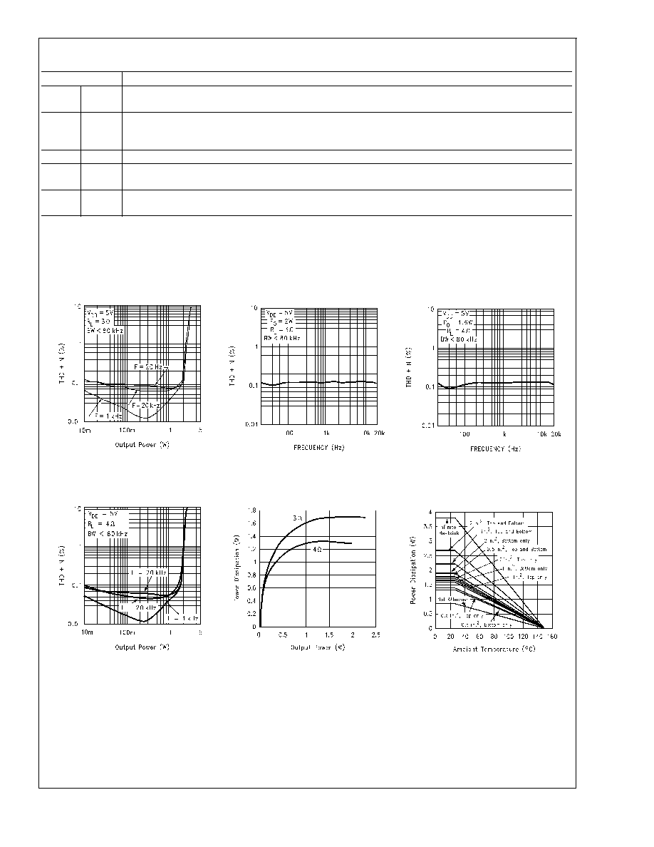
Typical Performance Characteristics
LD Specific Characteristics
Note 11: This curve shows the LM4871LD's thermal dissipation ability at different ambient temperatures given the exposed-DAP of the part is soldered to a plane
of 1oz. Cu with an area given in the label of each curve. This label also designates whether the plane exists on the same (top) layer as the chip, on the bottom layer,
or on both layers. Infinite heatsink and unattached (no heatsink) conditions are also shown.
LM4871LD
THD+N vs Output Power
DS100008-24
LM4871LD
THD+N vs Frequency
DS100008-23
LM4871LD
THD+N vs Frequency
DS100008-25
LM4871LD
THD+N vs Output Power
DS100008-26
LM4871LD
Power Dissipation vs Output Power
DS100008-27
LM4871LD (Note 11)
Power Derating Curve
DS100008-28
LM4871
www.national.com
3
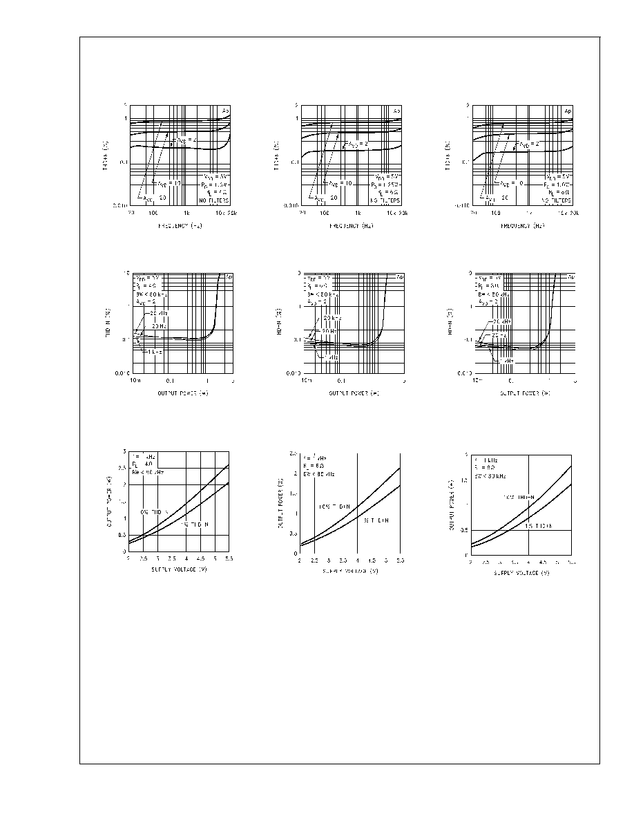
Typical Performance Characteristics
Non-LD Specific Characteristics
THD+N vs Frequency
DS100008-3
THD+N vs Frequency
DS100008-4
THD+N vs Frequency
DS100008-5
THD+N vs Output Power
DS100008-6
THD+N vs Output Power
DS100008-7
THD+N vs Output Power
DS100008-8
Output Power vs
Supply Voltage
DS100008-9
Output Power vs
Supply Voltage
DS100008-10
Output Power vs
Supply Voltage
DS100008-11
LM4871
www.national.com
4
Typical Performance Characteristics
Non-LD Specific Characteristics
(Continued)
Output Power vs
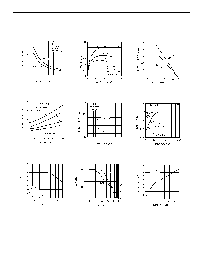
Load Resistance
DS100008-12
Power Dissipation vs
Output Power
DS100008-13
Power Derating Curve
DS100008-14
Clipping Voltage vs
Supply Voltage
DS100008-15
Noise Floor
DS100008-16
Frequency Response vs
Input Capacitor Size
DS100008-17
Power Supply
Rejection Ratio
DS100008-18
Open Loop
Frequency Response
DS100008-19
Supply Current vs
Supply Voltage
DS100008-20
LM4871
www.national.com
5