 | –≠–ª–µ–∫—Ç—Ä–æ–Ω–Ω—ã–π –∫–æ–º–ø–æ–Ω–µ–Ω—Ç: LM4873MTE | –°–∫–∞—á–∞—Ç—å:  PDF PDF  ZIP ZIP |
LM4873
Dual 2.1W Audio Amplifier Plus Stereo Headphone
Function
General Description
The LM4873 is a dual bridge-connected audio power ampli-
fier which, when connected to a 5V supply, will deliver 2.1W
to a 4
load (Note 1) or 2.4W to a 3
load (Note 2)with less
than 1.0% THD+N. In addition, the headphone input pin al-
lows the amplifiers to operate in single-ended mode to drive
stereo headphones. A Mux Control pin toggles between the
two stereo sets of amplifier inputs, allowing for two select-
able amplifier closed-loop responses.
Boomer audio power amplifiers were designed specifically to
provide high quality output power from a surface mount
package while requiring few external components. To sim-
plify audio system design, the LM4873 combines dual bridge
speaker amplifiers and stereo headphone amplifiers on one
chip.
The LM4873 features an externally controlled, low-power
consumption shutdown mode, a stereo headphone amplifier
mode, and thermal shutdown protection. It also utilizes cir-
cuitry to reduce "clicks and pops" during device turn-on.
Note 1: An LM4873MTE-1 which has been properly mounted to the circuit
board will deliver 2.1W into 4
. The other package options for the LM4873
will deliver 1.1W into 8
. See the Application Information section for
LM4873MTE-1 usage information.
Note 2: An LM4873MTE-1 which has been properly mounted to the circuit
board and forced-air cooled will deliver 2.4W into 3
.
Key Specifications
n
P
O
at 1% THD+N
into 3
(LM4873MTE-1)
2.4W(typ)
into 4
(LM4873MTE-1)
2.1W(typ)
into 4
(LM4873MTE)
1.9W(typ)
into 8
(LM4873)
1.1W(typ)
n
Single-ended mode - THD+N
at 75mW into 32
0.5%(max)
n
Shutdown current
0.7µA(typ)
Features
n
Input mux control and two separate inputs per channel
n
Stereo headphone amplifier mode
n
"Click and pop" suppression circuitry
n
Thermal shutdown protection circuitry
n
Exposed-DAP TSSOP and TSSOP packaging available
Applications
n
Multimedia monitors
n
Portable and desktop computers
n
Portable audio systems
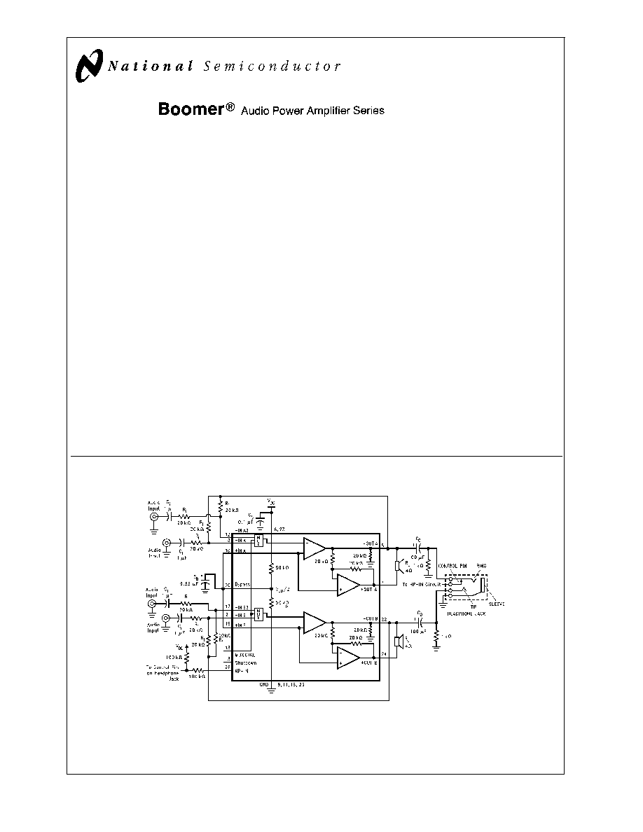
Typical Application
Boomer
Æ
is a registered trademark of National Semiconductor Corporation.
DS100993-31
*
Refer to the section Proper Selection of External Components, for a detailed discussion of C
B
size.
FIGURE 1. Typical Audio Amplifier Application Circuit
April 2000
LM4873
Dual
2.1W
Audio
Amplifier
Plus
Stereo
Headphone
Function
© 2000 National Semiconductor Corporation
DS100993
www.national.com
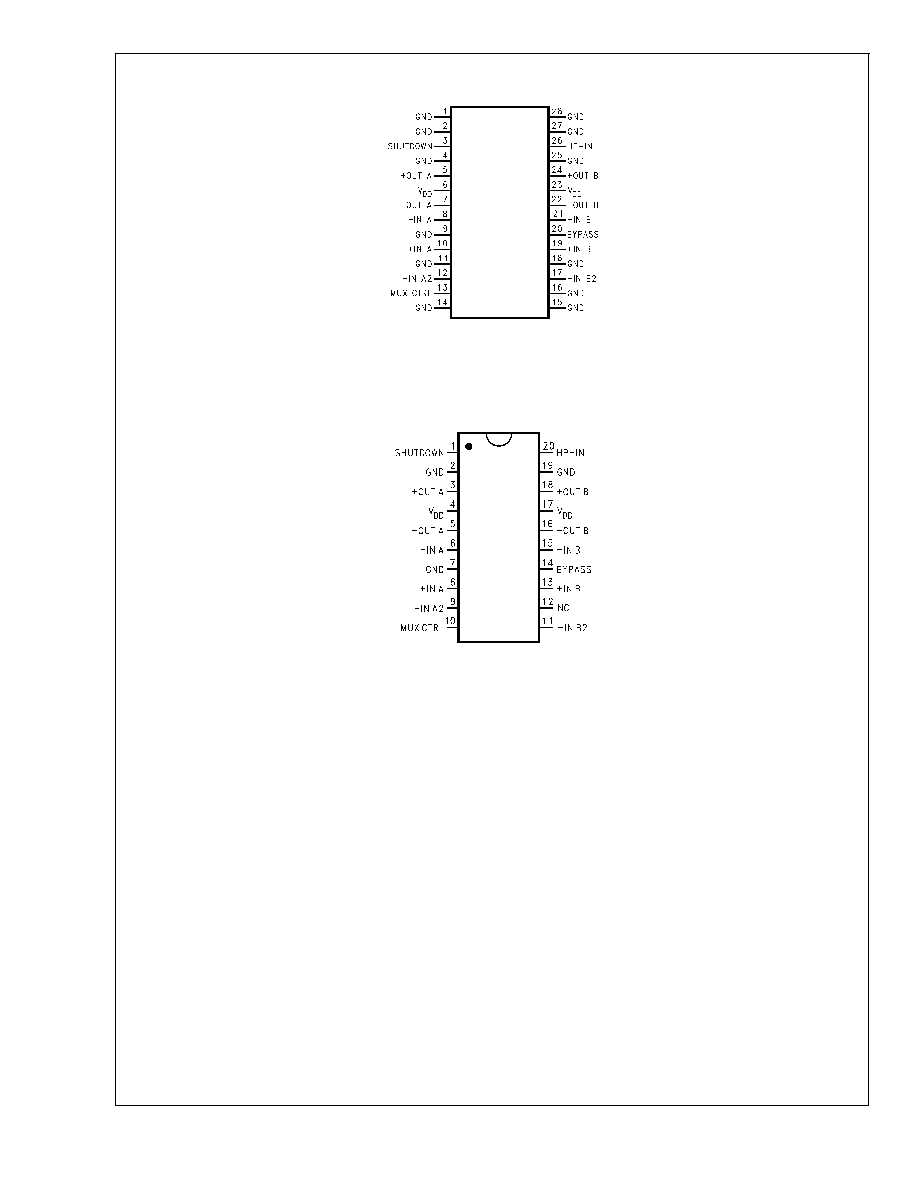
Connection Diagram
Connection Diagram
DS100993-30
Top View
Order Number LM4873MTE-1
See NS Package Number MXA28A for Exposed-DAP TSSOP
DS100993-2
Top View
Order Number LM4873MT, LM4873MTE
See NS Package Number MTC20 for TSSOP
See NS Package Number MXA20A for Exposed-DAP TSSOP
LM4873
www.national.com
2

Absolute Maximum Ratings
(Note 4)
If Military/Aerospace specified devices are required,
please contact the National Semiconductor Sales Office/
Distributors for availability and specifications.
Supply Voltage
6.0V
Storage Temperature
-65∞C to +150∞C
Input Voltage
-0.3V to V
DD
+0.3V
Power Dissipation (Note 14)
Internally limited
ESD Susceptibility (Note 15)
2000V
ESD Susceptibility (Note 16)
200V
Junction Temperature
150∞C
Solder Information
Small Outline Package
Vapor Phase (60 sec.)
215∞C
Infrared (15 sec.)
220∞C
See AN-450 "Surface Mounting and their Effects on
Product Reliablilty" for other methods of soldering surface
mount devices.
Thermal Resistance
JC
(typ) -- M16B
20∞C/W
JA
(typ) -- M16B
80∞C/W
JC
(typ) -- N16A
20∞C/W
JA
(typ) -- N16A
63∞C/W
JC
(typ) -- MTC20
20∞C/W
JA
(typ) -- MTC20
80∞C/W
JC
(typ) -- MXA20A
2∞C/W
JA
(typ) -- MXA20A
41∞C/W (Note 5)
JA
(typ) -- MXA20A
51∞C/W (Note 6)
JA
(typ) -- MXA20A
90∞C/W (Note 7)
JC
(typ) -- MXA28A
2∞C/W
JA
(typ) -- MXA28A
41∞C/W (Note 8)
JA
(typ) -- MXA28A
51∞C/W (Note 9)
JA
(typ) -- MXA28A
90∞C/W (Note 10)
Operating Ratings
Temperature Range
T
MIN
T
A
T
MAX
-40∞C
T
A
85∞C
Supply Voltage
2.0V
V
DD
5.5V
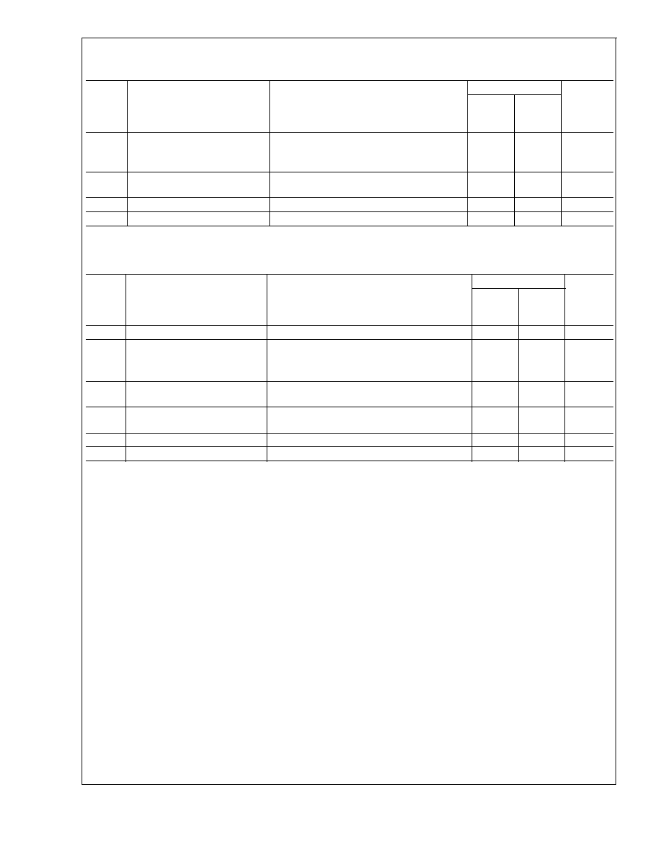
Electrical Characteristics for Entire IC
(Notes 3, 4)
The following specifications apply for V
DD
= 5V unless otherwise noted. Limits apply for T
A
= 25∞C.
Symbol
Parameter
Conditions
LM4873
Units
(Limits)
Typical
Limit
(Note 17)
(Note 18)
V
DD
Supply Voltage
2
V (min)
5.5
V (max)
I
DD
Quiescent Power Supply Current
V
IN
= 0V, I
O
= 0A (Note 19) , HP-IN = 0V
7.5
15
mA (max)
V
IN
= 0V, I
O
= 0A (Note 19) , HP-IN = 4V
5.8
6
mA (min)
I
SD
Shutdown Current
V
PIN1
= V
DD
0.7
2
µA (min)
V
IH
Headphone High Input Voltage
4
V (min)
V
IL
Headphone Low Input Voltage
0.8
V (max)
Electrical Characteristics for Bridged-Mode Operation
(Notes 3, 4)
The following specifications apply for V
DD
= 5V unless otherwise specified. Limits apply for T
A
= 25∞C.
Symbol
Parameter
Conditions
LM4873
Units
(Limits)
Typical
Limit
(Note
17)
(Note
18)
V
OS
Output Offset Voltage
V
IN
= 0V
5
50
mV (max)
P
O
Output Power (Note 13)
THD = 1%, f = 1 kHz
LM4873MTE-1, R
L
= 3
(Note 11)
2.4
W
LM4873MTE, R
L
= 3
(Note 11)
2.2
W
LM4873MTE-1, R
L
= 4
(Note 12)
2.1
W
LM4873MTE, R
L
= 4
(Note 12)
1.9
W
LM4873, R
L
= 8
1.1
1.0
W (min)
THD+N = 10%, f = 1 kHz
LM4873MTE-1, R
L
= 3
(Note 11)
3.0
W
LM4873MTE-1, R
L
= 4
(Note 12)
2.6
LM4873, R
L
= 8
1.5
W
THD+N = 1%, f = 1 kHz, R
L
= 32
0.34
W
LM4873
www.national.com
3
Electrical Characteristics for Bridged-Mode Operation
(Notes 3, 4) (Continued)
The following specifications apply for V
DD
= 5V unless otherwise specified. Limits apply for T
A
= 25∞C.
Symbol
Parameter
Conditions
LM4873
Units
(Limits)
Typical
Limit
(Note
17)
(Note
18)
THD+N
Total Harmonic Distortion+Noise
20 Hz
f
20 kHz, A
VD
= 2
LM4873MTE-1, R
L
= 4
, P
O
= 2W
0.3
LM4873, R
L
= 8
, P
O
= 1W
0.3
%
PSRR
Power Supply Rejection Ratio
V
DD
= 5V, V
RIPPLE
= 200 mV
RMS
, R
L
= 8
,
C
B
= 1.0 µF
67
dB
X
TALK
Channel Separation
f = 1 kHz, C
B
= 1.0 µF
80
dB
SNR
Signal To Noise Ratio
V
DD
= 5V, P
O
= 1.1W, R
L
= 8
97
dB
Electrical Characteristics for Single-Ended Operation
(Notes 3, 4)
The following specifications apply for V
DD
= 5V unless otherwise specified. Limits apply for T
A
= 25∞C.
Symbol
Parameter
Conditions
LM4873
Units
(Limits)
Typical
Limit
(Note
17)
(Note
18)
V
OS
Output Offset Voltage
V
IN
= 0V
5
50
mV (max)
P
O
Output Power
THD = 0.5%, f = 1 kHz, R
L
= 32
85
75
mW (min)
THD+N = 1%, f = 1 kHz, R
L
= 8
340
mW
THD+N = 10%, f = 1 kHz, R
L
= 8
440
mW
THD+N
Total Harmonic Distortion+Noise
A
V
= -1, P
O
= 75 mW, 20 Hz
f
20 kHz,
R
L
= 32
0.2
%
PSRR
Power Supply Rejection Ratio
C
B
= 1.0 µF, V
RIPPLE
= 200 mV
RMS
,
f = 1 kHz
52
dB
X
TALK
Channel Separation
f = 1 kHz, C
B
= 1.0 µF
60
dB
SNR
Signal To Noise Ratio
V
DD
= 5V, P
O
= 340mW, R
L
= 8
94
dB
Note 3: All voltages are measured with respect to the ground pins, 2, 7, and 15, unless otherwise specified.
Note 4: Absolute Maximum Ratings indicate limits beyond which damage to the device may occur. Operating Ratings indicate conditions for which the device is func-
tional, but do not guarantee specific performance limits. Electrical Characteristics state DC and AC electrical specifications under particular test conditions which guar-
antee specific performance limits. This assumes that the device is within the Operating Ratings. Specifications are not guaranteed for parameters where no limit is
given, however, the typical value is a good indication of device performance.
Note 5: The
JA
given is for an MXA20A package whose exposed-DAP is soldered to an exposed 2in
2
piece of 1 ounce printed circuit board copper.
Note 6: The
JA
given is for an MXA20A package whose exposed-DAP is soldered to an exposed 1in
2
piece of 1 ounce printed circuit board copper.
Note 7: The
JA
given is for an MXA20A package whose exposed-DAP is not soldered to any copper.
Note 8: The
JA
given is for an MXA28A package whose exposed-DAP is soldered to an exposed 2in
2
piece of 1 ounce printed circuit board copper.
Note 9: The
JA
given is for an MXA28A package whose exposed-DAP is soldered to an exposed 1in
2
piece of 1 ounce printed circuit board copper.
Note 10: The
JA
given is for an MXA28A package whose exposed-DAP is not soldered to any copper.
Note 11: When driving 3
loads from a 5V supply, the LM4873MTE or LM4873MTE-1 must be mounted to the circuit board and forced-air cooled (450 linear-feet
per minute).
Note 12: When driving 4
loads from a 5V supply, the LM4873MTE or LM4873MTE-1 must be mounted to the circuit board.
Note 13: Output power is measured at the device terminals.
Note 14: The maximum power dissipation must be derated at elevated temperatures and is dictated by T
JMAX
,
JA
, and the ambient temperature T
A
. The maximum
allowable power dissipation is P
DMAX
= (T
JMAX
- T
A
)/
JA
. For the LM4873, T
JMAX
= 150∞C. For the
JA
s for different packages, please see the Application Informa-
tion section or the Absolute Maximum Ratings section.
Note 15: Human body model, 100 pF discharged through a 1.5 k
resistor.
Note 16: Machine model, 220 pF≠240 pF discharged through all pins.
Note 17: Typicals are measured at 25∞C and represent the parametric norm.
Note 18: Limits are guaranteed to National's AOQL (Average Outgoing Quality Level).
Note 19: The quiescent power supply current depends on the offset voltage when a practical load is connected to the amplifier.
LM4873
www.national.com
4
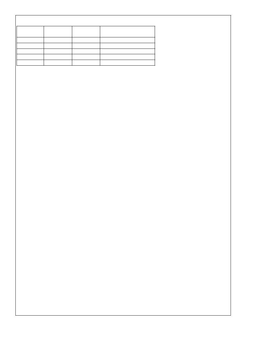
Truth Table for Logic Inputs
SHUTDOWN
HP-IN
INPUT
SELECT
LM4873 MODE (INPUT #)
Low
Low
Low
Bridged (1)
Low
Low
High
Bridged (2)
Low
High
Low
Single-Ended (1)
Low
High
High
Single-Ended (2)
High
X
X
Shutdown
LM4873
www.national.com
5