LM4876
1.1W Audio Power Amplifier with Shutdown Logic Low
General Description
The LM4876 is a bridge-connected audio power amplifier ca-
pable of delivering typically 1.1W of continuous average
power to an 8
load with 0.5% (THD) from a 5V power sup-
ply.
Boomer audio power amplifiers were designed specifically to
provide high quality output power with a minimal amount of
external components. Since the LM4876 does not require
output coupling capacitors, bootstrap capacitors, or snubber
networks, it is optionally suited for low-power portable sys-
tems.
The LM4876 features an externally controlled, low-power
consumption shutdown mode, which is achieved by driving
pin 1 with logic low. Additionally, the LM4876 features an in-
ternal thermal shutdown protection mechanism.
The LM4876 is unity-gain stable and can be configured by
external gain-setting resistors.
Key Specifications
n
THD at 1 kHz at 1W continuous
average output power into 8
0.5% (max)
n
Output power at 10% THD+N
at 1 kHz into 8
1.5W (typ)
n
Shutdown Current
0.01 �A (typ)
Features
n
No output coupling capacitors, bootstrap capacitors, or
snubber circuits are necessary
n
Small Outline packaging
n
Unity-gain stable
n
External gain configuration capability
n
Pin compatible with LM4861 and LM4871
Applications
n
Mobile Phones
n
Portable Computers
n
Desktop Computers
n
Low Voltage Audio Systems
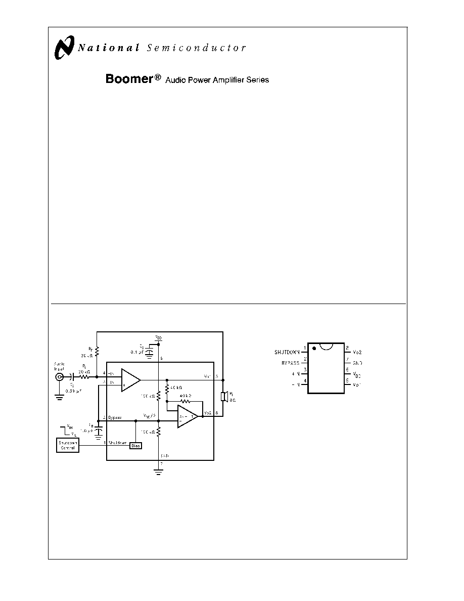
Typical Application
Connection Diagram
Boomer
�
is a registered trademark of National Semiconductor Corporation.
DS101299-1
FIGURE 1. Typical Audio Amplifier Application Circuit
Small Outline Package
DS101299-2
Top View
Order Number LM4876M
See NS Package Number M08A
February 2000
LM4876
1.1W
Audio
Power
Amplifier
with
Shutdown
Logic
Low
� 2000 National Semiconductor Corporation
DS101299
www.national.com
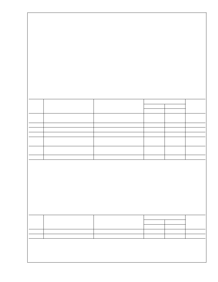
Absolute Maximum Ratings
(Note 2)
If Military/Aerospace specified devices are required,
please contact the National Semiconductor Sales Office/
Distributors for availability and specifications.
Supply Voltage
6.0V
Storage Temperature
-65�C to +150�C
Input Voltage
-0.3V to V
DD
+0.3V
Power Dissipation (Note 3)
Internally Limited
ESD Susceptibility (Note 4)
5000V
ESD Susceptibility (Note 5)
250V
Junction Temperature
150�C
Soldering Information
Small Outline Package
Vapor Phase (60 sec.)
215�C
Infrared (15 sec.)
220�C
See AN-450
Surface Mounting and their Effects on
Product Reliability
for other methods of
soldering surface mount devices.
JC
(typ) -- M08A
35�C/W
JA
(typ) -- M08A
140�C/W
Operating Ratings
Temperature Range
T
MIN
T
A
T
MAX
-40�C
T
A
85�C
Supply Voltage
2.0V
V
DD
5.5V
Electrical Characteristics
(Notes 1, 2)
The following specifications apply for V
DD
= 5V unless otherwise specified. Limits apply for T
A
= 25�C.
Symbol
Parameter
Conditions
LM4876
Units
(Limits)
Typical
Limit
(Note 6)
(Note 7)
V
DD
Supply Voltage
2.0
V (min)
5.5
V (max)
I
DD
Quiescent Power Supply Current
V
IN
= 0V, I
o
= 0A
6.5
10.0
mA (max)
I
SD
Shutdown Current
V
PIN1
= 0V
0.01
2
�A (max)
V
OS
Output Offset Voltage
V
IN
= 0V
5
50
mV (max)
P
o
Output Power
THD = 0.5% (max); f = 1 kHz
1.10
1.0
W (min)
THD+N = 10%; f = 1 kHz
1.5
W
THD+N
Total Harmonic Distortion+Noise
P
o
= 1 Wrms; A
VD
= 2; 20 Hz
f
20 kHz
0.25
%
PSRR
Power Supply Rejection Ratio
V
DD
= 4.9V to 5.1V
65
dB
Note 1: All voltages are measured with respect to the ground pin, unless otherwise specified.
Note 2:
Absolute Maximum Ratings
indicate limits beyond which damage to the device may occur.
Operating Ratings
indicate conditions for which the device is func-
tional, but do not guarantee specific performance limits.
Electrical Characteristics
state DC and AC electrical specifications under particular test conditions which guar-
antee specific performance limits. This assumes that the device is within the Operating Ratings. Specifications are not guaranteed for parameters where no limit is
given, however, the typical value is a good indication of device performance.
Note 3: The maximum power dissipation must be derated at elevated temperatures and is dictated by T
JMAX
,
JA
, and the ambient temperature T
A
. The maximum
allowable power dissipation is P
DMAX
= (T
JMAX
�T
A
)/
JA
or the number given in Absolute Maximum Ratings, whichever is lower. For the LM4876, T
JMAX
= 150�C. The
typical junction-to-ambient thermal resistance is 140�C/W for package number M08A.
Note 4: Human body model, 100 pF discharged through a 1.5 k
resistor.
Note 5: Machine Model, 220 pF�240 pF discharged through all pins.
Note 6: Typicals are measured at 25�C and represent the parametric norm.
Note 7: Limits are guaranteed to National's AOQL (Average Outgoing Quality Level).
Electrical Characteristics V
DD
= 5/3.3/2.6V
Symbol
Parameter
Conditions
LM4876
Units
(Limits)
Typical
Limit
(Note 6)
(Note 7)
V
IH
Shutdown Input Voltage High
1.2
V(min)
V
IL
Shutdown Input Voltage Low
0.4
V(max)
LM4876
www.national.com
2
External Components Description
(
Figure 1)
Components
Functional Description
1.
R
i
Inverting input resistance which sets the closed-loop gain in conjunction with R
f
. This resistor also forms a
high pass filter with C
i
at f
C
= 1/(2
R
i
C
i
).
2.
C
i
Input coupling capacitor which blocks the DC voltage at the amplifiers input terminals. Also creates a
highpass filter with R
i
at f
c
= 1/(2
R
i
C
i
). Refer to the section, Proper Selection of External Components,
for an explanation of how to determine the value of C
i
.
3.
R
f
Feedback resistance which sets the closed-loop gain in conjunction with R
i
.
4.
C
S
Supply bypass capacitor which provides power supply filtering. Refer to the Power Supply Bypassing
section for information concerning proper placement and selection of the supply bypass capacitor.
5.
C
B
Bypass pin capacitor which provides half-supply filtering. Refer to the section, Proper Selection of External
Components, for information concerning proper placement and selection of C
B
.
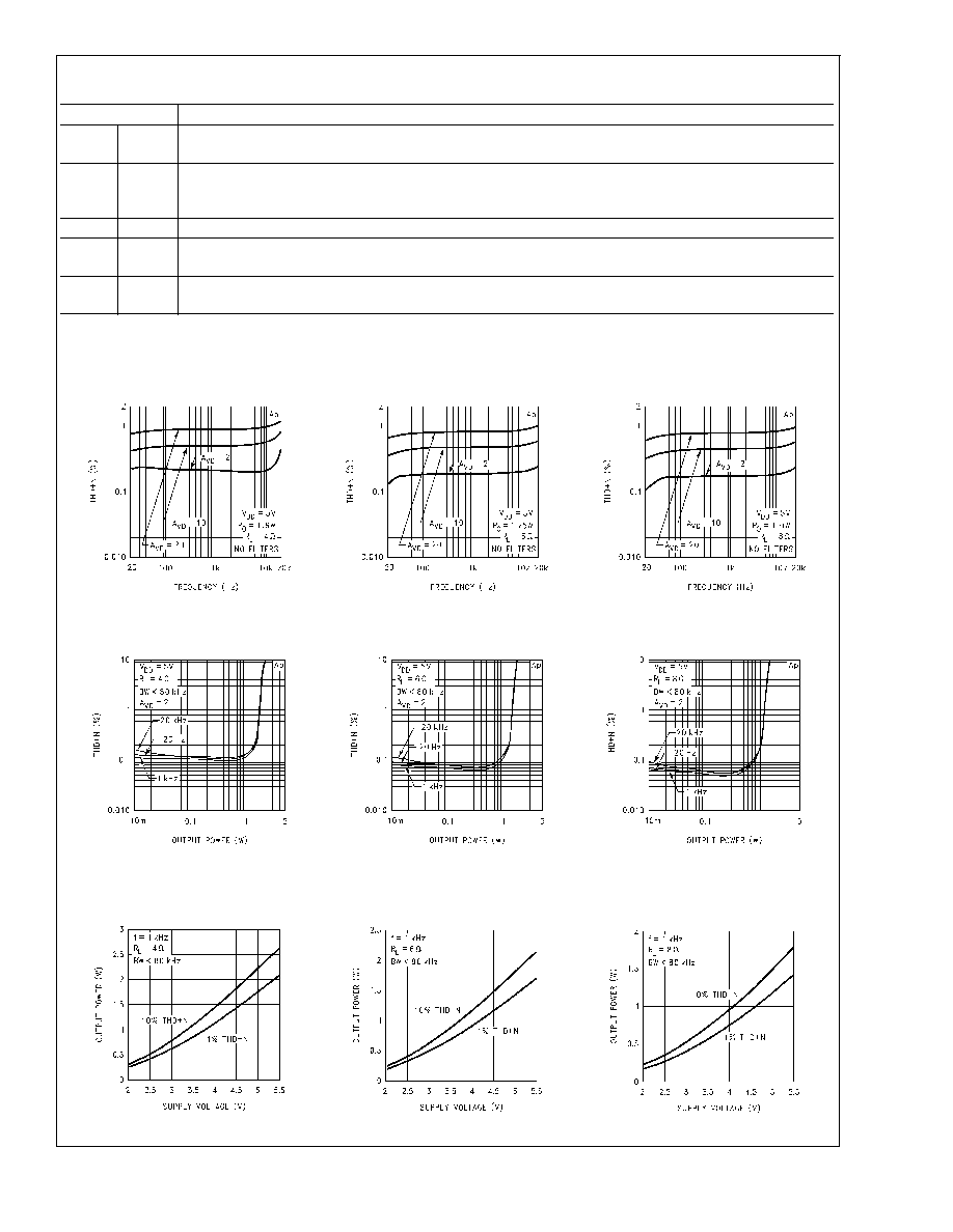
Typical Performance Characteristics
THD+N vs Frequency
DS101299-3
THD+N vs Frequency
DS101299-4
THD+N vs Frequency
DS101299-5
THD+N vs Output Power
DS101299-6
THD+N vs Output Power
DS101299-7
THD+N vs Output Power
DS101299-8
Output Power vs
Supply Voltage
DS101299-9
Output Power vs
Supply Voltage
DS101299-10
Output Power vs
Supply Voltage
DS101299-11
LM4876
www.national.com
3
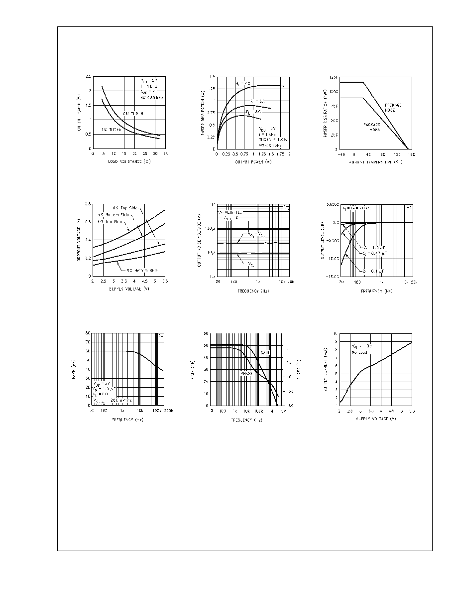
Typical Performance Characteristics
(Continued)
Output Power vs
Load Resistance
DS101299-12
Power Dissipation vs
Output Power
DS101299-13
Power Derating Curve
DS101299-14
Clipping Voltage vs
Supply Voltage
DS101299-15
Noise Floor
DS101299-16
Frequency Response vs
Input Capacitor Size
DS101299-17
Power Supply
Rejection Ratio
DS101299-18
Open Loop
Frequency Response
DS101299-19
Supply Current vs
Supply Voltage
DS101299-20
LM4876
www.national.com
4
Typical Performance Characteristics
(Continued)
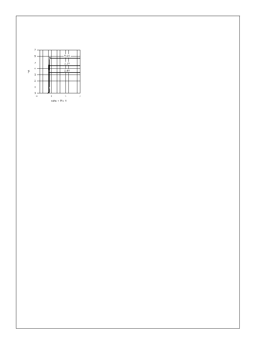
Supply Current vs
Shutdown Voltage
LM4876
@
VDD = 5/3.3/2.6Vdc
DS101299-23
LM4876
www.national.com
5