LM4876
1.1W Audio Power Amplifier with Logic Low Shutdown
General Description
The LM4876 is a single 5V supply bridge-connected audio
power amplifier capable of delivering 1.1W (typ) of continu-
ous average power to an 8
load with 0.5% THD+N.
Like other audio amplifiers in the Boomer series, the LM4876
is designed specifically to provide high quality output power
with a minimal amount of external components. The LM4876
does not require output coupling capacitors, bootstrap ca-
pacitors, or snubber networks. It is perfectly suited for low-
power portable systems.
The LM4876 features an active low externally controlled,
micro-power shutdown mode. Additionally, the LM4876 fea-
tures an internal thermal shutdown protection mechanism.
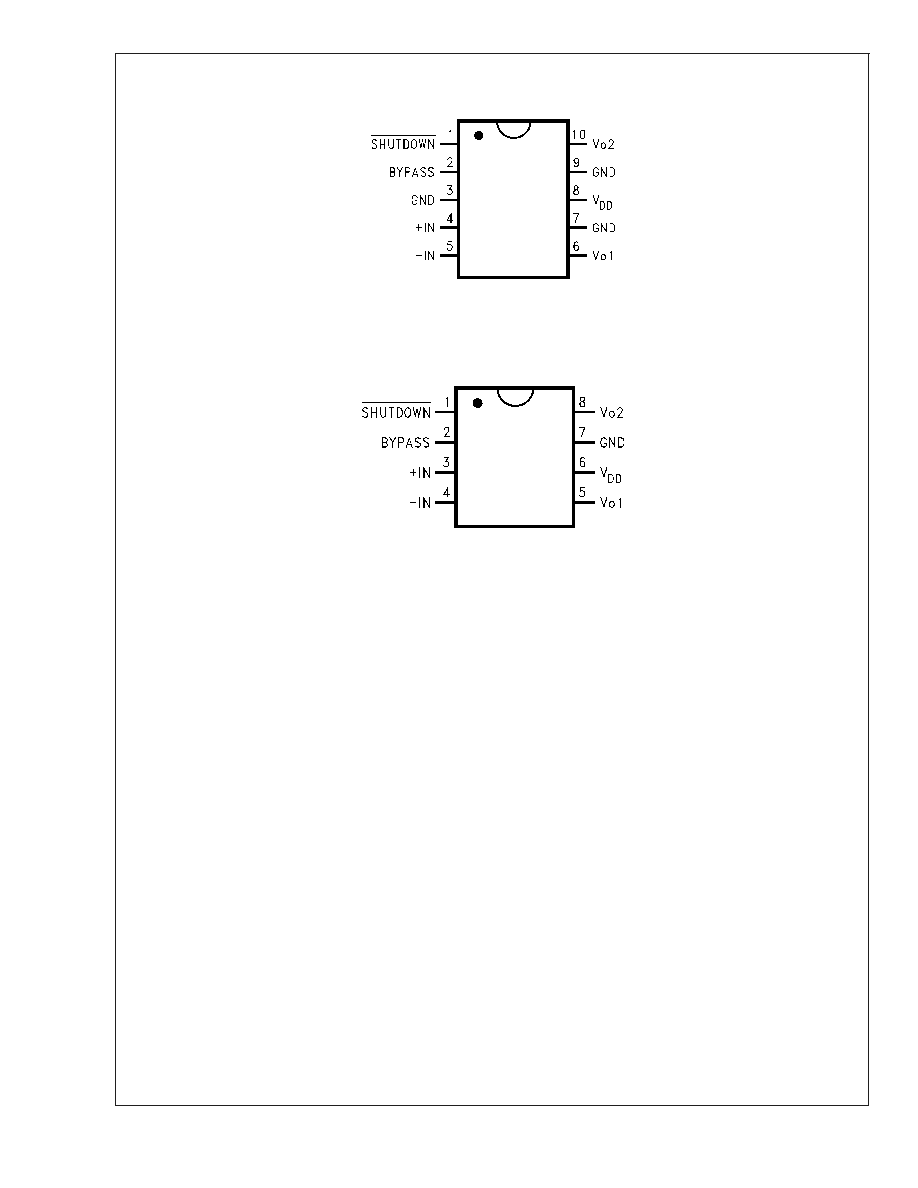
For PCB space efficiency, the LM4876 is available in MSOP
and SO surface mount packages.
The unity-gain stable LM4876's closed loop gain is set using
external resistors.
Key Specifications
j
THD+N at 1kHz for 1W continuous
average output power into 8
0.5% (max)
j
Output power at 1kHz into 8
with 10% THD+N
1.5W (typ)
j
Shutdown current
0.01�A (typ)
j
Supply voltage range
2.0V to 5.5V
Features
n
Does not require output coupling capacitors, bootstrap
capacitors, or snubber circuits
n
10-pin MSOP and 8-pin SO packages
n
Unity-gain stable
n
External gain set
Applications
n
Mobile Phones
n
Portable Computers
n
Desktop Computers
n
Low-Voltage Audio Systems
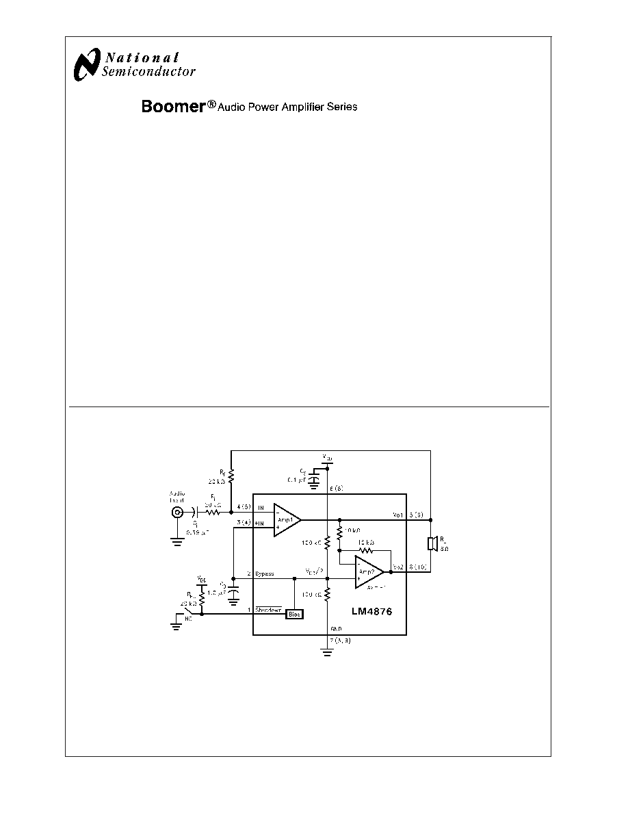
Typical Application
Boomer
�
is a registered trademark of National Semiconductor Corporation.
10129901
FIGURE 1. Typical LM4876 Audio Amplifier Application Circuit.
Numbers in ( ) are specific to the 10-pin MSOP package
March 2003
LM4876
1.1W
Audio
Power
Amplifier
with
Logic
Low
Shutdown
� 2003 National Semiconductor Corporation
DS101299
www.national.com
Absolute Maximum Ratings
(Note 2)
If Military/Aerospace specified devices are required,
please contact the National Semiconductor Sales Office/
Distributors for availability and specifications.
Supply Voltage
6.0V
Storage Temperature
-65�C to +150�C
Input Voltage
-0.3V to V
DD
+0.3V
Power Dissipation (Note 3)
Internally Limited
ESD Susceptibility (Note 4)
2500V
ESD Susceptibility (Note 5)
250V
Junction Temperature
150�C
Soldering Information
Small Outline Package
Vapor Phase (60 sec.)
215�C
Infrared (15 sec.)
220�C
See AN-450 "Surface Mounting and their Effects on
Product Reliability" for other methods of
soldering surface mount devices.
JC
(typ) -- MUB10A
56�C/W
JA
(typ) -- MUB10A
210�C/W
JC
(typ) -- M08A
35�C/W
JA
(typ) -- M08A
140�C/W
Operating Ratings
Temperature Range
T
MIN
T
A
T
MAX
-40�C
T
A
85�C
Supply Voltage
2.0V
V
DD
5.5V
Electrical Characteristics
(Notes 1, 2)
The following specifications apply for V
DD
= 5V unless otherwise specified. Limits apply for T
A
= 25�C.
Symbol
Parameter
Conditions
LM4876
Units
(Limits)
Typical
Limit
(Note 6)
(Note 7)
V
DD
Supply Voltage
2.0
V (min)
5.5
V (max)
I
DD
Quiescent Power Supply Current
V
IN
= 0V, I
o
= 0A
6.5
10.0
mA (max)
I
SD
Shutdown Current
V
PIN1
= 0V
0.01
2
�A (max)
V
OS
Output Offset Voltage
V
IN
= 0V
5
50
mV (max)
P
o
Output Power
THD = 0.5% (max); f = 1 kHz;
R
L
= 8
1.10
1.0
W (min)
THD+N = 10%; f = 1 kHz;
R
L
= 8
1.5
W
THD+N
Total Harmonic Distortion+Noise
P
o
= 1 Wrms; A
VD
= 2; 20 Hz
f
20 kHz; R
L
= 8
0.25
%
PSRR
Power Supply Rejection Ratio
V
DD
= 4.9V to 5.1V
65
dB
Note 1: All voltages are measured with respect to the ground pin, unless otherwise specified.
Note 2: Absolute Maximum Ratings indicate limits beyond which damage to the device may occur. Operating Ratings indicate conditions for which the device is
functional, but do not guarantee specific performance limits. Electrical Characteristics state DC and AC electrical specifications under particular test conditions that
guarantee specific performance limits. This assumes that the device operates within the Operating Ratings. Specifications are not guaranteed for parameters where
no limit is given. The typical value, however, is a good indication of device performance.
Note 3: The maximum power dissipation must be derated at elevated temperatures and is dictated by T
JMAX
,
JA
, and the ambient temperature T
A
. The maximum
allowable power dissipation is P
DMAX
= (T
JMAX
�T
A
)/
JA
or the number given in Absolute Maximum Ratings, whichever is lower. For the LM4876, T
JMAX
= 150�C.
The typical junction-to-ambient thermal resistance is 140�C/W for the M08A package and 210�C/W for the MUB10A package.
Note 4: Human body model, 100 pF discharged through a 1.5 k
resistor.
Note 5: Machine Model, 220 pF�240 pF discharged through all pins.
Note 6: Typicals are measured at 25�C and represent the parametric norm.
Note 7: Limits are guaranteed to National's AOQL (Average Outgoing Quality Level).
Electrical Characteristics V
DD
= 5/3.3/2.6V
Symbol
Parameter
Conditions
LM4876
Units
(Limits)
Typical
Limit
(Note 6)
(Note 7)
V
IH
Shutdown Input Voltage High
1.2
V(min)
V
IL
Shutdown Input Voltage Low
0.4
V(max)
LM4876
www.national.com
3
External Components Description
(Figure 1)
Components
Functional Description
1.
R
i
Inverting input resistance which sets the closed-loop gain in conjunction with R
f
. This resistor also forms a
high pass filter with C
i
at f
C
= 1/(2
R
i
C
i
).
2.
C
i
Input coupling capacitor which blocks the DC voltage at the amplifiers input terminals. Also creates a
highpass filter with R
i
at f
C
= 1/(2
R
i
C
i
). Refer to the section, Proper Selection of External Components,
for an explanation of how to determine the value of C
i
.
3.
R
f
Feedback resistance which sets the closed-loop gain in conjunction with R
i
.
4.
C
S
Supply bypass capacitor which provides power supply filtering. Refer to the Power Supply Bypassing
section for information concerning proper placement and selection of the supply bypass capacitor.
5.
C
B
Bypass pin capacitor which provides half-supply filtering. Refer to the section, Proper Selection of External
Components, for information concerning proper placement and selection of C
B
.
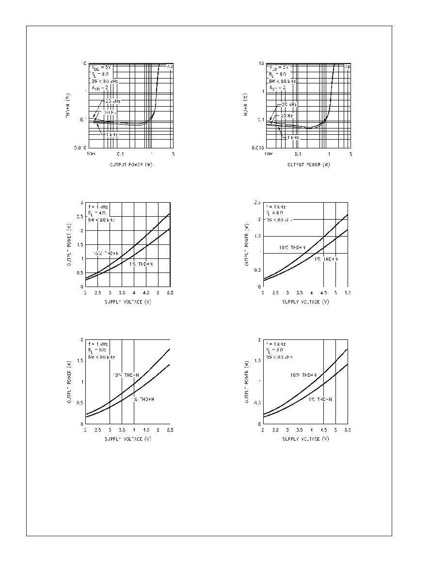
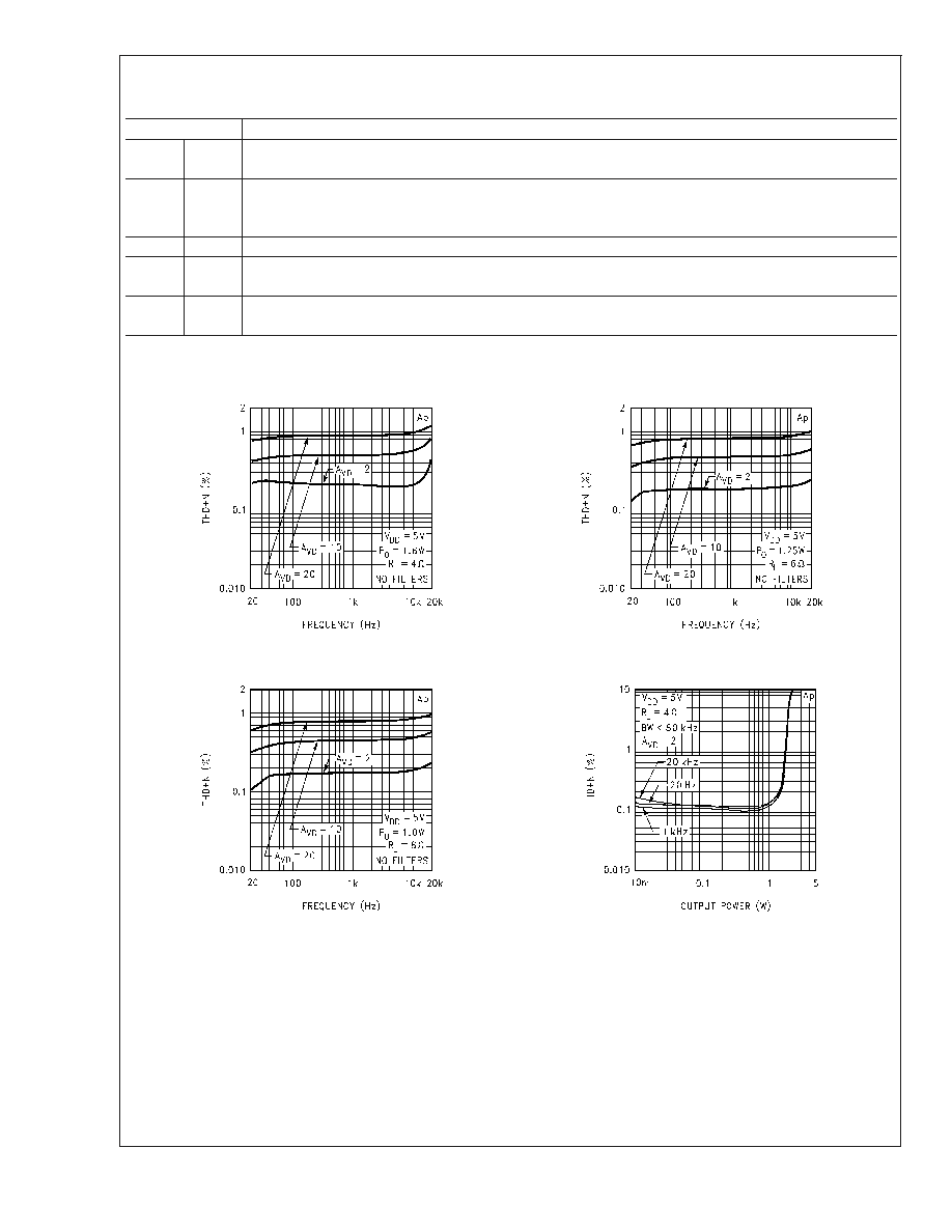
Typical Performance Characteristics
THD+N vs Frequency
THD+N vs Frequency
10129903
10129904
THD+N vs Frequency
THD+N vs Output Power
10129905
10129906
LM4876
www.national.com
4