 | –≠–ª–µ–∫—Ç—Ä–æ–Ω–Ω—ã–π –∫–æ–º–ø–æ–Ω–µ–Ω—Ç: LM4880 | –°–∫–∞—á–∞—Ç—å:  PDF PDF  ZIP ZIP |
LM4880
Dual 250 mW Audio Power Amplifier with Shutdown
Mode
General Description
The LM4880 is a dual audio power amplifier capable of deliv-
ering typically 250 mW per channel of continuous average
power to an 8
load with 0.1% (THD) using a 5V power sup-
ply.
Boomer audio power amplifiers were designed specifically to
provide high quality output power with a minimal amount of
external components using surface mount packaging.
Since the LM4880 does not require bootstrap capacitors or
snubber networks, it is optimally suited for low-power por-
table systems.
The LM4880 features an externally controlled, low-power
consumption shutdown mode, as well as an internal thermal
shutdown protection mechanism.
The unity-gain stable LM4880 can be configured by external
gain-setting resistors.
Key Specifications
n
THD at 1 kHz at 200 mW continuous average output
power into 8
:
0.1% (max)
n
THD at 1 kHz at 85 mW continuous average output
power into 32
:
0.1% (typ)
n
Output power at 10% THD + N at 1 kHz into 8
:
325 mW (typ)
n
Shutdown Current:
0.7 µA (typ)
Features
n
No bootstrap capacitors or snubber circuits are
necessary
n
Small Outline (SO) and DIP packaging
n
Unity-gain stable
n
External gain configuration capability
Applications
n
Headphone Amplifier
n
Personal Computers
n
CD-ROM Players
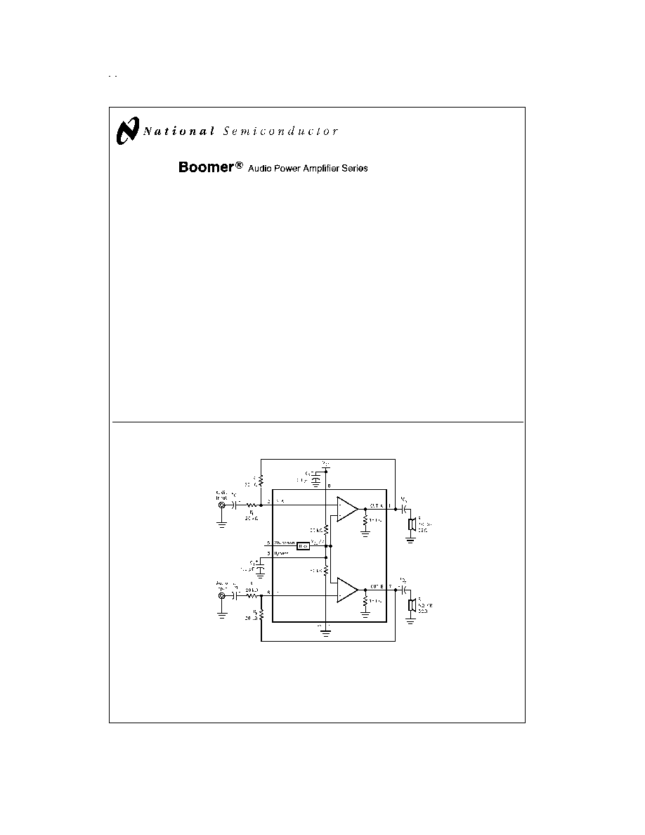
Typical Application
Boomer
Æ
is a registered trademark of National Semiconductor Corporation.
DS012343-1
*
Refer to the Application Information section for information concerning proper selection of the input and output coupling capacitors.
FIGURE 1. Typical Audio Amplifier Application Circuit
November 1995
LM4880
Boomer
Audio
Power
Amplifier
Series
Dual
250
mW
Audio
Power
Amplifier
with
Shutdown
Mode
© 1999 National Semiconductor Corporation
DS012343
www.national.com
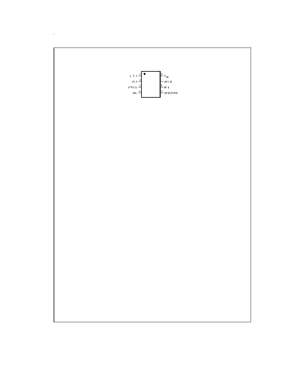
Connection Diagram
Small Outline and
DIP Packages
DS012343-2
Top View
Order Number LM4880M or LM4880N
See NS Package Number M08A for SO
or NS Package Number N08E for DIP
www.national.com
2
Absolute Maximum Ratings
(Note 2)
If Military/Aerospace specified devices are required,
please contact the National Semiconductor Sales Office/
Distributors for availability and specifications.
Supply Voltage
6.0V
Storage Temperature
-65∞C to +150∞C
Input Voltage
-0.3V to V
DD
+ 0.3V
Power Dissipation (Note 3)
Internally limited
ESD Susceptibility (Note 4)
3500V
ESD Susceptibility (Note 5)
250V
Junction Temperature
150∞C
Soldering Information
Small Outline Package
Vapor Phase (60 sec.)
Infrared (15 sec.)
215∞C
220∞C
See AN-450 "Surface Mounting and their Effects on
Product Reliability" for other methods of soldering surface
mount devices.
Thermal Resistance
JC
(DIP)
37∞C/W
JA
(DIP)
107∞C/W
JC
(SO)
35∞C/W
JA
(SO)
170∞C/W
Operating Ratings
Temperature Range
T
MIN
T
A
T
MAX
-40∞C
T
A
+85∞C
Supply Voltage
2.7V
V
DD
5.5V
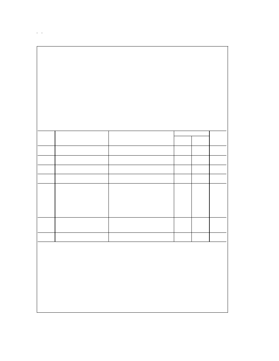
Electrical Characteristics
(Notes 1, 2)
The following specifications apply for V
DD
= 5V unless otherwise specified. Limits apply for T
A
= 25∞C.
Symbol
Parameter
Conditions
LM4880
Units
(Limits)
Typical
Limit
(Note 6)
(Note 7)
V
DD
Supply Voltage
2.7
V (min)
5.5
V (max)
I
DD
Quiescent Power Supply Current
V
IN
=0V, I
O
=0A
3.6
6.0
mA
(max)
I
SD
Shutdown Current
V
PIN5
=V
DD
0.7
5
µA
(max)
V
OS
Output Offset Voltage
V
IN
=0V
5
50
mV
(max)
P
O
Output Power
THD=0.1% (max); f=1 kHz;
R
L
=8
250
200
mW
(min)
R
L
=32
85
mW
THD+N=10%; f=1 kHz
R
L
=8
325
mW
R
L
=32
110
mW
THD+N
Total Harmonic Distortion+Noise
R
L
=8
, P
O
=200 mW;
0.03
%
R
L
=32
, P
O
=75 mW;
0.02
%
f=1 kHz
PSRR
Power Supply Rejection Ratio
C
B
= 1.0 µF,
V
RIPPLE
=200 mVrms, f = 100 Hz
50
dB
Note 1: All voltages are measured with respect to the ground pin, unless otherwise specified.
Note 2: Absolute Maximum Ratings indicate limits beyond which damage may occur. Operating Ratings indicate conditions for which the device is functional, but do
not guarantee specific performance limits. Electrical Characteristics state DC and AC electrical specifications under particular test conditions which guarantee specific
performance limits. This assumes that the device is within the Operating Ratings. Specifications are not guaranteed for parameters where no limit is given, however,
the typical value is a good indication of device performance.
Note 3: The maximum power dissipation must be derated at elevated temperatures and is dictated by T
JMAX
,
JA
, and the ambient temperature T
A
. The maximum
allowable power dissipation is P
DMAX
= (T
JMAX
- T
A
)/
JA
or the number given in the Absolute Maximum Ratings, whichever is lower. For the LM4880, T
JMAX
= 150∞C,
and the typical junction-to-ambient thermal resistance is 170∞C/W for package M08A and 107∞C/W for package N08E.
Note 4: Human body model, 100 pF discharged through a 1.5 k
resistor.
Note 5: Machine model, 220 pF≠240 pF discharged through all pins.
Note 6: Typicals are measured at 25∞C and represent the parametric norm.
Note 7: Limits are guaranteed to National's AOQL (Average Outgoing Quality Level).
www.national.com
3

Automatic Shutdown Circuit
Automatic Switching Circuit
External Components Description
(
Figure 1)
Components
Functional Description
1.
R
i
Inverting input resistance which sets the closed-loop gain in conjunction with R
F
. This resistor
also forms a high pass filter with C
i
at f
c
= 1/(2
R
i
C
i
).
2.
C
i
Input coupling capacitor which blocks the DC voltage at the amplifier's input terminals. Also
creates a high pass filter with R
i
at f
c
= 1/(2
R
i
C
i
). Refer to the section, Proper Selection of
External Components, for an explanation of how to determine the value of C
i
.
3.
R
F
Feedback resistance which sets closed-loop gain in conjunction with R
i
.
DS012343-3
FIGURE 2. Automatic Shutdown Circuit
DS012343-4
FIGURE 3. Automatic Switching Circuit
www.national.com
4
External Components Description
(
Figure 1) (Continued)
Components
Functional Description
4.
C
S
Supply bypass capacitor which provides power supply filtering. Refer to the Application
Information section for proper placement and selection of the supply bypass capacitor.
5.
C
B
Bypass pin capacitor which provides half-supply filtering. Refer to the section, Proper
Selection of External Components, for information concerning proper placement and
selection of C
B
.
6.
C
o
Output coupling capacitor which blocks the DC voltage at the amplifier's output. Forms a high
pass filter with R
L
at f
o
= 1/(2
R
L
C
o
).
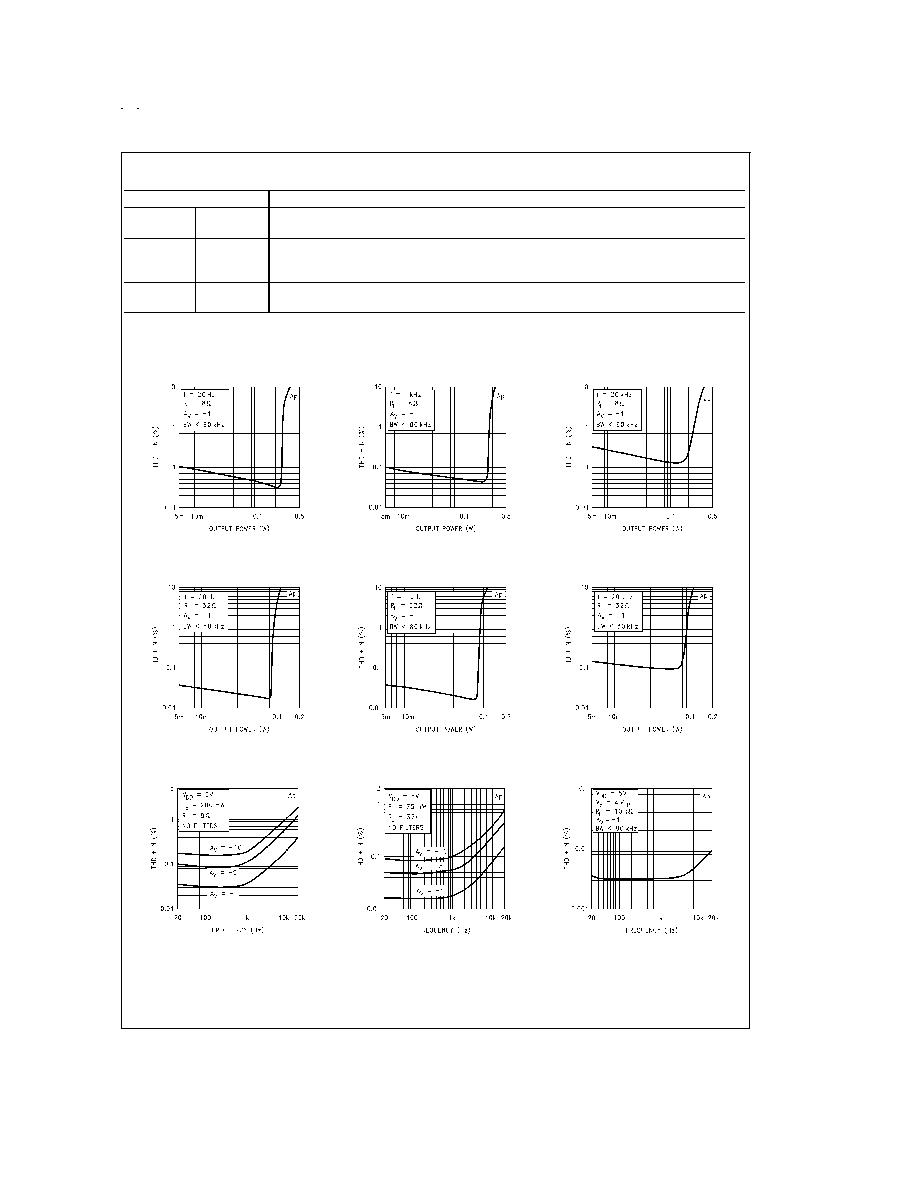
Typical Performance Characteristics
THD + N vs Output Power
DS012343-5
THD + N vs Output Power
DS012343-6
THD + N vs Output Power
DS012343-7
THD + N vs Output Power
DS012343-8
THD + N vs Output Power
DS012343-9
THD + N vs Output Power
DS012343-10
THD + N vs Frequency
DS012343-11
THD + N vs Frequency
DS012343-12
THD + N vs Frequency
DS012343-13
www.national.com
5
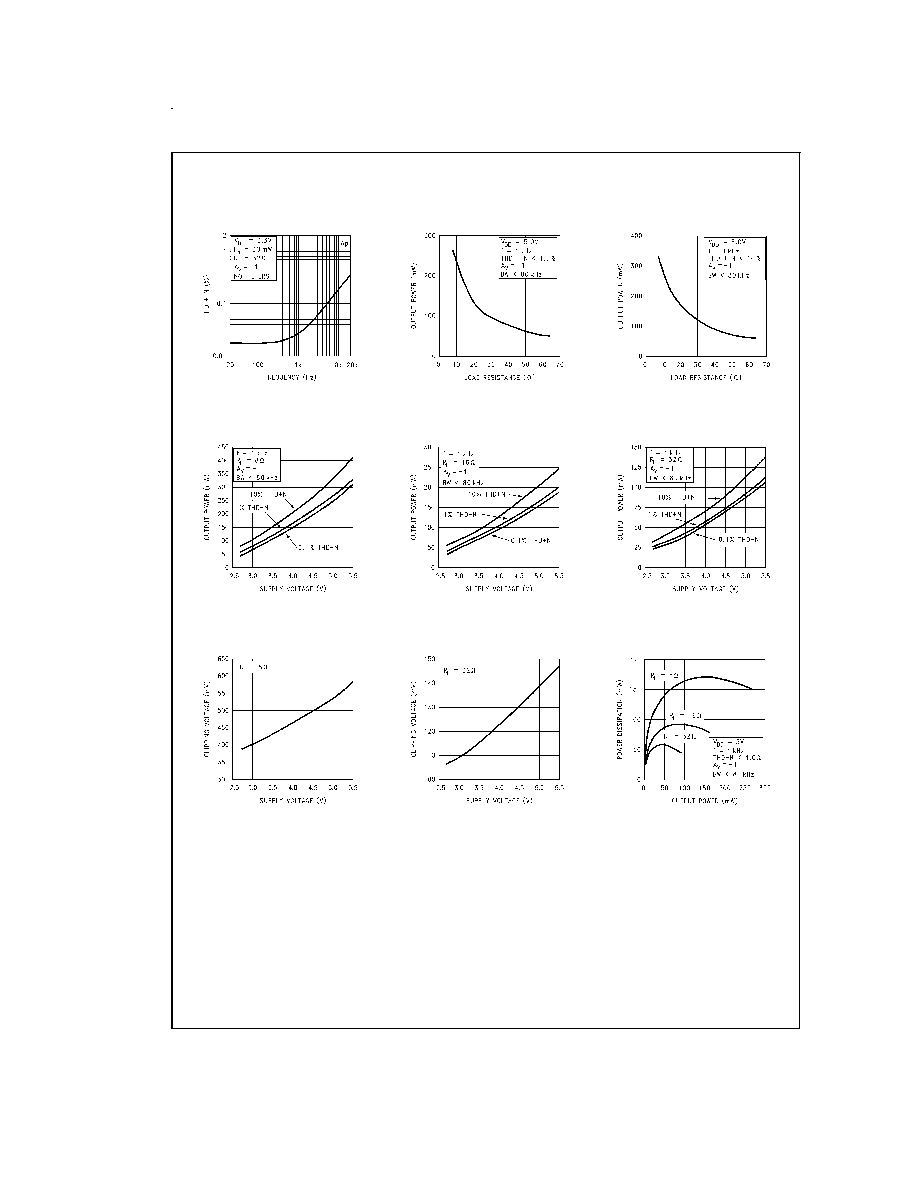
Typical Performance Characteristics
(Continued)
THD + N vs Frequency
DS012343-14
Output Power vs
Load Resistance
DS012343-15
Output Power vs
Load Resistance
DS012343-16
Output Power vs
Supply Voltage
DS012343-17
Output Power vs
Supply Voltage
DS012343-18
Output Power vs
Supply Voltage
DS012343-19
Clipping Voltage vs
Supply Voltage
DS012343-20
Clipping Voltage vs
Supply Voltage
DS012343-21
Power Dissipation vs
Output Power
DS012343-22
www.national.com
6
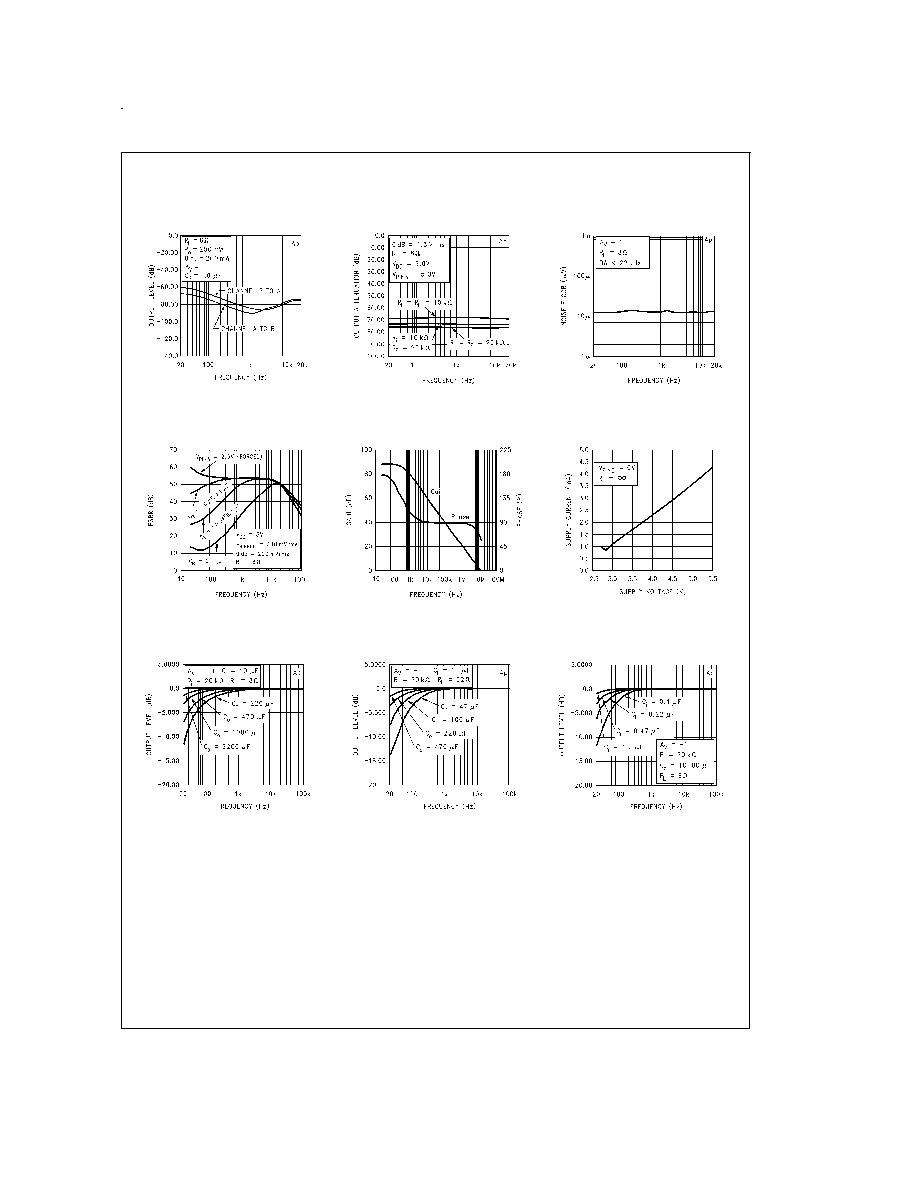
Typical Performance Characteristics
(Continued)
Channel Separation
DS012343-23
Output Attenuation in
Shutdown Mode
DS012343-24
Noise Floor
DS012343-25
Power Supply
Rejection Ratio
DS012343-26
Open Loop
Frequency Response
DS012343-27
Supply Current vs
Supply Voltage
DS012343-28
Frequency Response vs
Output Capacitor Size
DS012343-29
Frequency Response vs
Output Capacitor Size
DS012343-30
Frequency Response vs
Input Capacitor Size
DS012343-31
www.national.com
7
Typical Performance Characteristics
(Continued)
Application Information
SHUTDOWN FUNCTION
In order to reduce power consumption while not in use, the
LM4880 contains a shutdown pin to externally turn off the
amplifier's bias circuitry. This shutdown feature turns the am-
plifier off when a logic high is placed on the shutdown pin.
The trigger point between a logic low and logic high level is
typically half supply. It is best to switch between ground and
the supply to provide maximum device performance. By
switching the shutdown pin to V
DD
, the LM4880 supply cur-
rent draw will be minimized in idle mode. While the device
will be disabled with shutdown pin voltages less than V
DD
,
the idle current may be greater than the typical value of 0.7
µA. In either case, the shutdown pin should be tied to a defi-
nite voltage because leaving the pin floating may result in an
unwanted shutdown condition.
In many applications, a microcontroller or microprocessor
output is used to control the shutdown circuitry which pro-
vides a quick, smooth transition into shutdown. Another solu-
tion is to use a single-pole, single-throw switch in conjunction
with an external pull-up resistor. When the switch is closed,
the shutdown pin is connected to ground and enables the
amplifier. If the switch is open, then the external pull-up re-
sistor will disable the LM4880. This scheme guarantees that
the shutdown pin will not float which will prevent unwanted
state changes.
POWER DISSIPATION
Power dissipation is a major concern when using any power
amplifier and must be thoroughly understood to ensure a
successful design.
Equation (1) states the maximum power
dissipation point for a single-ended amplifier operating at a
given supply voltage and driving a specified output load.
P
DMAX
= (V
DD
)
2
/(2
2
R
L
)
(1)
Since the LM4880 has two operational amplifiers in one
package, the maximum internal power dissipation point is
twice that of the number which results from
Equation (1).
Even with the large internal power dissipation, the LM4880
does not require heat sinking over a large range of ambient
temperatures. From
Equation (1), assuming a 5V power sup-
ply and an 8
load, the maximum power dissipation point is
158 mW per amplifier. Thus the maximum package dissipa-
tion point is 317 mW. The maximum power dissipation point
obtained must not be greater than the power dissipation that
results from
Equation (2):
P
DMAX
= (T
JMAX
-T
A
)/
JA
(2)
For the LM4880 surface mount package,
JA
= 170∞ C/W
and T
JMAX
= 150∞C. Depending on the ambient temperature,
T
A
, of the system surroundings,
Equation (2) can be used to
find the maximum internal power dissipation supported by
the IC packaging. If the result of
Equation (1) is greater than
that of
Equation (2), then either the supply voltage must be
decreased, the load impedance increased, or the ambient
temperature reduced. For the typical application of a 5V
power supply, with an 8
load, the maximum ambient tem-
perature possible without violating the maximum junction
temperature is approximately 96∞C provided that device op-
eration is around the maximum power dissipation point.
Power dissipation is a function of output power and thus, if
typical operation is not around the maximum power dissipa-
tion point, the ambient temperature may be increased ac-
cordingly. Refer to the Typical Performance Characteris-
tics curves for power dissipation information for lower output
powers.
POWER SUPPLY BYPASSING
As with any power amplifier, proper supply bypassing is criti-
cal for low noise performance and high power supply rejec-
tion. The capacitor location on both the bypass and power
supply pins should be as close to the device as possible. As
displayed in the Typical Performance Characteristics sec-
tion, the effect of a larger half supply bypass capacitor is im-
proved low frequency PSRR due to increased half-supply
stability. Typical applications employ a 5V regulator with
10 µF and a 0.1 µF bypass capacitors which aid in supply
stability, but do not eliminate the need for bypassing the sup-
ply nodes of the LM4880. The selection of bypass capaci-
tors, especially C
B
, is thus dependant upon desired low fre-
quency PSRR, click and pop performance as explained in
the section, Proper Selection of External Components
section, system cost, and size constraints.
AUTOMATIC SHUTDOWN CIRCUIT
As shown in
Figure 2, the LM4880 can be set up to automati-
cally shutdown when a load is not connected. This circuit is
based upon a single control pin common in many head-
phone jacks. This control pin forms a normally closed switch
with one of the output pins. The output of this circuit (the volt-
age on pin 5 of the LM4880) has two states based on the
state of the switch. When the switch is open, signifying that
headphones are inserted, the LM4880 should be enabled.
When the switch is closed, the LM4880 should be off to mini-
mize power consumption.
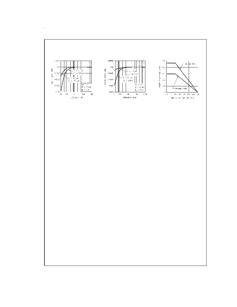
Typical Application
Frequency Response
DS012343-32
Typical Application
Frequency Response
DS012343-33
Power Derating Curve
DS012343-34
www.national.com
8

Application Information
(Continued)
The operation of this circuit is rather simple. With the switch
closed, R
p
and R
o
form a resistor divider which produces a
gate voltage of less than 5 mV. This gate voltage keeps the
NMOS inverter off and R
sd
pulls the shutdown pin of the
LM4880 to the supply voltage. This places the LM4880 in
shutdown mode which reduces the supply current to 0.7 µA
typically. When the switch is open, the opposite condition is
produced. Resistor R
p
pulls the gate of the NMOS high
which turns on the inverter and produces a logic low signal
on the shutdown pin of the LM4880. This state enables the
LM4880 and places the amplifier in its normal mode of op-
eration.
This type of circuit is clearly valuable in portable products
where battery life is critical, but is also benefical for power
conscious designs such as "Green PC's".
AUTOMATIC SWITCHING CIRCUIT
A circuit closely related to the Automatic Shutdown Circuit
is the Automatic Switching Circuit of
Figure 3. The Auto-
matic Switching Circuit utilizes both the input and output of
the NMOS inverter to toggle the states of two different audio
power amplifiers. The LM4880 is used to drive stereo single
ended loads, while the LM4861 drives bridged internal
speakers.
In this application, the LM4880 and LM4861 are never on at
the same time. When the switch inside the headphone jack
is open, the LM4880 is enabled and the LM4861 is disabled
since the NMOS inverter is on. If a headphone jack is not
present, it is assumed that the internal speakers should be
on and thus the voltage on the LM4861 shutdown pin is low
and the voltage at the LM4880 pin is high. This results in the
LM4880 being shutdown and the LM4861 being enabled.
Only one channel of this circuit is shown in
Figure 3 to keep
the drawing simple but the typical application would a
LM4880 driving a stereo external headphone jack and two
LM4861's driving the internal stereo speakers. If only one in-
ternal speaker is required, a single LM4861 can be used as
a summer to mix the left and right inputs into a single mono
channel.
PROPER SELECTION OF EXTERNAL COMPONENTS
Selection of external components when using integrated
power amplifiers is critical to optimize device and system
performance. While the LM4880 is tolerant of external com-
ponent combinations, care must be exercised when choos-
ing component values.
The LM4880 is unity-gain stable which gives a designer
maximum system flexibility. The LM4880 should be used in
low gain configurations to minimize THD + N values, and
maximize the signal to noise ratio. Low gain configurations
require large input signals to obtain a given output power. In-
put signals equal to or greater than 1 Vrms are available
from sources such as audio codecs. Please refer to the sec-
tion, Audio Power Amplifier Design, for a more complete
explanation of proper gain selection.
Besides gain, one of the major design considerations is the
closed-loop bandwidth of the amplifier. To a large extent, the
bandwidth is dictated by the choice of external components
shown in
Figure 1. Both the input coupling capacitor, C
i
, and
the output coupling capacitor, C
o
, form first order high pass
filters which limit low frequency response. These values
should be chosen based on needed frequency response for
a few distinct reasons.
Selection of Input and Output Capacitor Size
Large input and output capacitors are both expensive and
space hungry for portable designs. Clearly a certain sized
capacitor is needed to couple in low frequencies without se-
vere attenuation. But in many cases the transducers used in
portable systems, whether internal or external, have little
ability to reproduce signals below 100 Hz≠150 Hz. Thus us-
ing large input and output capacitors may not increase sys-
tem performance.
In addition to system cost and size, click and pop perfor-
mance is effected by the size of the input coupling capacitor,
C
i
. A larger input coupling capacitor requires more charge to
reach its quiescent DC voltage (normally 1/2 V
DD
.) This
charge comes from the output via the feedback and is apt to
create pops upon device enable. Thus, by minimizing the ca-
pacitor size based on necessary low frequency response,
turn-on pops can be minimized.
Besides minimizing the input and output capacitor sizes,
careful consideration should be paid to the bypass capacitor
size. The bypass capacitor, C
B
, is the most critical compo-
nent to minimize turn-on pops since it determines how fast
the LM4880 turns on. The slower the LM4880's outputs
ramp to their quiescent DC voltage (nominally 1/2 V
DD
), the
smaller the turn-on pop. Choosing C
B
equal to 1.0 µF along
with a small value of C
i
(in the range of 0.1 µF to 0.39 µF),
should produce a virtually clickless and popless shutdown
function. While the device will function properly, (no oscilla-
tions or motorboating), with C
B
equal to 0.1 µF, the device
will be much more susceptible to turn-on clicks and pops.
Thus, a value of C
B
equal to 1.0 µF or larger is recom-
mended in all but the most cost sensitive designs.
AUDIO POWER AMPLIFIER DESIGN
Design a Dual 200 mW/8
Audio Amplifier
Given:
Power Output:
200 mWrms
Load Impedance:
8
Input Level:
1 Vrms (max)
Input Impedance:
20 k
Bandwidth:
100 Hz≠20 kHz
±
0.50 dB
A designer must first determine the needed supply rail to ob-
tain the specified output power. Calculating the required sup-
ply rail involves knowing two parameters, V
opeak
and also the
dropout voltage. As shown in the Typical Performance
Curves, the dropout voltage is typically 0.5V. V
opeak
can be
determined from
Equation (3).
(3)
For 200 mW of output power into an 8
load, the required
V
opeak
is 1.79V. Since this is a single supply application, the
minimum supply voltage is twice the sum of V
opeak
and V
od
.
Since 5V is a standard supply voltage in most applications, it
is chosen for the supply rail. Extra supply voltage creates
headroom that allows the LM4880 to reproduce peaks in ex-
cess of 200 mW without clipping the signal. At this time, the
designer must make sure that the power supply choice along
with the output impedance does not violate the conditions
explained in the Power Dissipation section. Remember that
the maximum power dissipation value from
Equation (1)
must be multiplied by two since there are two independent
amplifiers inside the package.
Once the power dissipation equations have been addressed,
the required gain can be determined from
Equation (4).
www.national.com
9

Application Information
(Continued)
(4)
A
V
= -R
F
/R
i
(5)
From
Equation (4), the minimum gain is::
A
V
= -1.26
Since the desired input impedance was 20 k
, and with a
gain of -1.26, a value of 27 k
is designated for R
f
, assum-
ing 5% tolerance resistors. This combination results in a
nominal gain of -1.35. The final design step is to address the
bandwidth requirements which must be stated as a pair of
-3 dB frequency points. Five times away from a -3 dB point
is 0.17 dB down from passband response assuming a single
pole roll-off. As stated in the External Components section,
both R
i
in conjunction with C
i
, and C
o
with R
L
, create first or-
der high pass filters. Thus to obtain the desired frequency
low response of 100 Hz within
±
0.5 dB, both poles must be
taken into consideration. The combination of two single order
filters at the same frequency forms a second order response.
This results in a signal which is down 0.34 dB at five times
away from the single order filter -3 dB point. Thus, a fre-
quency of 20 Hz is used in the following equations to ensure
that the response if better than 0.5 dB down at 100 Hz.
C
i
1/(2
*
20k
*
20Hz) = 0.397 µF; use 0.39 µF
C
o
1/(2
*
8
*
20Hz) = 995 µF; use 1000 µF
The high frequency pole is determined by the product of the
desired high frequency pole, f
H
, and the closed-loop gain,
A
V
. With a closed-loop gain magnitude of 1.35 and f
H
= 100
kHz, the resulting GBWP = 135 kHz which is much smaller
than the LM4880 GBWP of 12.5 MHz. This figure displays
that if a designer has a need top design an amplifier with a
higher gain, the LM4880 can still be used without running
into bandwidth limitations.
www.national.com
10
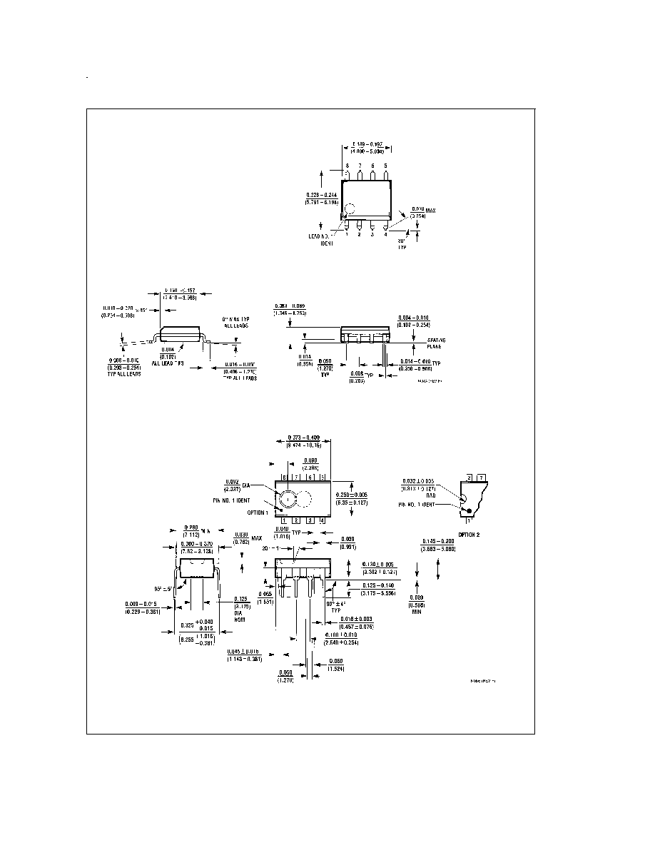
Physical Dimensions
inches (millimeters) unless otherwise noted
8-Lead (0.150" Wide) Molded Small Outline Package, JEDEC
Order Number LM4880M
NS Package Number M08A
8-Lead (0.300" Wide) Molded Dual-In-Line Package
Order Number LM4880N
NS Package Number N08E
www.national.com
11

Notes
LIFE SUPPORT POLICY
NATIONAL'S PRODUCTS ARE NOT AUTHORIZED FOR USE AS CRITICAL COMPONENTS IN LIFE SUPPORT
DEVICES OR SYSTEMS WITHOUT THE EXPRESS WRITTEN APPROVAL OF THE PRESIDENT AND GENERAL
COUNSEL OF NATIONAL SEMICONDUCTOR CORPORATION. As used herein:
1. Life support devices or systems are devices or
systems which, (a) are intended for surgical implant
into the body, or (b) support or sustain life, and
whose failure to perform when properly used in
accordance with instructions for use provided in the
labeling, can be reasonably expected to result in a
significant injury to the user.
2. A critical component is any component of a life
support device or system whose failure to perform
can be reasonably expected to cause the failure of
the life support device or system, or to affect its
safety or effectiveness.
National Semiconductor
Corporation
Americas
Tel: 1-800-272-9959
Fax: 1-800-737-7018
Email: support@nsc.com
National Semiconductor
Europe
Fax: +49 (0) 1 80-530 85 86
Email: europe.support@nsc.com
Deutsch Tel: +49 (0) 1 80-530 85 85
English
Tel: +49 (0) 1 80-532 78 32
FranÁais Tel: +49 (0) 1 80-532 93 58
Italiano
Tel: +49 (0) 1 80-534 16 80
National Semiconductor
Asia Pacific Customer
Response Group
Tel: 65-2544466
Fax: 65-2504466
Email: sea.support@nsc.com
National Semiconductor
Japan Ltd.
Tel: 81-3-5639-7560
Fax: 81-3-5639-7507
www.national.com
LM4880
Boomer
Audio
Power
Amplifier
Series
Dual
250
mW
Audio
Power
Amplifier
with
Shutdown
Mode
National does not assume any responsibility for use of any circuitry described, no circuit patent licenses are implied and National reserves the right at any time without notice to change said circuitry and specifications.