 | –≠–ª–µ–∫—Ç—Ä–æ–Ω–Ω—ã–π –∫–æ–º–ø–æ–Ω–µ–Ω—Ç: LM4882 | –°–∫–∞—á–∞—Ç—å:  PDF PDF  ZIP ZIP |
LM4882
250mW Audio Power Amplifier with Shutdown Mode
General Description
The LM4882 is a single-ended audio power amplifier ca-
pable of delivering 250 mW of continuous average power
into an 8
load with 1% (THD + N) from a 5V power supply.
Boomer
Æ
audio power amplifiers were designed specifically
to provide high quality output power with a minimal amount
of external components using surface mount packaging.
Since the LM4882 does not require bootstrap capacitors or
snubber networks, it is optimally suited for low-power por-
table systems.
The LM4882 features an externally controlled, low power
consumption shutdown mode which is virtually clickless and
popless, as well as an internal thermal shutdown protection
mechanism.
The unity-gain stable LM4882 can be configured by external
gain-setting resistors.
Key Specifications
n
THD + N at 1 kHz at 250 mW
continuous average output
power into 8
1.0% (max)
n
Output Power at 1% THD + N
at 1kHz into 4
380mW (typ)
n
THD + N at 1 kHz at 85 mW
continuous average output
power into 32
0.1% (typ)
n
Shutdown Current
0.7 µA (typ)
Features
n
MSOP surface mount packaging
n
"Click and Pop" Suppression Circuitry
n
Supply voltages from 2.4V≠5.5V
n
Operating Temperature -40∞C to 85∞C
n
Unity-gain stable
n
External gain configuration capability
n
No bootstrap capacitors, or snubber circuits are
necessary
Applications
n
Personal Computers
n
Cellular Phones
n
General Purpose Audio
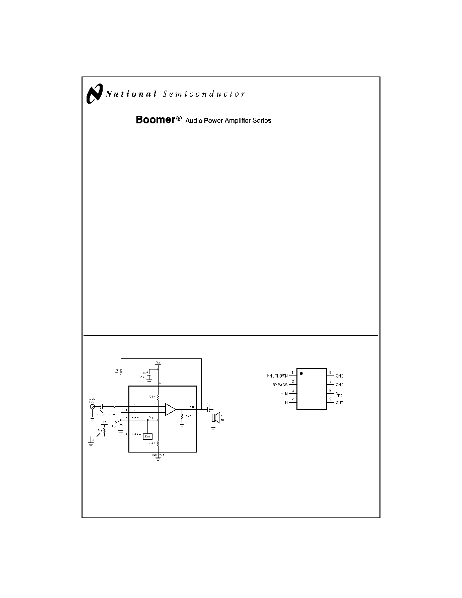
Typical Application
Connection Diagram
Boomer
Æ
is a registered trademark of National Semiconductor Corporation.
DS100030-1
*Refer to the Application Information Section for information concerning
proper selection of the input and output coupling capacitors.
FIGURE 1. Typical Audio Amplifier Application Circuit
MSOP and SOIC Package
DS100030-2
Top View
Order Number LM4882MM or LM4882M
See NS Package Number MUA08A or M08A
January 1998
LM4882
250mW
Audio
Power
Amplifier
with
Shutdown
Mode
© 1998 National Semiconductor Corporation
DS100030
www.national.com
Absolute Maximum Ratings
(Note 1)
If Military/Aerospace specified devices are required,
please contact the National Semiconductor Sales Office/
Distributors for availability and specifications.
Supply Voltage
6.0 V
Storage Temperature
-65∞C to +150∞C
Input Voltage
-0.3V to V
DD
+ 0.3V
Power Dissipation (Note 3)
Internally limited
ESD Susceptibility (Note 4)
2000V
PIn 5
1500V
Junction Temperature
150∞C
Soldering Information
Small Outline Package
Vapor Phase (60 seconds)
215∞C
Infrared (15 seconds)
220∞C
See AN-450
Surface Mounting and their Effects on
Product Reliability
for other methods of soldering surface
mount devices.
Thermal Resistance
JC
(MSOP)
56∞C/W
JA
(MSOP)
210∞C/W
JC
(SOP)
35∞C/W
JA
(SOP)
170∞C/W
Operating Ratings
Temperature Range
T
MIN
T
A
T
MAX
-40∞C
T
A
85∞C
Supply Voltage
2.4V
V
DD
5.5V
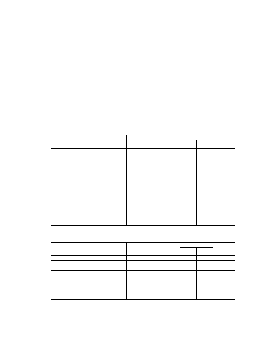
Electrical Characteristics
(Notes 1, 2)
The following specifications apply for V
DD
= 5V unless otherwise specified. Limits apply for T
A
= 25∞C.
Symbol
Parameter
Conditions
LM4882
Units
(Limits)
Typical
(Note 5)
Limit
(Note 6)
I
DD
Quiescent Current
V
IN
= 0V, I
O
= 0A
2
4.0
mA (max)
I
SD
Shutdown Current
V
pin1
= V
DD
0.5
5
µA (max)
V
OS
Offset Voltage
V
IN
= 0V
5
50
mV (max)
P
O
Output Power
THD + N = 1% (max); f = 1 kHz;
R
L
= 4
380
mW
R
L
= 8
270
250
mW (min)
R
L
= 32
95
mW
THD + N = 10%; f = 1 kHz
R
L
= 4
480
mW
R
L
= 8
325
mW
R
L
= 32
125
mW
THD + N
Total Harmonic Distortion + Noise
R
L
= 8
, P
O
= 250 mWrms;
0.5
%
R
L
= 32
, P
O
= 85 mWrms;
0.1
%
f = 1 kHz
PSRR
Power Supply Rejection Ratio
V
pin3
= 2.5V, V
ripple
= 200 mVrms,
f = 120 Hz
50
dB
Electrical Characteristics
(Notes 1, 2)
The following specifications apply for V
DD
= 3V unless otherwise specified. Limits apply for T
A
= 25∞C.
Symbol
Parameter
Conditions
LM4882
Units
(Limits)
Typical
(Note 5)
Limit
(Note 6)
I
DD
Quiescent Current
V
IN
= 0V, I
O
= 0A
1.2
mA
I
SD
Shutdown Current
V
pin1
= V
DD
0.3
µA
V
OS
Offset Voltage
V
IN
= 0V
5
mV
P
O
Output Power
THD + N = 1% (max); f = 1 kHz
R
L
= 8
80
mW
R
L
= 32
30
mW
THD + N = 10%; f = 1 kHz
R
L
= 8
105
mW
R
L
= 32
40
mW
www.national.com
2
Electrical Characteristics
(Notes 1, 2) (Continued)
The following specifications apply for V
DD
= 3V unless otherwise specified. Limits apply for T
A
= 25∞C.
Symbol
Parameter
Conditions
LM4882
Units
(Limits)
Typical
(Note 5)
Limit
(Note 6)
THD + N
Total Harmonic Distortion + Noise
R
L
= 8
, P
O
= 70 mWrms;
0.25
%
R
L
= 32
, P
O
= 30 mWrms;
0.3
%
f = 1 kHz
PSRR
Power Supply Rejection Ratio
V
pin3
= 2.5V, V
ripple
= 200 mVrms,
f = 120 Hz
50
dB
Note 1: All voltages are measured with respect to the ground pin, unless otherwise specified.
Note 2:
Absolute Maximum Ratings indicate limits beyond which damage to the device may occur. Operating Ratings indicate conditions for which the device is func-
tional, but do not guarantee specific performance limits.
Electrical Characteristics state DC and AC electrical specifications under particular test conditions which guar-
antee specific performance limits. This assumes that the device is within the Operating Ratings. Specifications are not guaranteed for parameters where no limit is
given, however, the typical value is a good indication of device performance.
Note 3: The maximum power dissipation must be derated at elevated temperatures and is dictated by T
JMAX
,
JA
, and the ambient temperature T
A
. The maximum
allowable power dissipation is P
DMAX
= (T
JMAX
- T
A
)/
JA
. For the LM4882, T
JMAX
= 150∞C, and the typical junction-to-ambient thermal resistance, when board
mounted, is 210∞C/W for the MUA08A Package and 170∞C/W for the M08A Package.
Note 4: Human body model, 100 pF discharged through a 1.5 k
resistor.
Note 5: Typicals are measured at 25∞C and represent the parametric norm.
Note 6: Limits are guaranteed to National's AOQL (Average Outgoing Quality Level).
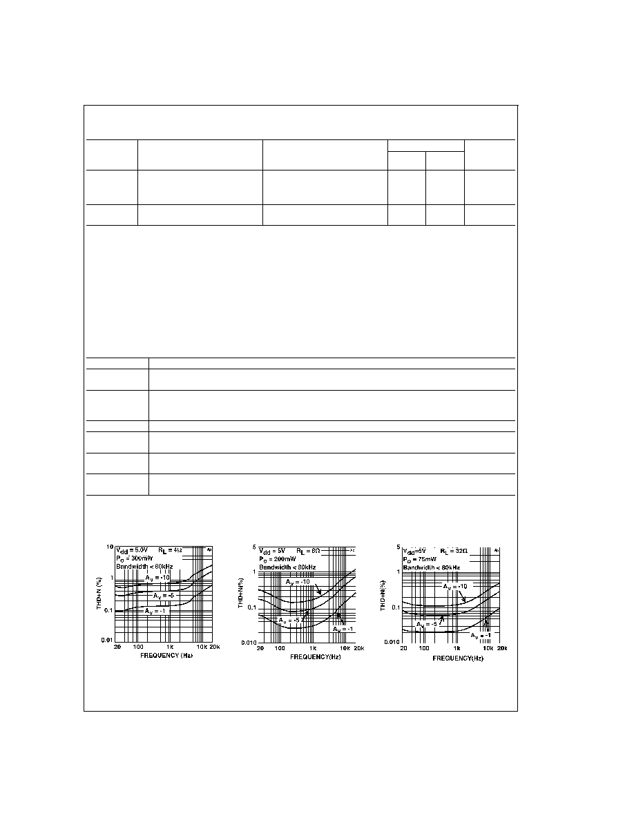
External Components Description
(Refer to
Figure 1)
Components
Functional Description
1. R
i
Inverting input resistance which sets the closed-loop gain in conjunction with R
f
. This resistor also forms a
high pass filter with C
i
at f
c
= 1 / (2
R
i
C
i
).
2. C
i
Input coupling capacitor which blocks the DC voltage at the amplifier's input terminals. Also creates a
highpass filter with R
i
at f
c
= 1 / (2
R
i
C
i
). Refer to the section, Proper Selection of External Components,
for an explanation of how to determine the values of C
i
.
3. R
f
Feedback resistance which sets closed-loop gain in conjunction with R
i
.
4. C
S
Supply bypass capacitor which provides power supply filtering. Refer to the Application Information section
for proper placement and selection of the supply bypass capacitor.
5. C
B
Bypass pin capacitor which provides half-supply filtering. Refer to the section, Proper Selection of External
Components, for information concerning proper placement and selection of C
B
.
6. C
O
Output coupling capacitor which blocks the DC voltage at the amplifier's output. Forms a high pass filter wth
R
L
at f
O
= 1 / (2
R
L
C
O
).
Typical Performance Characteristics
THD+N vs Frequency
DS100030-26
THD+N vs Frequency
DS100030-9
THD+N vs Frequency
DS100030-10
3
www.national.com
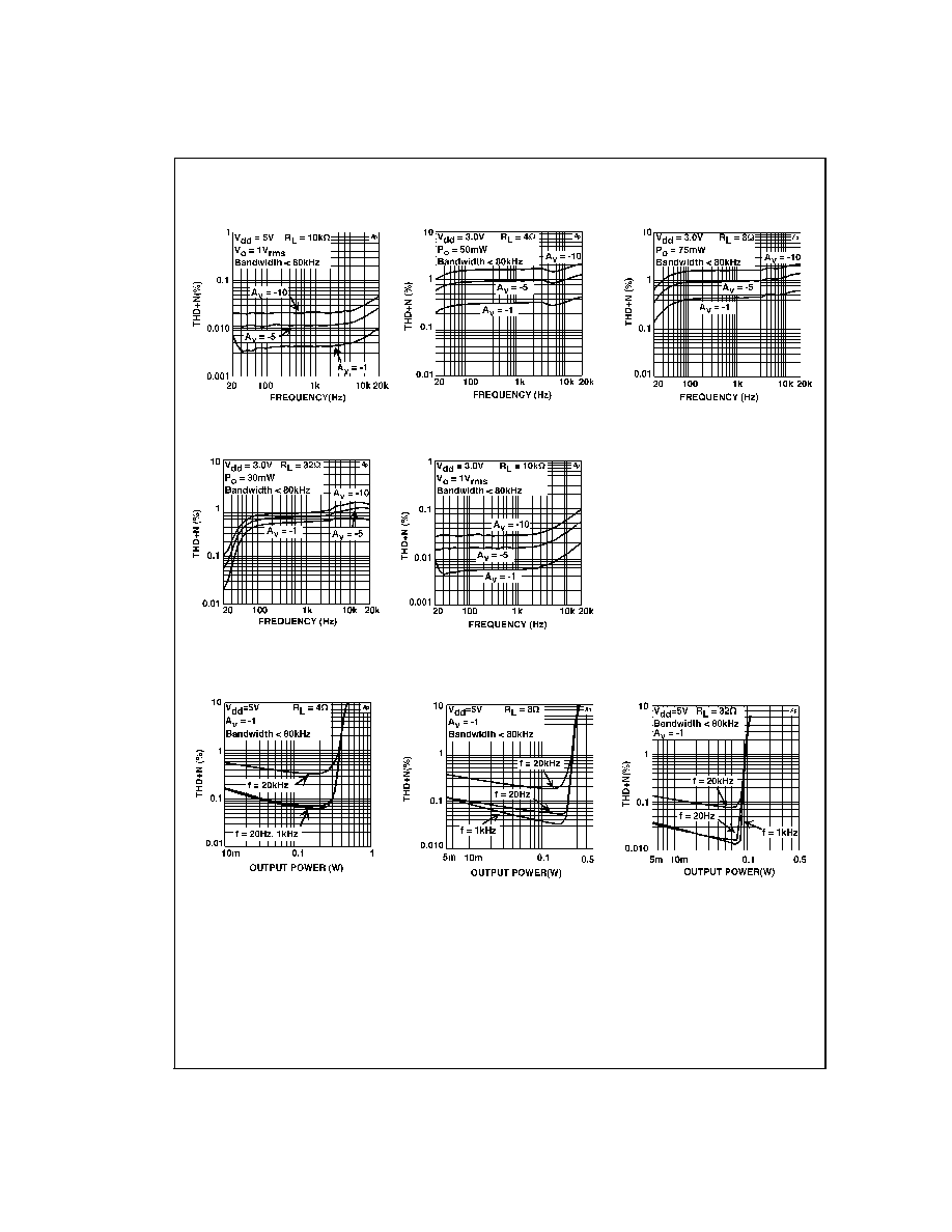
Typical Performance Characteristics
(Continued)
THD+N vs Frequency
DS100030-11
THD+N vs Frequency
DS100030-23
THD+N vs Frequency
DS100030-22
THD+N vs Frequency
DS100030-24
THD+N vs Frequency
DS100030-25
THD+N vs
Output Power
DS100030-29
THD+N vs
Output Power
DS100030-4
THD+N vs
Output Power
DS100030-8
www.national.com
4
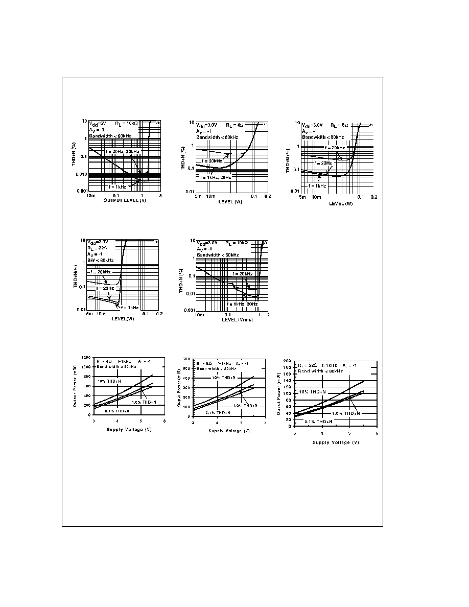
Typical Performance Characteristics
(Continued)
THD+N vs
Output Power
DS100030-30
THD+N vs
Output Power
DS100030-18
THD+N vs
Output Power
DS100030-19
THD+N vs
Output Power
DS100030-20
THD+N vs
Output Power
DS100030-21
Output Power vs
Supply Voltage
DS100030-12
Output Power vs
Supply Voltage
DS100030-13
Output Power vs
Supply Voltage
DS100030-14
5
www.national.com