 | –≠–ª–µ–∫—Ç—Ä–æ–Ω–Ω—ã–π –∫–æ–º–ø–æ–Ω–µ–Ω—Ç: LM4883SQ | –°–∫–∞—á–∞—Ç—å:  PDF PDF  ZIP ZIP |
Document Outline
- LM4883 Boomer (R) Audio Power Amplifier Series
- General Description
- Key Specifications
- Features
- Applications
- Connection Diagrams
- Typical Application
- Absolute Maximum Ratings
- Operating Ratings
- Electrical Characteristics (5V) (Notes , , )
- Electrical Characteristics for Bridged-Mode Operation (5V) (Notes , , )
- Electrical Characteristics for Single-Ended Operation (5V) (Notes , , )
- Electrical Characteristics (3V) (Notes , , )
- Electrical Characteristics for Bridged-Mode Operation (3V) (Notes , , )
- Electrical Characteristics for Single-Ended Operation (3V) (Notes , , )
- Typical Performance Characteristics
- Application Information
- Demonstration Board Layout
- Bill of Materials
- Physical Dimensions
LM4883
Dual 2.1W Audio Amplifier Plus Stereo Headphone
Function
General Description
The LM4883 is a dual bridge-connected audio power ampli-
fier which, when connected to a 5V supply, will deliver 2.1W
to a 4
load (Note 1) or 2.4W to a 3 load (Note 2) with less
than 1.0% THD+N. In addition, the headphone input pin
allows the amplifiers to operate in single-ended mode when
driving stereo headphones. A MUX control pin allows selec-
tion between the two stereo sets of amplifier inputs. The
MUX control can also be used to select two different closed-
loop responses.
Boomer audio power amplifiers were designed specifically to
provide high quality output power from a surface mount
package while requiring few external components. To sim-
plify audio system design, the LM4883SQ combines dual
bridge speaker amplifiers and stereo headphone amplifiers
on one chip.
The LM4883SQ features an internally controlled, low-power
consumption shutdown mode, a stereo headphone amplifier
mode, and thermal shutdown protection. It also utilizes cir-
cuitry to reduce "clicks and pops" during device turn-on.
Note 1: An LM4883SQ that has been properly mounted to a circuit board
will deliver 2.1W into 4
. See the Application Information sections for further
information concerning the LM4883SQ.
Note 2: An LM4883SQ that has been properly mounted to a circuit board
and forced-air cooled will deliver 2.4W into 3
.
Key Specifications
j
P
O
at 1% THD+N
R
L
= 3
2.4W (typ)
R
L
= 4
2.1W (typ)
R
L
= 8
1.3W (typ)
j
Single-ended mode THD+N
at 75mW into 32
(5V, 1kHz)
0.01% (typ)
j
Shutdown current
0.04µA (typ)
j
Supply voltage range
2.4V to 5.5V
j
PSRR at 217Hz
85dB (typ)
Features
n
Input mux control and two separate inputs per channel
n
Stereo headphone amplifier mode
n
Improved "click and pop" suppression circuitry
n
Thermal shutdown protection circuitry
n
PCB area-saving SQ package
Applications
n
Multimedia monitors
n
Portable and desktop computers
n
Portable audio systems
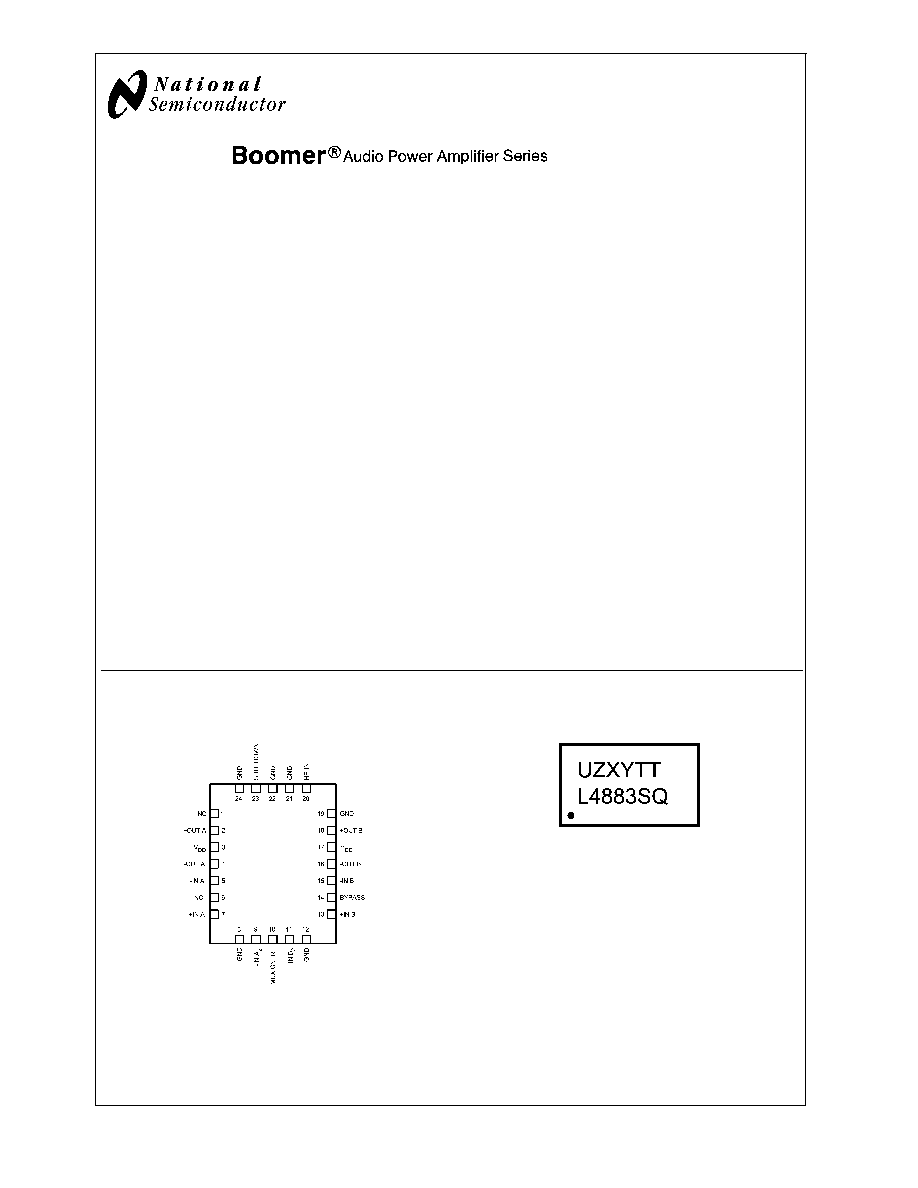
Connection Diagrams
LM4883SQ
LM4883SQ Top Mark
200887A3
Top View
Order Number LM4883SQ
See NS Package Number SQA24B
200887C6
Top View
U = Fab Code
Z = Assembly Plant Code
XY = Date Code
TT = Die Traceability
Boomer
Æ
is a registered trademark of National Semiconductor Corporation.
November 2004
LM4883
Dual
2.1W
Audio
Amplifier
Plus
Stereo
Headphone
Function
© 2004 National Semiconductor Corporation
DS200887
www.national.com
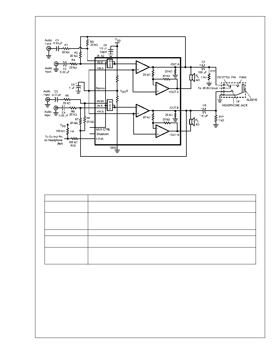
Typical Application
External Components Description
(Refer to Figure 1)
Components
Functional Description
1.
R1, 4, 5, 6
The inverting input resistance R1, along with R
3
, set the closed-loop gain. R
1
, along with C
1
,
form a high pass filter with f
c
= 1/(2
R
1
C
1
).
2.
C1, 2, 3, 4
The input coupling capacitor blocks DC voltage at the amplifier's input terminals. C
1
, along with
R
1
, create a highpass filter with f
c
= 1/(2
R
1
C
1
). Refer to the section, SELECTING PROPER
EXTERNAL COMPONENTS, for an explanation of determining the value of C
1
.
3.
R2, 3, 7, 8
The feedback resistance, along with R
1
sets the closed-loop gain.
4.
C6
The supply bypass capacitor. Refer to the POWER SUPPLY BYPASSING section for
information about properly placing, and selecting the value of, this capacitor.
5.
C5
The capacitor, C
5
, filters the half-supply voltage present on the BYPASS pin. Refer to the
SELECTING PROPER EXTERNAL COMPONENTS section for information concerning proper
placement and selecting C
5
's value.
200887A1
FIGURE 1. Typical Audio Amplifier Application Circuit
LM4883
www.national.com
2
Absolute Maximum Ratings
(Note 3)
If Military/Aerospace specified devices are required,
please contact the National Semiconductor Sales Office/
Distributors for availability and specifications.
Supply Voltage
6.0V
Storage Temperature
-65∞C to +150∞C
Input Voltage
-0.3V to V
DD
+0.3V
Power Dissipation (Note 4)
Internally limited
ESD Susceptibility (Note 5)
2000V
ESD Susceptibility (Note 6)
200V
Junction Temperature
150∞C
Solder Information
Small Outline Package
Vapor Phase (60 sec.)
215∞C
Infrared (15 sec.)
220∞C
Thermal Resistance
JC
(typ) -- SQA24B
3∞C/W
JA
(typ) -- SQA24B
42∞C/W
Operating Ratings
Temperature Range
T
MIN
T
A
T
MAX
-40∞C
T
A
85∞C
Supply Voltage
2.4V
V
DD
5.5V
Electrical Characteristics (5V)
(Notes 3, 7, 13)
The following specifications apply for V
DD
= 5V unless otherwise noted. Limits apply for T
A
= 25∞C.
Symbol
Parameter
Conditions
LM4883
Units
(Limits)
Typical
Limit
(Note 8)
(Note 9)
V
DD
Supply Voltage
2.4
V (min)
5.5
V (max)
I
DD
Quiescent Power Supply Current
V
IN
= 0V, I
O
= 0A (Note 10) , HP-IN = 0V
6
10
mA (max)
V
IN
= 0V, I
O
= 0A (Note 10) , HP-IN = 4V
3.0
6
mA (min)
I
SD
Shutdown Current
V
DD
applied to the SHUTDOWN pin
0.04
2
µA (max)
V
IH
Headphone High Input Voltage
3.7
4
V (min)
V
IL
Headphone Low Input Voltage
2.6
0.8
V (max)
V
IHSD
Shutdown High Input Voltage
0.7V
DD
V (min)
V
ILSD
Shutdown Low Input Voltage
0.3V
DD
V (max)
T
WU
Turn On Time
1µF Bypass Cap (C5)
140
ms
Electrical Characteristics for Bridged-Mode Operation (5V)
(Notes 3, 7, 13)
The following specifications apply for V
DD
= 5V unless otherwise specified. Limits apply for T
A
= 25∞C.
Symbol
Parameter
Conditions
LM4883
Units
(Limits)
Typical
Limit
(Note 8)
(Note 9)
V
OS
Output Offset Voltage
V
IN
= 0V
5
45
mV (max)
P
O
Output Power (Note 11)
THD+N = 1%, f = 1kHz (Note 12)
LM4883SQ, R
L
= 3
2.4
W
LM4883SQ, R
L
= 4
2.1
W
LM4883SQ, R
L
= 8
1.3
1.0
W (min)
THD+N = 10%, f = 1kHz (Note 12)
LM4883SQ, R
L
= 3
3.0
W
LM4883SQ, R
L
= 4
2.5
W
LM4883SQ, R
L
= 8
1.7
W
THD+N
Total Harmonic Distortion+Noise
1kHz, A
VD
= 2
LM4883SQ, R
L
= 4
, P
O
= 1W
0.10
%
LM4883SQ, R
L
= 8
, P
O
= .4W
0.06
%
LM4883
www.national.com
3
Electrical Characteristics for Bridged-Mode Operation (5V)
(Notes 3, 7,
13) (Continued)
The following specifications apply for V
DD
= 5V unless otherwise specified. Limits apply for T
A
= 25∞C.
Symbol
Parameter
Conditions
LM4883
Units
(Limits)
Typical
Limit
(Note 8)
(Note 9)
PSRR
Power Supply Rejection Ratio
Input Floating, 217Hz
V
ripple
= 200mV
p-p
C
B
= 1µF, R
L
= 8
85
dB
Input Floating, 1kHz
V
ripple
= 200mV
p-p
C
B
= 1µF, R
L
= 8
80
dB
Input grounded, 217Hz
V
ripple
= 200mV
p-p
C
B
= 1µF, R
L
= 8
65
dB
Input grounded, 1kHz
V
ripple
= 200mV
p-p
C
B
= 1µF, R
L
= 8
70
dB
X
TALK
Channel Separation
f = 1kHz, C
B
= 1.0µF
82
dB
V
NO
Output Noise Voltage
1kHz, A-weighted
21
µV
Electrical Characteristics for Single-Ended Operation (5V)
(Notes 3, 7, 13)
The following specifications apply for V
DD
= 5V unless otherwise specified. Limits apply for T
A
= 25∞C.
Symbol
Parameter
Conditions
LM4883
Units
(Limits)
Typical
Limit
(Note 8)
(Note 9)
P
O
Output Power
THD+N = 0.5%, f = 1 kHz, R
L
= 32
90
75
mW (min)
THD+N = 1%, f = 1 kHz, R
L
= 8
325
mW
THD+N = 10%, f = 1 kHz, R
L
= 8
400
mW
THD+N
Total Harmonic Distortion+Noise
P
O
= 20mW, 1kHz, R
L
= 32
0.015
%
PSRR
Power Supply Rejection Ratio
Input Floating, 217Hz
V
ripple
= 200mV
p-p
C
B
= 1µF, R
L
= 8
70
dB
Input Floating, 1kHz
V
ripple
= 200mV
p-p
C
B
= 1µF, R
L
= 8
72
dB
Input grounded, 217Hz
V
ripple
= 200mV
p-p
C
B
= 1µF, R
L
= 8
65
dB
Input grounded, 1kHz
V
ripple
= 200mV
p-p
C
B
= 1µF, R
L
= 8
70
dB
X
TALK
Channel Separation
f = 1kHz, C
B
= 1.0µF
80
dB
V
NO
Output Noise Voltage
1kHz, A-weighted
11
µV
LM4883
www.national.com
4
Electrical Characteristics (3V)
(Notes 3, 7, 13)
The following specifications apply for V
DD
= 3V unless otherwise noted. Limits apply for T
A
= 25∞C.
Symbol
Parameter
Conditions
LM4883
Units
(Limits)
Typical
Limit
(Note 8)
(Note 9)
I
DD
Quiescent Power Supply Current
V
IN
= 0V, I
O
= 0A (Note 10) , HP-IN = 0V
4.5
mA
V
IN
= 0V, I
O
= 0A (Note 10) , HP-IN = 4V
2.5
mA
I
SD
Shutdown Current
V
DD
applied to the SHUTDOWN pin
0.01
µA
V
IH
Headphone High Input Voltage
2.2
V
V
IL
Headphone Low Input Voltage
1.5
V
V
IHSD
Shutdown High Input Voltage
0.7V
DD
V (min)
V
ILSD
Shutdown Low Input Voltage
0.3V
DD
V (max)
T
WU
Turn On Time
1µF Bypass Cap (C5)
140
ms
Electrical Characteristics for Bridged-Mode Operation (3V)
(Notes 3, 7, 13)
The following specifications apply for V
DD
= 3V unless otherwise specified. Limits apply for T
A
= 25∞C.
Symbol
Parameter
Conditions
LM4883
Units
(Limits)
Typical
Limit
(Note 8)
(Note 9)
V
OS
Output Offset Voltage
V
IN
= 0V
5
mV
P
O
Output Power (Note 11)
THD+N = 1%, f = 1kHz (Note 12)
LM4883SQ, R
L
= 3
.82
W
LM4883SQ, R
L
= 4
.70
W
LM4883SQ, R
L
= 8
.43
W
THD+N = 10%, f = 1kHz (Note 12)
LM4883SQ, R
L
= 3
1.0
W
LM4883SQ, R
L
= 4
.85
W
LM4883SQ, R
L
= 8
.53
W
THD+N
Total Harmonic Distortion+Noise
1kHz
LM4883SQ, R
L
= 4
, P
O
= 280mW
0.1
%
LM4883SQ, R
L
= 8
, P
O
= 200mW
0.05
%
PSRR
Power Supply Rejection Ratio
Input Floating, 217Hz
V
ripple
= 200mV
p-p
C
B
= 1µF, R
L
= 8
90
dB
Input Floating, 1kHz
V
ripple
= 200mV
p-p
C
B
= 1µF, R
L
= 8
80
dB
Input grounded, 217Hz
V
ripple
= 200mV
p-p
C
B
= 1µF, R
L
= 8
65
dB
Input grounded, 1kHz
V
ripple
= 200mV
p-p
C
B
= 1µF, R
L
= 8
73
dB
X
TALK
Channel Separation
f = 1kHz, C
B
= 1.0µF
85
dB
V
NO
Output Noise Voltage
1kHz, A-weighted
21
µV
LM4883
www.national.com
5