 | ÐлекÑÑоннÑй компоненÑ: LM4888SQX | СкаÑаÑÑ:  PDF PDF  ZIP ZIP |
LM4888 Boomer ® Audio Power Amplifier Series Dual 2.1W Audio Amplifier Plus Stereo Headphone & 3D Enhancement
LM4888
Dual 2.1W Audio Amplifier Plus Stereo Headphone & 3D
Enhancement
General Description
The LM4888 is a dual bridge-connected audio power ampli-
fier which, when connected to a 5V supply, will deliver 2.1W
to a 4
load (Note 1) or 2.4W to a 3 load (Note 2) with less
than 1.0% THD+N.
A user selectable "National 3D Enhancement" mode pro-
vides enhanced stereo imaging.
The LM4888SQ also has two separate HP (headphone)
enable inputs, each having different logic level thresholds.
Either HP enable input activates the single ended head-
phone mode and disables the BTL output mode. The HP
Sense input is for use with a normal stereo headphone jack.
The remaining input, HP Logic, accepts standard logic level
thresholds.
Boomer audio power amplifiers were designed specifically to
provide high quality output power from a surface mount
package while requiring few external components. To sim-
plify audio system design, the LM4888SQ combines dual
bridge speaker amplifiers and stereo headphone amplifiers
on one chip.
The LM4888SQ features a low-power consumption shut-
down mode and thermal shutdown protection. It also utilizes
circuitry to reduce "clicks and pops" during device turn-on.
Note 1: An LM4888SQ that has been properly mounted to a circuit board
will deliver 2.1W into 4
. See the Application Information sections for further
information concerning the LM4888SQ.
Note 2: An LM4888SQ that has been properly mounted to a circuit board
and forced-air cooled will deliver 2.4W into 3
.
Key Specifications
j
P
O
at 1% THD+N, V
DD
= 5V
R
L
= 3
2.4W (typ)
R
L
= 4
2.1W (typ)
R
L
= 8
1.3W (typ)
j
Single-ended mode THD+N
at 75mW into 32
(5V, 1kHz)
0.01% (typ)
j
Shutdown current
0.04µA (typ)
j
Supply voltage range
2.7V to 5.5V
j
PSRR at 217Hz
85dB (typ)
Features
n
National 3D Enhancement
n
Selectable headphone enable modes
n
Stereo headphone amplifier mode
n
Improved "click and pop" suppression circuitry
n
Thermal shutdown protection circuitry
n
PCB area-saving SQ package
n
Micro power shutdown mode
Applications
n
Cell phones
n
Multimedia monitors
n
Portable and desktop computers
n
Portable audio systems
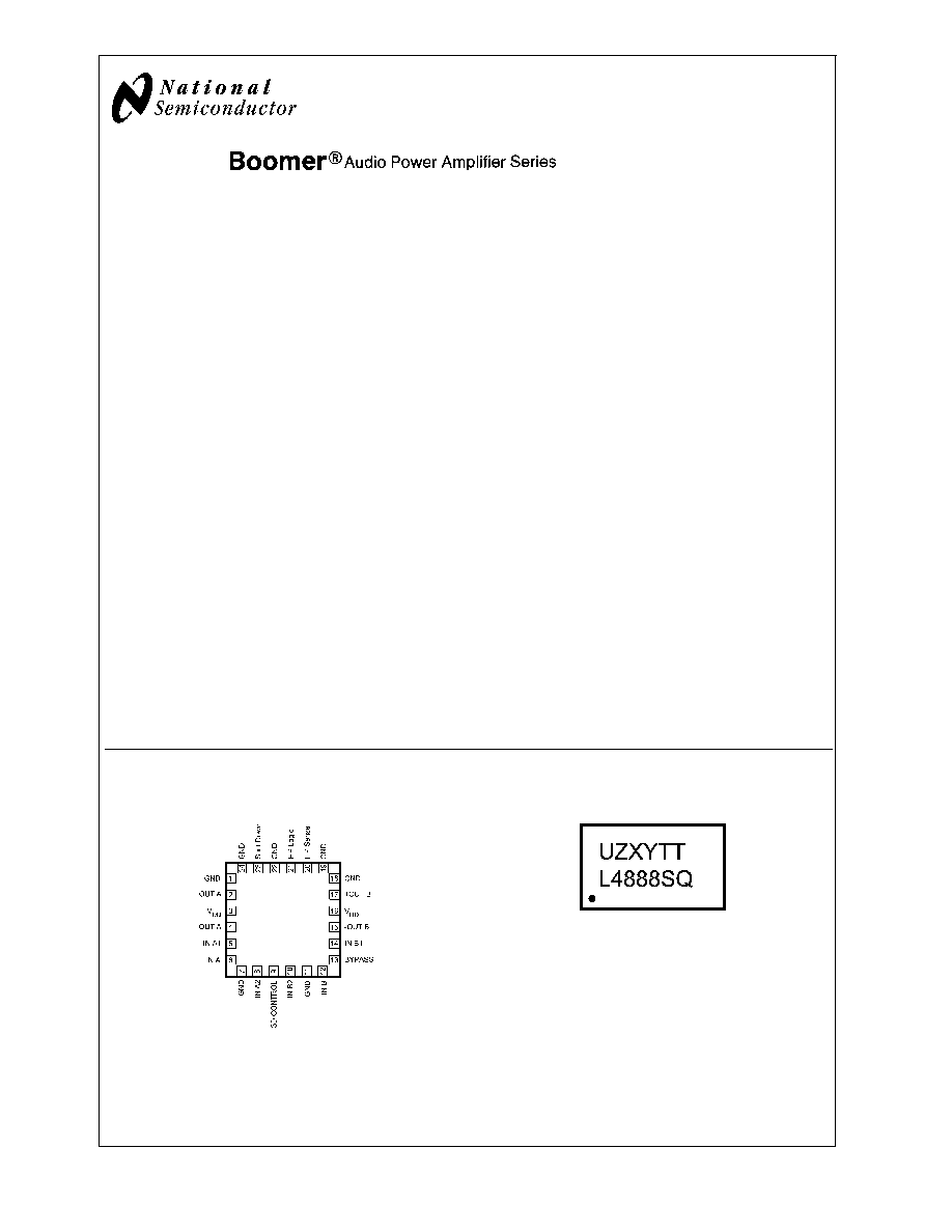
Connection Diagrams
LM4888SQ
LM4888SQ Top Mark
20111602
Top View
Order Number LM4888SQ
See NS Package Number SQA24A
201116C6
Top View
U = Fab Code
Z = Assembly Plant Code
XY = Date Code
TT = Die Traceability
Boomer
®
is a registered trademark of National Semiconductor Corporation.
June 2005
LM4888
Dual
2.1W
Audio
Amplifier
Plus
Stereo
Headphone
&
3
D
Enhancement
© 2005 National Semiconductor Corporation
DS201116
www.national.com
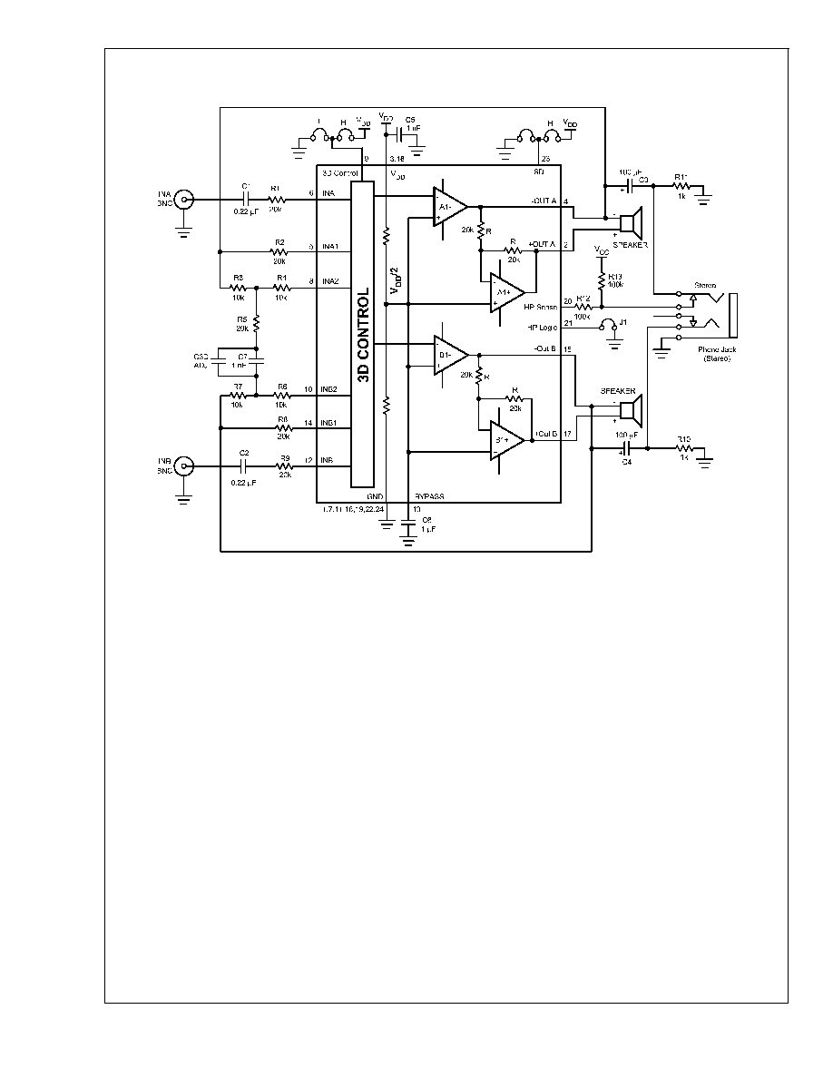
Typical Application
20111601
FIGURE 1. Typical Audio Amplifier Application Circuit
LM4888
www.national.com
2
Absolute Maximum Ratings
(Note 3)
If Military/Aerospace specified devices are required,
please contact the National Semiconductor Sales Office/
Distributors for availability and specifications.
Supply Voltage
6.0V
Storage Temperature
-65°C to +150°C
Input Voltage
-0.3V to V
DD
+0.3V
Power Dissipation (Note 4)
Internally limited
ESD Susceptibility (Note 5)
2000V
ESD Susceptibility (Note 6)
200V
Junction Temperature
150°C
Solder Information
Small Outline Package
Vapor Phase (60 sec.)
215°C
Infrared (15 sec.)
220°C
Thermal Resistance
JC
(typ) -- SQA24B
3°C/W
JA
(typ) -- SQA24B
42°C/W
Operating Ratings
Temperature Range
T
MIN
T
A
T
MAX
-40°C
T
A
85°C
Supply Voltage
2.7V
V
DD
5.5V
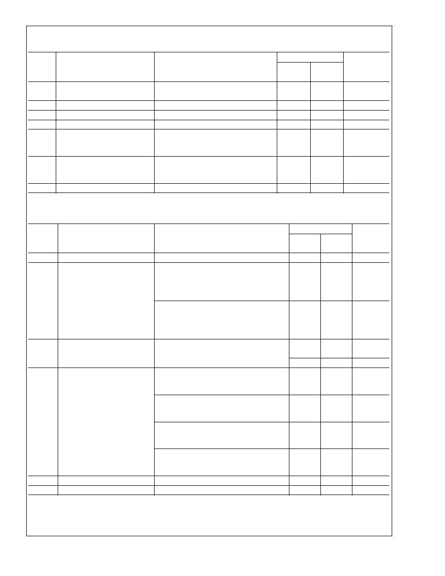
Electrical Characteristics (5V)
(Notes 3, 7, 13)
The following specifications apply for V
DD
= 5V unless otherwise noted. Limits apply for T
A
= 25°C.
Symbol
Parameter
Conditions
LM4888
Units
(Limits)
Typical
Limit
(Note 8)
(Note 9)
V
DD
Supply Voltage
2.7
V (min)
5.5
V (max)
I
DD
Quiescent Power Supply Current
V
IN
= 0V, I
O
= 0A (Note 10) , BTL mode
6
10
mA (max)
V
IN
= 0V, I
O
= 0A (Note 10) , SE mode
3.0
6
mA (max)
I
SD
Shutdown Current
GND applied to the SHUTDOWN pin
0.04
2
µA (max)
V
IH
Headphone Sense High Input
Voltage
3.7
4
V (min)
V
IL
Headphone Sense Low Input
Voltage
2.6
0.8
V (max)
V
IHSD
Shutdown, Headphone micro,
3D control
High Input voltage
1.2
1.4
V (min)
V
ILSD
Shutdown, Headphone micro,
3D control
Low Input voltage
1
0.4
V (max)
T
WU
Turn On Time
1µF Bypass Cap (C6)
140
ms
Electrical Characteristics for Bridged-Mode Operation (5V)
(Notes 3, 7, 13)
The following specifications apply for V
DD
= 5V unless otherwise specified. Limits apply for T
A
= 25°C.
Symbol
Parameter
Conditions
LM4888
Units
(Limits)
Typical
Limit
(Note 8)
(Note 9)
V
OS
Output Offset Voltage
V
IN
= 0V
5
25
mV (max)
P
O
Output Power (Note 11)
THD+N = 1%, f = 1kHz (Note 12)
LM4888SQ, R
L
= 3
2.4
W
LM4888SQ, R
L
= 4
2.1
W
LM4888SQ, R
L
= 8
1.3
1.0
W (min)
THD+N = 10%, f = 1kHz (Note 12)
LM4888SQ, R
L
= 3
3.0
W
LM4888SQ, R
L
= 4
2.5
W
LM4888SQ, R
L
= 8
1.7
W
LM4888
www.national.com
3
Electrical Characteristics for Bridged-Mode Operation (5V)
(Notes 3, 7,
13) (Continued)
The following specifications apply for V
DD
= 5V unless otherwise specified. Limits apply for T
A
= 25°C.
Symbol
Parameter
Conditions
LM4888
Units
(Limits)
Typical
Limit
(Note 8)
(Note 9)
THD+N
Total Harmonic Distortion+Noise
1kHz, A
VD
= 2
LM4888SQ, R
L
= 4
, P
O
= 1W
0.10
%
LM4888SQ, R
L
= 8
, P
O
= .4W
0.06
%
PSRR
Power Supply Rejection Ratio
Input Unterminated, 217Hz
V
ripple
= 200mV
p-p
C
6
= 1µF, R
L
= 8
85
dB
Input Unterminated, 1kHz
V
ripple
= 200mV
p-p
C
6
= 1µF, R
L
= 8
80
dB
Input grounded, 217Hz
V
ripple
= 200mV
p-p
C
6
= 1µF, R
L
= 8
65
dB
Input grounded, 1kHz
V
ripple
= 200mV
p-p
C
6
= 1µF, R
L
= 8
70
dB
X
TALK
Channel Separation
f = 1kHz, C
6
= 1.0µF, 3D Control = Low
82
dB
V
NO
Output Noise Voltage
1kHz, A-weighted
21
µV
Electrical Characteristics for Single-Ended Operation (5V)
(Notes 3, 7, 13)
The following specifications apply for V
DD
= 5V unless otherwise specified. Limits apply for T
A
= 25°C.
Symbol
Parameter
Conditions
LM4888
Units
(Limits)
Typical
Limit
(Note 8)
(Note 9)
P
O
Output Power
THD+N = 0.5%, f = 1 kHz, R
L
= 32
90
75
mW (min)
THD+N
Total Harmonic Distortion+Noise
P
O
= 20mW, 1kHz, R
L
= 32
0.015
%
PSRR
Power Supply Rejection Ratio
Input Unterminated, 217Hz
V
ripple
= 200mV
p-p
C
6
= 1µF, R
L
= 32
70
dB
Input Unterminated, 1kHz
V
ripple
= 200mV
p-p
C
6
= 1µF, R
L
= 32
72
dB
Input grounded, 217Hz
V
ripple
= 200mV
p-p
C
6
= 1µF, R
L
= 32
65
dB
Input grounded, 1kHz
V
ripple
= 200mV
p-p
C
6
= 1µF, R
L
= 32
70
dB
X
TALK
Channel Separation
f = 1kHz, C
6
= 1.0µF, 3D Control = Low
80
dB
V
NO
Output Noise Voltage
1kHz, A-weighted
11
µV
LM4888
www.national.com
4
Electrical Characteristics (3V)
(Notes 3, 7, 13)
The following specifications apply for V
DD
= 3V unless otherwise noted. Limits apply for T
A
= 25°C.
Symbol
Parameter
Conditions
LM4888
Units
(Limits)
Typical
Limit
(Note 8)
(Note 9)
I
DD
Quiescent Power Supply Current
V
IN
= 0V, I
O
= 0A (Note 10) , BTL mode
4.5
mA
V
IN
= 0V, I
O
= 0A (Note 10) , SE mode
2.5
mA
I
SD
Shutdown Current
GND applied to the SHUTDOWN pin
0.01
µA
V
IH
Headphone High Input Voltage
2.2
V
V
IL
Headphone Low Input Voltage
1.5
V
V
IHSD
Shutdown, Headphone micro,
3D Control
High Input voltage
1
1.4
V (min)
V
ILSD
Shutdown, Headphone micro,
3D Control
Low Input voltage
0.8
.4
V (max)
T
WU
Turn On Time
1µF Bypass Cap (C6)
140
ms
Electrical Characteristics for Bridged-Mode Operation (3V)
(Notes 3, 7, 13)
The following specifications apply for V
DD
= 3V unless otherwise specified. Limits apply for T
A
= 25°C.
Symbol
Parameter
Conditions
LM4888
Units
(Limits)
Typical
Limit
(Note 8)
(Note 9)
V
OS
Output Offset Voltage
V
IN
= 0V
5
mV
P
O
Output Power (Note 11)
THD+N = 1%, f = 1kHz (Note 12)
LM4888SQ, R
L
= 3
.82
W
LM4888SQ, R
L
= 4
.70
W
LM4888SQ, R
L
= 8
.43
W
THD+N = 10%, f = 1kHz (Note 12)
LM4888SQ, R
L
= 3
1.0
W
LM4888SQ, R
L
= 4
.85
W
LM4888SQ, R
L
= 8
.53
W
THD+N
Total Harmonic Distortion+Noise
1kHz
LM4888SQ, R
L
= 4
, P
O
= 280mW
0.1
%
LM4888SQ, R
L
= 8
, P
O
= 200mW
0.05
%
PSRR
Power Supply Rejection Ratio
Input Unterminated, 217Hz
V
ripple
= 200mV
p-p
C
6
= 1µF, R
L
= 8
90
dB
Input Unterminated, 1kHz
V
ripple
= 200mV
p-p
C
6
= 1µF, R
L
= 8
80
dB
Input grounded, 217Hz
V
ripple
= 200mV
p-p
C
6
= 1µF, R
L
= 8
65
dB
Input grounded, 1kHz
V
ripple
= 200mV
p-p
C
6
= 1µF, R
L
= 8
73
dB
X
TALK
Channel Separation
f = 1kHz, C
6
= 1.0µF, 3D Control = Low
85
dB
V
NO
Output Noise Voltage
1kHz, A-weighted
21
µV
LM4888
www.national.com
5
Document Outline
- LM4888 Boomer (R) Audio Power Amplifier Series
- General Description
- Key Specifications
- Features
- Applications
- Connection Diagrams
- Typical Application
- Absolute Maximum Ratings
- Operating Ratings
- Electrical Characteristics (5V) (Notes , , )
- Electrical Characteristics for Bridged-Mode Operation (5V) (Notes , , )
- Electrical Characteristics for Single-Ended Operation (5V) (Notes , , )
- Electrical Characteristics (3V) (Notes , , )
- Electrical Characteristics for Bridged-Mode Operation (3V) (Notes , , )
- Electrical Characteristics for Single-Ended Operation (3V) (Notes , , )
- Typical Performance Characteristics
- Application Information
- Demonstration Board Layout
- Bill of Materials
- Revision History
- Physical Dimensions