LM4889
1 Watt Audio Power Amplifier
General Description
The LM4889 is an audio power amplifier primarily designed
for demanding applications in mobile phones and other por-
table communication device applications. It is capable of
delivering 1 watt of continuous average power to an 8
BTL
load with less than 2% distortion (THD+N) from a 5V
DC
power supply.
Boomer audio power amplifiers were designed specifically to
provide high quality output power with a minimal amount of
external components. The LM4889 does not require output
coupling capacitors or bootstrap capacitors, and therefore is
ideally suited for mobile phone and other low voltage appli-
cations where minimal power consumption is a primary re-
quirement.
The LM4889 features a low-power consumption shutdown
mode, which is achieved by driving the shutdown pin with a
logic low. Additionally, the LM4889 features an internal ther-
mal shutdown protection mechanism.
The LM4889 contains advanced pop & click circuitry to
eliminate noise which would otherwise occur during turn-on
and turn-off transitions.
The LM4889 is unity-gain stable and can be configured by
external gain-setting resistors.
Key Specifications
j
Improved PSRR at 217Hz, 5 - 3.3V
75dB
j
Power Output at 5.0V & 2% THD
1.0W(typ.)
j
Power Output at 3.3V & 1% THD
400mW(typ.)
j
Shutdown Current at 3.3 & 2.6V
0.01�A(typ.)
Features
n
Available in space-saving MSOP, SOIC, LLP, and micro
SMD packages
n
Ultra low current shutdown mode (3.3 to 2.6V - 0.01�A)
n
Can drive capacitive loads up to 500 pF
n
Improved pop & click circuitry eliminates noises during
turn-on and turn-off transitions
n
2.2 - 5.5V operation
n
No output coupling capacitors, snubber networks or
bootstrap capacitors required
n
Unity-gain stable
n
External gain configuration capability
Applications
n
Mobile Phones
n
PDAs
n
Portable electronic devices
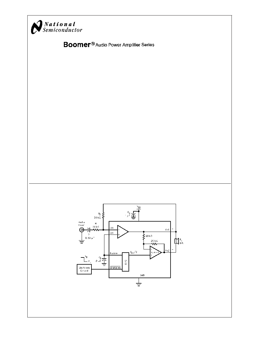
Typical Application
Boomer
�
is a registered trademark of National Semiconductor Corporation.
20035801
FIGURE 1. Typical Audio Amplifier Application Circuit
June 2003
LM4889
1
W
att
Audio
Power
Amplifier
� 2003 National Semiconductor Corporation
DS200358
www.national.com
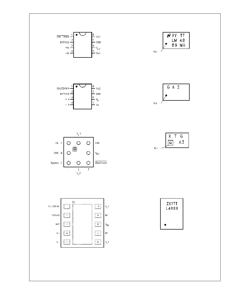
Connection Diagrams
Small Outline (SO) Package
SO Marking
20035835
Top View
Order Number LM4889MA
See NS Package Number M08A
20035872
Top View
XY - Date Code
TT - Die Traceability
Bottom 2 lines - Part Number
Mini Small Outline (MSOP) Package
MSOP Marking
20035836
Top View
Order Number LM4889MM
See NS Package Number MUA08A
20035871
Top View
G - Boomer Family
A2 - LM4889MM
8 Bump micro SMD
8 Bump micro SMD Marking
20035887
Top View
Order Number LM4889ITL, LM4889ITLX
See NS Package Number TLA08AAA
20035879
Top View
X - Date Code
T - Die Traceability
G - Boomer Family
A3 - LM4889ITL
LLP Package
10 Pin LLP Marking
20035830
Top View
Order Number LM4889LD
See NS Package Number LDA10B
20035831
Top View
Z - Assembly Plant Date Code (M for Malacca)
XY - 2 Digit Date Code
TT - Die Traceability
L4889 - LM4889LD
LM4889
www.national.com
2
Absolute Maximum Ratings
(Note 2)
If Military/Aerospace specified devices are required,
please contact the National Semiconductor Sales Office/
Distributors for availability and specifications.
Supply Voltage
6.0V
Storage Temperature
-65�C to +150�C
Input Voltage
-0.3V to V
DD
+0.3V
Power Dissipation (Note 3)
Internally Limited
ESD Susceptibility (Note 4)
2000V
ESD Susceptibility (Note 5)
200V
Junction Temperature
150�C
Thermal Resistance
JC
(SOP)
35�C/W
JA
(SOP)
150�C/W
JA
(8 Bump micro SMD) (Note 10)
210�C/W
JC
(MSOP)
56�C/W
JA
(MSOP)
190�C/W
JA
(LLP)
220�C/W
Soldering Information
See AN-1112 "microSMD Wafers Level Chip Scale
Package".
Operating Ratings
Temperature Range
T
MIN
T
A
T
MAX
-40�C
T
A
85�C
Supply Voltage
2.2V
V
DD
5.5V
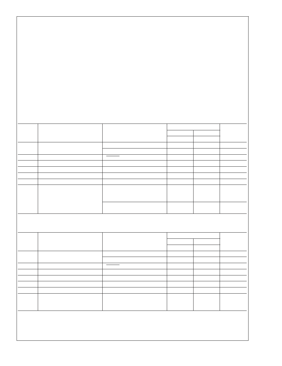
Electrical Characteristics V
DD
= 5V
(Notes 1, 2)
The following specifications apply for V
DD
= 5V, A
V
= 2, and 8
load unless otherwise specified. Limits apply for T
A
= 25�C.
Symbol
Parameter
Conditions
LM4889
Units
(Limits)
Typical
Limit
(Note 6)
(Notes 7, 9)
I
DD
Quiescent Power Supply Current
V
IN
= 0V, I
o
= 0A, no Load
4
8
mA (max)
V
IN
= 0V, I
o
= 0A, with BTL Load
5
8
mA (max)
I
SD
Shutdown Current
V
shutdown
= GND (Note 8)
0.1
1
�A (max)
V
SDIH
Shutdown Voltage Input High
1.2
V (min)
V
SDIL
Shutdown Voltage Input Low
0.4
V (max)
P
o
Output Power
THD = 2% (max); f = 1 kHz
1
W
THD+N
Total Harmonic Distortion+Noise
P
o
= 0.4 Wrms; f = 1kHz
0.1
%
PSRR
Power Supply Rejection Ratio
V
ripple
= 200mV sine p-p
f
ripple
= 217Hz
f
ripple
= 1kHz
62
66
dB
dB
V
ripple
= 200mV sine p-p
Input Floating
75
68
dB
Electrical Characteristics V
DD
= 3.3V
(Notes 1, 2)
The following specifications apply for V
DD
= 3.3V, A
V
= 2, and 8
load unless otherwise specified. Limits apply for T
A
= 25�C.
Symbol
Parameter
Conditions
LM4889
Units
(Limits)
Typical
Limit
(Note 6)
(Notes 7, 9)
I
DD
Quiescent Power Supply Current
V
IN
= 0V, I
o
= 0A, no Load
3.5
7
mA (max)
V
IN
= 0V, I
o
= 0A, with BTL Load
4.5
7
mA (max)
I
SD
Shutdown Current
V
shutdown
= GND (Note 8)
0.01
1
�A (max)
V
SDIH
Shutdown Voltage Input High
1.2
V (min)
V
SDIL
Shutdown Voltage Input Low
0.4
V (max)
P
o
Output Power
THD = 1% (max); f = 1kHz
0.4
W
THD+N
Total Harmonic Distortion+Noise
P
o
= 0.25Wrms; f = 1kHz
0.1
%
PSRR
Power Supply Rejection Ratio
V
ripple
= 200mV sine p-p
f
ripple
= 217Hz
f
ripple
=1kHz
60
62
dB
dB
LM4889
www.national.com
3
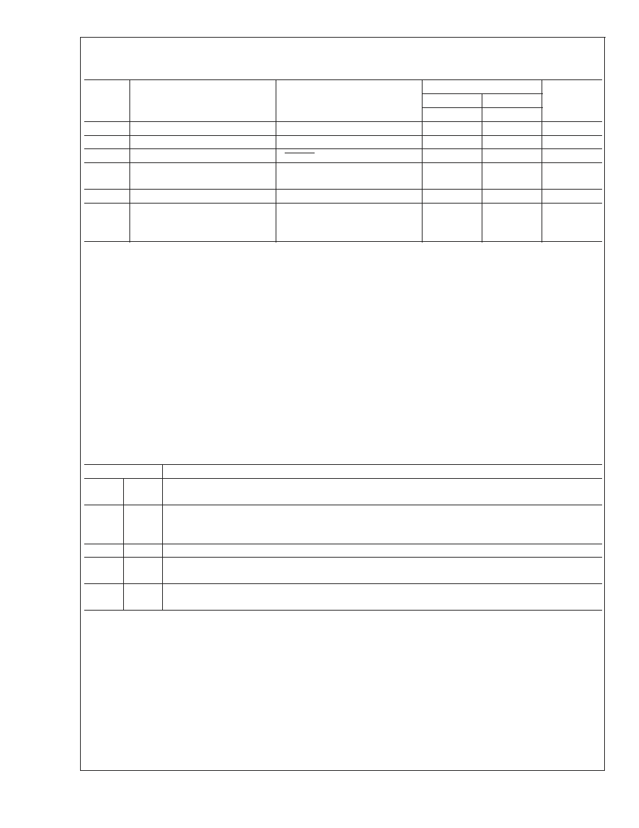
Electrical Characteristics V
DD
= 2.6V
(Notes 1, 2)
The following specifications apply for V
DD
= 2.6V, A
V
= 2, and 8
load unless otherwise specified. Limits apply for T
A
= 25�C.
Symbol
Parameter
Conditions
LM4889
Units
(Limits)
Typical
Limit
(Note 6)
(Notes 7, 9)
I
DD
Quiescent Power Supply Current
V
IN
= 0V, I
o
= 0A, no Load
2.6
6
mA (max)
V
IN
= 0V, I
o
= 0A, with BTL Load
3.0
6
mA (max)
I
SD
Shutdown Current
V
shutdown
= GND (Note 8)
0.01
1
�A (max)
P
0
Output Power ( 8
)
Output Power ( 4
)
THD = 1% (max); f = 1 kHz
THD = 1% (max); f = 1 kHz
0.2
0.22
W
W
THD+N
Total Harmonic Distortion+Noise
P
o
= 0.1Wrms; f = 1kHz
0.08
%
PSRR
Power Supply Rejection Ratio
V
ripple
= 200mV sine p-p
f
ripple
= 217Hz
f
ripple
= 1kHz
44
44
dB
dB
Note 1: All voltages are measured with respect to the ground pin, unless otherwise specified.
Note 2: Absolute Maximum Ratings indicate limits beyond which damage to the device may occur. Operating Ratings indicate conditions for which the device is
functional, but do not guarantee specific performance limits. Electrical Characteristics state DC and AC electrical specifications under particular test conditions which
guarantee specific performance limits. This assumes that the device is within the Operating Ratings. Specifications are not guaranteed for parameters where no limit
is given, however, the typical value is a good indication of device performance.
Note 3: The maximum power dissipation must be derated at elevated temperatures and is dictated by T
JMAX
,
JA
, and the ambient temperature T
A
. The maximum
allowable power dissipation is P
DMAX
= (T
JMAX
�T
A
)/
JA
or the number given in Absolute Maximum Ratings, whichever is lower. For the LM4889, see power derating
currents for additional information.
Note 4: Human body model, 100 pF discharged through a 1.5 k
resistor.
Note 5: Machine Model, 220 pF�240 pF discharged through all pins.
Note 6: Typicals are measured at 25�C and represent the parametric norm.
Note 7: Limits are guaranteed to National's AOQL (Average Outgoing Quality Level).
Note 8: For micro SMD only, shutdown current is measured in a Normal Room Environment. Exposure to direct sunlight will increase I
SD
by a maximum of 2�A.
Note 9: Datasheet min/max specification limits are guaranteed by design, test or statistical analysis.
Note 10: All bumps have the same thermal resistance and contribute equally when used to lower thermal resistance. The LM4889ITL demo board (views featured
in the Application Information section) has two inner layers, one for V
DD
and one for GND. The planes each measure 600mils x 600mils (15.24mm x 15.24mm)
and aid in spreading heat due to power dissipation within the IC.
External Components Description
(Figure 1)
Components
Functional Description
1.
R
i
Inverting input resistance which sets the closed-loop gain in conjunction with R
f
. This resistor also forms a
high pass filter with C
i
at f
C
= 1/(2
R
i
C
i
).
2.
C
i
Input coupling capacitor which blocks the DC voltage at the amplifiers input terminals. Also creates a
highpass filter with R
i
at f
c
= 1/(2
R
i
C
i
). Refer to the section, Proper Selection of External Components,
for an explanation of how to determine the value of C
i
.
3.
R
f
Feedback resistance which sets the closed-loop gain in conjunction with R
i
. A
VD
= 2
*
(R
f
/R
i
).
4.
C
S
Supply bypass capacitor which provides power supply filtering. Refer to the Power Supply Bypassing
section for information concerning proper placement and selection of the supply bypass capacitor.
5.
C
B
Bypass pin capacitor which provides half-supply filtering. Refer to the section, Proper Selection of External
Components, for information concerning proper placement and selection of C
B
.
LM4889
www.national.com
4
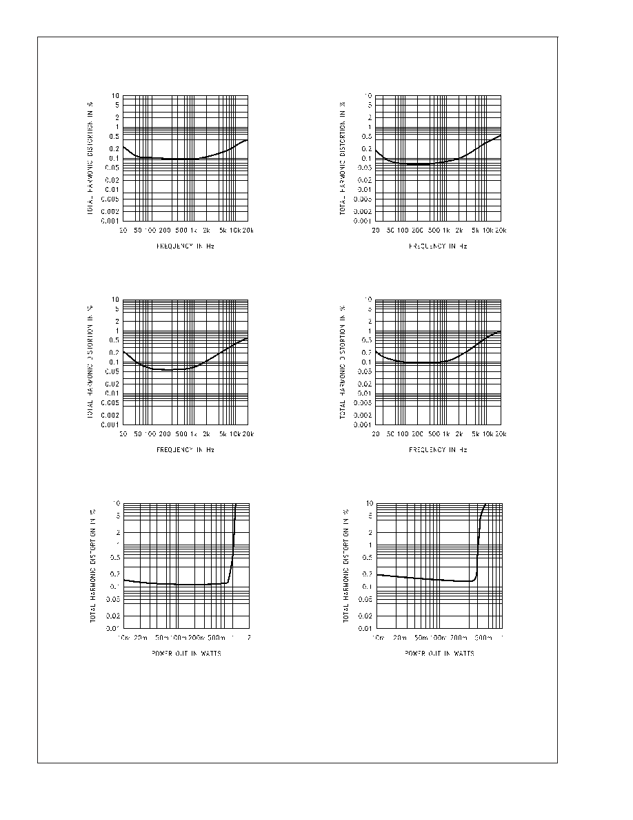
Typical Performance Characteristics
THD+N vs Frequency
at V
DD
= 5V, 8
R
L
, and PWR = 250mW
THD+N vs Frequency
at V
DD
= 3.3V, 8
R
L
, and PWR = 150mW
20035837
20035838
THD+N vs Frequency
at V
DD
= 2.6V, 8
R
L
, and PWR = 100mW
THD+N vs Frequency
at V
DD
= 2.6V, 4
R
L
, and PWR = 100mW
20035839
20035840
THD+N vs Power Out
at V
DD
= 5V, 8
R
L
, 1kHz
THD+N vs Power Out
at V
DD
= 3.3V, 8
R
L
, 1kHz
20035875
20035842
LM4889
www.national.com
5