 | ÐлекÑÑоннÑй компоненÑ: LM4897 | СкаÑаÑÑ:  PDF PDF  ZIP ZIP |
Äîêóìåíòàöèÿ è îïèñàíèÿ www.docs.chipfind.ru
LM4897
1.1 Watt Audio Power Amplifier with Fade-In and
Fade-Out
General Description
The LM4897 is an audio power amplifier primarily designed
for demanding applications in mobile phones and other por-
table communication device applications. It is capable of
delivering 1.1W of continuous average power to an 8
BTL
load with less than 1% distortion (THD+N) from a +5V
DC
power supply.
The LM4897 contains advanced pop and click circuitry that
eliminate noises which would otherwise occur during turn-on
and turn-off transitions. It also contains a fade-in/fade-out
feature that eliminates unnatural sound generated by
asserting/de-asserting the SHUTDOWN pin. The LM4897 is
unity-gain stable and can be configured by external gain-
setting resistors.
The LM4897 features a low-power consumption global shut-
down mode, which is achieved by driving the shutdown pin
with logic low. Additionally, the LM4897 features an internal
thermal shutdown protection mechanism.
Boomer audio power amplifiers were designed specifically to
provide high quality output power with a minimal amount of
external components. The LM4897 does not require output
coupling capacitors or bootstrap capacitors, and therefore is
ideally suited for lower-power portable applications where
minimal space and power consumption are primary require-
ments.
Key Specifications
j
Improved PSRR at 5V, 3V, & 217Hz
62dB (typ)
j
Higher P
O
at 5V, THD+N = 1%
1.1W (typ)
j
Higher P
O
at 3V, THD+N = 1%
350mW (typ)
j
Shutdown Current
0.1µA (typ)
Features
n
No output coupling capacitors, snubber networks or
bootstrap capacitors required
n
Unity gain stable
n
Ultra low current shutdown mode
n
Fade-In/Fade-Out
n
BTL output can drive capacitive loads up to 100pF
n
Advanced pop and click circuitry eliminates noises
during turn-on and turn-off transitions
n
2.6V - 5.5V operation
n
Available in a space-saving SO package
Applications
n
Mobile Phones
n
PDAs
n
Portable electronic devices
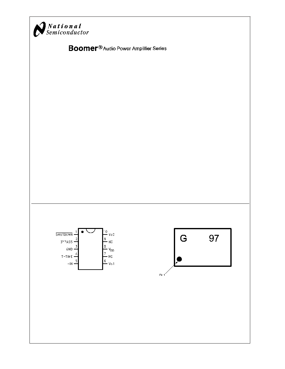
Connection Diagrams
Mini Small Outline (MSOP) Package
MSOP Marking
20050930
Top View
Order Number LM4897MM
See NS package Number MUB10A
200509D0
Top View
G - Boomer Family
97 - LM4897MM
Boomer
®
is a registered trademark of National Semiconductor Corporation.
May 2003
LM4897
1.1
W
att
Audio
Power
Amplifier
with
Fade-In
and
Fade-Out
© 2003 National Semiconductor Corporation
DS200509
www.national.com
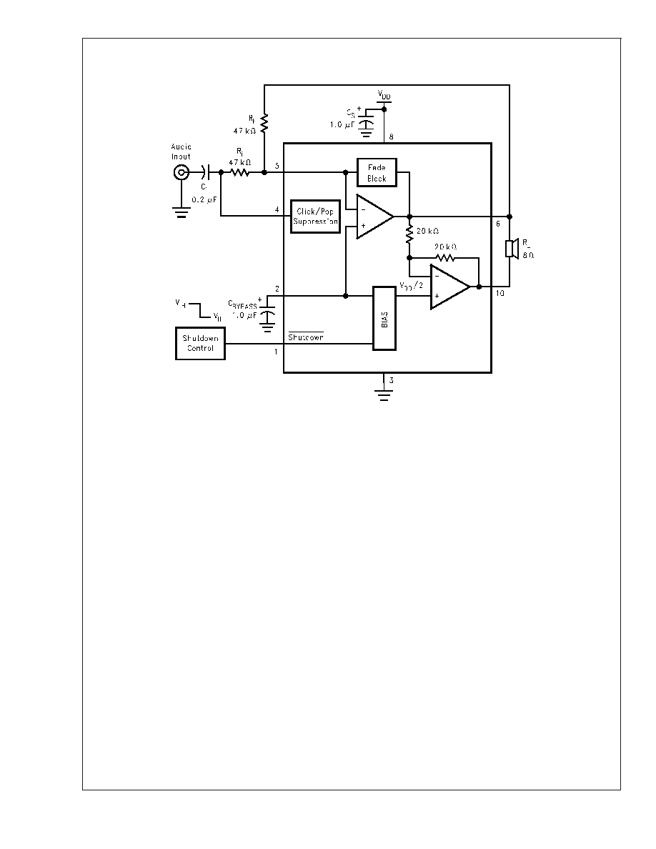
Typical Application
20050901
FIGURE 1. Typical Audio Amplifier Application Circuit
LM4897
www.national.com
2
Absolute Maximum Ratings
(Note 2)
If Military/Aerospace specified devices are required,
please contact the National Semiconductor Sales Office/
Distributors for availability and specifications.
Supply Voltage
6.0V
Storage Temperature
-65°C to +150°C
Input Voltage
-0.3V to V
DD
+0.3V
Power Dissipation (Note 3)
Internally Limited
ESD Susceptibility (Note 4)
2000V
ESD Susceptibility (Note 5)
200V
Junction Temperature
150°C
Thermal Resistance
JC
(MUB10A)
56°C/W
JA
(MUB10A)
190°C/W
Operating Ratings
Temperature Range
T
MIN
T
A
T
MAX
-40°C
T
A
85°C
Supply Voltage
2.6V
V
DD
5.5V
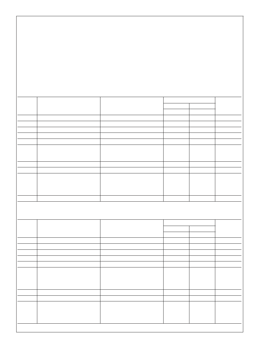
Electrical Characteristics V
DD
= 5.0V
(Notes 1, 2)
The following specifications apply for the circuit shown in Figure 1 unless otherwise specified. Limits apply for T
A
= 25°C.
Symbol
Parameter
Conditions
LM4897
Units
(Limits)
Typical
Limit
(Note 6)
(Notes 7, 8)
I
DD
Quiescent Power Supply Current
V
IN
= 0V, 8
BTL
5
9
mA (max)
I
SD
Shutdown Current
V
shutdown
= GND
0.1
2
µA (max)
V
OS
Output Offset Voltage
4
30
mV (max)
P
o
Output Power
THD+N = 1% (max), f = 1kHz
1.1
0.9
W (min)
THD+N
Total Harmonic Distortion+Noise
P
o
= 0.4Wrms, f = 1kHz
0.1
%
PSRR
Power Supply Rejection Ratio
V
ripple
= 200mVpp sine wave,
C
B
= 1.0µF
Input terminated with 10
to GND
63 (f = 1kHz)
62 (f =
217Hz)
55
55
dB (min)
V
SDIH
Shutdown High Input Voltage
1.4
V (min)
V
SDIL
Shutdown Low Input Voltage
0.4
V (max)
V
ON
Output Noise
A-Weighted, Measured across 8
BTL
Input terminated with 10
to
ground
26
µV
RMS
T
ON
Turn-On Time
C
BYPASS
= 1µF
25
35
ms (max)
Electrical Characteristics V
DD
= 3.0V
(Notes 1, 2)
The following specifications apply for the circuit shown in Figure 1 unless otherwise specified. Limits apply for T
A
= 25°C.
Symbol
Parameter
Conditions
LM4897
Units
(Limits)
Typical
Limit
(Note 6)
(Notes 7, 8)
I
DD
Quiescent Power Supply Current
V
IN
= 0V, 8
BTL
4
8
mA (max)
I
SD
Shutdown Current
V
shutdown
= GND
0.1
2
µA (max)
P
o
Output Power
THD+N = 1% (max), f = 1kHz
350
320
mW (min)
V
OS
Output Offset Voltage
4
30
mV (max)
THD+N
Total Harmonic Distortion+Noise
P
o
= 0.15Wrms, f = 1kHz
0.1
%
PSRR
Power Supply Rejection Ratio
V
ripple
= 200mVpp sine wave,
C
B
= 1.0µF
Input terminated with 10
to
ground
63 (f = 1kHz)
62 (f =
217Hz)
55
55
dB (min)
V
SDIH
Shutdown High Input Voltage
1.4
V (min)
V
SDIL
Shutdown Low Input Voltage
0.4
V (max)
V
ON
Output Voltage Noise
A-Weighted, Measured across 8
BTL
Input terminated with 10
to
ground
26
µV
RMS
LM4897
www.national.com
3
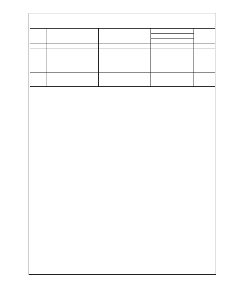
Electrical Characteristics V
DD
= 2.6V
(Notes 1, 2)
The following specifications apply for the circuit shown in Figure 1 unless otherwise specified. Limits apply for T
A
= 25°C.
Symbol
Parameter
Conditions
LM4897
Units
(Limits)
Typical
Limit
(Note 6)
(Notes 7, 8)
I
DD
Quiescent Power Supply Current
V
IN
= 0V, 8
BTL
3.5
7
mA (max)
I
SD
Shutdown Current
V
shutdown
= GND
0.1
2
µA (max)
V
OS
Output Offset Voltage
4
30
mV (max)
P
o
Output Power
THD+N = 1% (max), f = 1kHz
mW (min)
R
L
= 8
250
THD+N
Total Harmonic Distortion+Noise
P
o
= 0.1Wrms, f = 1kHz
0.1
%
PSRR
Power Supply Rejection Ratio
V
ripple
= 200mVpp sine wave,
C
B
= 1.0µF
Input terminated with 10
to GND
55 (f = 1kHz)
55 (f =
217Hz)
dB
Note 1: All voltages are measured with respect to the ground pin, unless otherwise specified.
Note 2: Absolute Maximum Ratings indicate limits beyond which damage to the device may occur. Operating Ratings indicate conditions for which the device is
functional, but do not guarantee specific performance limits. Electrical Characteristics state DC and AC electrical specifications under particular test conditions which
guarantee specific performance limits. This assumes that the device is within the Operating Ratings. Specifications are not guaranteed for parameters where no limit
is given, however, the typical value is a good indication of device performance.
Note 3: The maximum power dissipation must be derated at elevated temperatures and is dictated by T
JMAX
,
JA
, and the ambient temperature T
A
. The maximum
allowable power dissipation is P
DMAX
= (T
JMAX
T
A
)/
JA
or the number given in Absolute Maximum Ratings, whichever is lower. For the LM4897, see power derating
curves for additional information.
Note 4: Human body model, 100pF discharged through a 1.5k
resistor.
Note 5: Machine Model, 220pF240pF discharged through all pins.
Note 6: Typicals are measured at 25°C and represent the parametric norm.
Note 7: Limits are guaranteed to National's AOQL (Average Outgoing Quality Level).
Note 8: Exposure to direct sunlight will increase I
SD
by a maximum of 2µA.
Note 9: If the product is in shutdown mode, and V
DD
exceeds 6V (to a max of 8V V
DD
), then most of the excess current will flow through the ESD protection circuits.
If the source impedance limits the current to a max of 10ma, then the part will be protected. If the part is enabled when V
DD
is above 6V, circuit performance will
be curtailed or the part may be permanently damaged.
Note 10: All bumps have the same thermal resistance and contribute equally when used to lower thermal resistance.
Note 11: Maximum power dissipation (P
DMAX
) in the device occurs at an output power level significantly below full output power. P
DMAX
can be calculated using
Equation 1 shown in the Application section. It may also be obtained from the power dissipation graphs.
LM4897
www.national.com
4
External Components Description
(Figure 1)
Components
Functional Description
1.
R
i
Inverting input resistance which sets the closed-loop gain in conjunction with R
f
. This resistor also forms a
high pass filter with C
i
at f
C
= 1/(2
R
i
C
i
).
2.
C
i
Input coupling capacitor which blocks the DC voltage at the amplifiers input terminals. Also creates a
highpass filter with R
i
at f
C
= 1/(2
R
i
C
i
). Refer to the section, Proper Selection of External Components, for
an explanation of how to determine the value of C
i
.
3.
R
f
Feedback resistance which sets the closed-loop gain in conjunction with R
i
.
4.
C
S
Supply bypass capacitor which provides power supply filtering. Refer to the Power Supply Bypassing
section for information concerning proper placement and selection of the supply bypass capacitor.
5.
C
B
Bypass pin capacitor which provides half-supply filtering. Refer to the section, Proper Selection of External
Components, for information concerning proper placement and selection of C
B
.
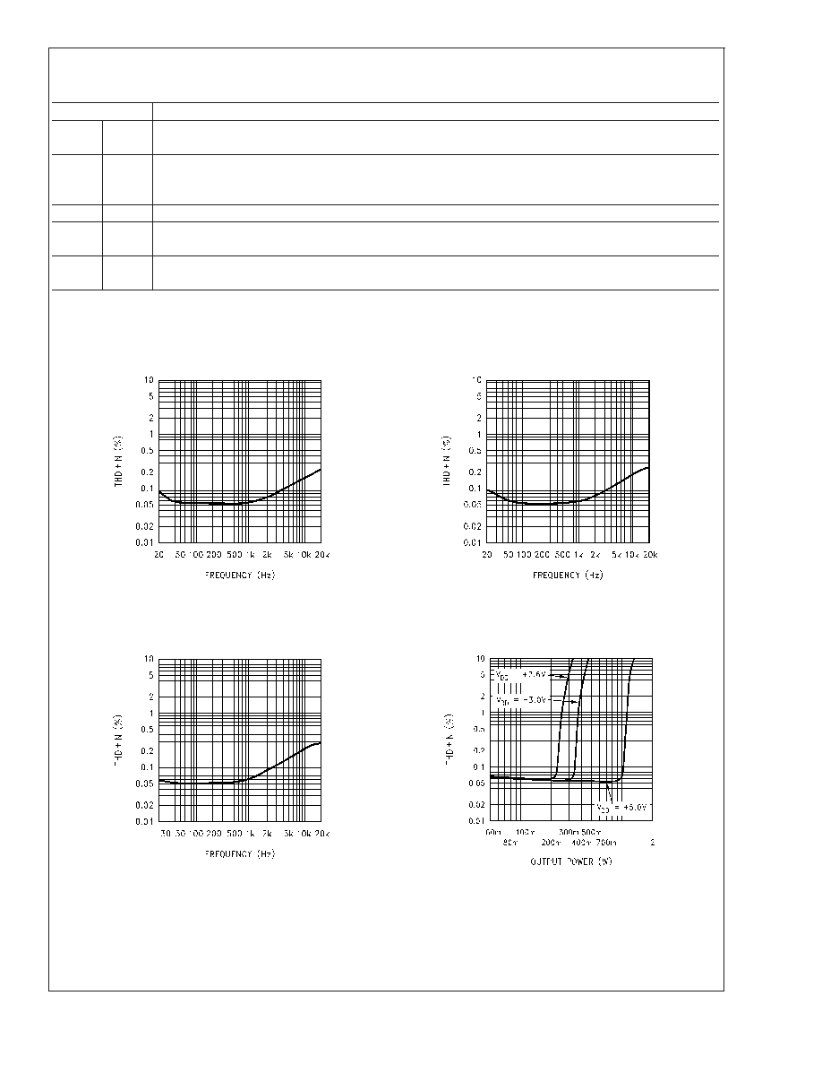
Typical Performance Characteristics
THD+N vs Frequency
V
DD
= 5V, R
L
= 8
PWR = 250mW
THD+N vs Frequency
V
DD
= 3V, R
L
= 8
PWR = 150mW
200509A2
200509A3
THD+N vs Frequency
V
DD
= 2.6V, R
L
= 8
PWR = 100mW
THD+N vs Power Out
V
DD
= 5V
R
L
= 8
, f = 1kHz
200509A4
200509A5
LM4897
www.national.com
5
Document Outline