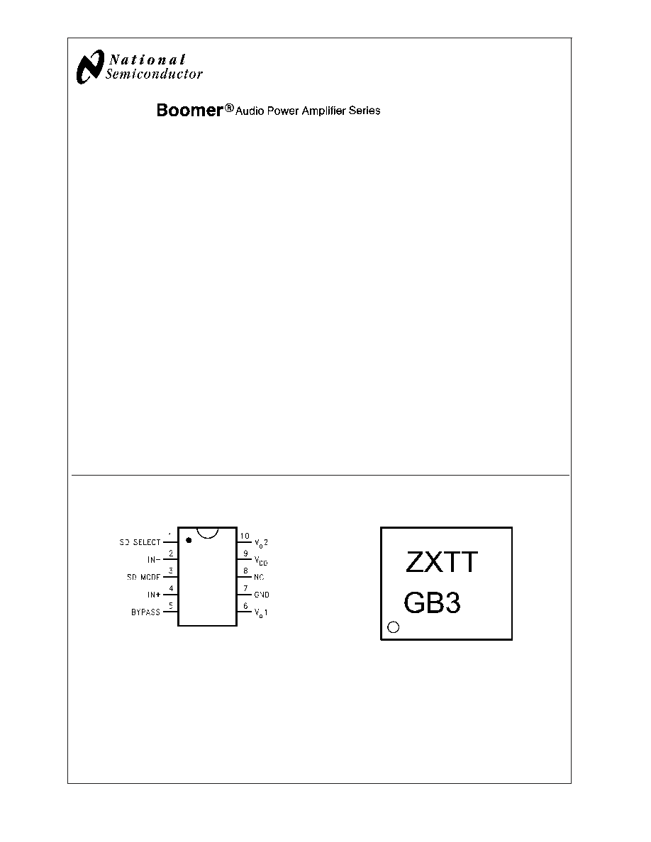
LM4898
1 Watt Fully Differential Audio Power Amplifier With
Shutdown Select
General Description
The LM4898 is a fully differential audio power amplifier
primarily designed for demanding applications in mobile
phones and other portable communication device applica-
tions. It is capable of delivering 1 watt of continuous average
power to an 8
BTL load with less than 1% distortion
(THD+N) from a 5V
DC
power supply.
Boomer audio power amplifiers were designed specifically to
provide high quality output power with a minimal amount of
external components. The LM4898 does not require output
coupling capacitors or bootstrap capacitors, and therefore is
ideally suited for mobile phone and other low voltage appli-
cations where minimal power consumption is a primary re-
quirement.
The LM4898 features a low-power consumption shutdown
mode. To facilitate this, Shutdown may be enabled by either
logic high or low depending on mode selection. Driving the
shutdown mode pin either high or low enables the shutdown
select pin to be driven in a likewise manner to enable Shut-
down. Additionally, the LM4898 features an internal thermal
shutdown protection mechanism.
The LM4898 contains advanced pop & click circuitry which
virtually eliminates noises which would otherwise occur dur-
ing turn-on and turn-off transitions.
Key Specifications
j
Improved PSRR at 217Hz
83dB(typ)
j
Power Output at 5.0V & 1% THD
1.0W(typ)
j
Power Output at 3.3V & 1% THD
400mW(typ)
j
Shutdown Current
0.1µA(typ)
Features
n
Fully differential amplification
n
Available in space-saving packages micro SMD, MSOP,
and LLP
n
Ultra low current shutdown mode
n
Can drive capacitive loads up to 500pF
n
Improved pop & click circuitry eliminates noises during
turn-on and turn-off transitions
n
2.4 - 5.5V operation
n
No output coupling capacitors, snubber networks or
bootstrap capacitors required
n
Shutdown high or low selectivity
Applications
n
Mobile phones
n
PDAs
n
Portable electronic devices
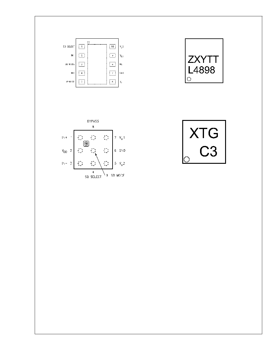
Connection Diagrams
Mini Small Outline (MSOP) Package
MSOP Marking
20073723
Top View
Order Number LM4898MM
See NS Package Number MUB10A
20073774
Z -Assembly Code
X - Date Code
TT - Die Run Traceability
G - Boomer Family
B3 - LM4898MM
Boomer
Æ
is a registered trademark of National Semiconductor Corporation.
July 2003
LM4898
1
W
att
Fully
Differential
Audio
Power
Amplifier
W
ith
Shutdown
Select
© 2003 National Semiconductor Corporation
DS200737
www.national.com
Absolute Maximum Ratings
(Note 2)
If Military/Aerospace specified devices are required,
please contact the National Semiconductor Sales Office/
Distributors for availability and specifications.
Supply Voltage
6.0V
Storage Temperature
-65∞C to +150∞C
Input Voltage
-0.3V to V
DD
+0.3V
Power Dissipation (Note 3)
Internally Limited
ESD Susceptibility (Note 4)
2000V
ESD Susceptibility (Note 5)
200V
Junction Temperature
150∞C
Thermal Resistance
JC
(LLP)
12∞C/W
JA
(LLP)
63∞C/W
JA
(micro SMD)
220∞C/W
JC
(MSOP)
56∞C/W
JA
(MSOP)
190∞C/W
Soldering Information
See AN-1112 "microSMD Wafers Level Chip Scale
Package."
Operating Ratings
Temperature Range
T
MIN
T
A
T
MAX
-40∞C
T
A
85∞C
Supply Voltage
2.4V
V
DD
5.5V
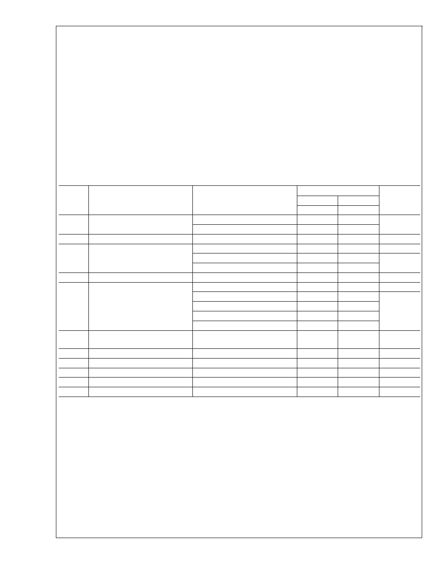
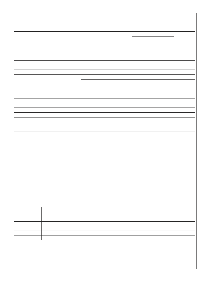
Electrical Characteristics V
DD
= 5V
(Notes 1, 2, 8)
The following specifications apply for V
DD
= 5V,
8
load, and A
V
= 1V/V, unless otherwise specified. Limits apply for T
A
= 25∞C.
Symbol
Parameter
Conditions
LM4898
Units
(Limits)
Typical
Limit
(Note 6)
(Note 7)
I
DD
Quiescent Power Supply Current
V
IN
= 0V, no load
3
6
mA (max)
V
IN
= 0V, R
L
= 8
5
10
I
SD
Shutdown Current
V
SDMODE
= V
SHUTDOWN
= GND
0.1
1
µA (max)
P
o
Output Power
THD = 1% (max); f = 1 kHz
LM4898LD, R
L
= 4
(Note 11)
1.4
W (min)
LM4898, R
L
= 8
1
0.9
THD+N
Total Harmonic Distortion+Noise
P
o
= 0.4 Wrms; f = 1kHz
0.05
%
PSRR
Power Supply Rejection Ratio
V
ripple
= 200mV sine p-p
f = 217Hz (Note 9)
83
dB (min)
f = 1kHz (Note 9)
90
f = 217Hz (Note 10)
83
71
f = 1kHz (Note 10)
83
71
CMRR
Common_Mode Rejection Ratio
f = 217Hz
V
CM
= 200mV
DD
50
dB
V
OS
Output Offset
V
IN
= 0V
2
mV
V
SDIH
Shutdown Voltage Input High
SD Mode = GND
0.9
V
V
SDIL
Shutdown Voltage Input Low
SD Mode = GND
0.7
V
V
SDIH
Shutdown Voltage Input High
SD Mode = V
DD
0.9
V
V
SDIL
Shutdown Voltage Input Low
SD Mode = V
DD
0.7
V
LM4898
www.national.com
4
Electrical Characteristics V
DD
= 3V
(Notes 1, 2, 8)
The following specifications apply for V
DD
= 3V, 8
load and A
V
= 1V/V, unless otherwise specified. Limits apply for T
A
=
25∞C.
Symbol
Parameter
Conditions
LM4898
Units
(Limits)
Typical
Limit
(Note 6)
(Note 7)
I
DD
Quiescent Power Supply Current
V
IN
= 0V, no load
2.5
5 .5
mA (max)
V
IN
= 0V, R
L
= 8
4
9
I
SD
Shutdown Current
V
SDMODE
= V
SHUTDOWN
= GND
0.1
1
µA (max)
P
o
Output Power
THD = 1% (max); f = 1kHz
LM4898, RL = 8
0.35
W
THD+N
Total Harmonic Distortion+Noise
P
o
= 0.25Wrms; f = 1kHz
0.03
%
PSRR
Power Supply Rejection Ratio
V
ripple
= 200mV sine p-p
f = 217Hz (Note 9)
83
dB
f = 1kHz (Note 9)
84
f = 217Hz (Note 10)
83
f = 1kHz (Note 10)
83
CMRR
Common-Mode Rejection Ratio
f = 217Hz
V
CM
= 200mV
PP
50
dB
V
OS
Output Offset
V
IN
= 0V
2
mV
V
SDIH
Shutdown Voltage Input High
SD Mode = GND
0.8
V
V
SDIL
Shutdown Voltage Input Low
SD Mode = GND
0.6
V
V
SDIH
Shutdown Voltage Input High
SD Mode = V
DD
0.8
V
V
SDIL
Shutdown Voltage Input Low
SD Mode = V
DD
0.6
V
Note 1: All voltages are measured with respect to the ground pin, unless otherwise specified.
Note 2: Absolute Maximum Ratings indicate limits beyond which damage to the device may occur. Operating Ratings indicate conditions for which the device is
functional, but do not guarantee specific performance limits. Electrical Characteristics state DC and AC electrical specifications under particular test conditions which
guarantee specific performance limits. This assumes that the device is within the Operating Ratings. Specifications are not guaranteed for parameters where no limit
is given, however, the typical value is a good indication of device performance.
Note 3: The maximum power dissipation must be derated at elevated temperatures and is dictated by T
JMAX
,
JA
, and the ambient temperature T
A
. The maximum
allowable power dissipation is P
DMAX
= (T
JMAX
≠T
A
)/
JA
or the number given in Absolute Maximum Ratings, whichever is lower.
Note 4: Human body model, 100pF discharged through a 1.5k
resistor.
Note 5: Machine Model, 220pF≠240pF discharged through all pins.
Note 6: Typicals are measured at 25∞C and represent the parametric norm.
Note 7: Datasheet min/max specification limits are guaranteed by design, test, or statistical analysis.
Note 8: For micro SMD only, shutdown current is measured in a Normal Room Environment. Exposure to direct sunlight will increase I
SD
by a maximum of 2µA.
Note 9: Unterminated input.
Note 10: 10
terminated input.
Note 11: When driving 4
loads from a 5V supply, the LM4898LD must be mounted to a circuit board with the exposed-DAP area soldered down to a 1sq. in plane
of 1oz. copper..
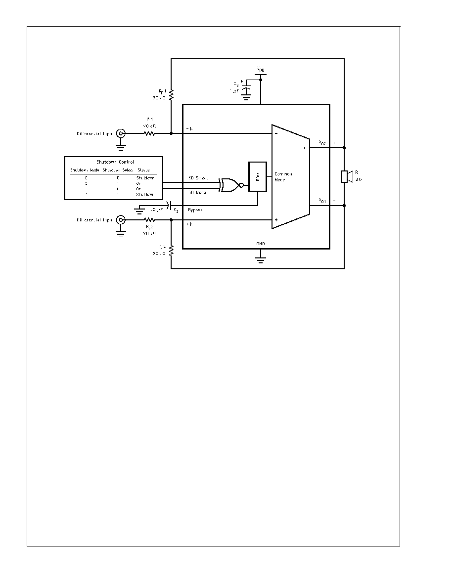
External Components Description
(Figure 1)
Components
Functional Description
1.
C
S
Supply bypass capacitor which provides power supply filtering. Refer to the Power Supply Bypassing
section for information concerning proper placement and selection of the supply bypass capacitor.
2.
C
B
Bypass pin capacitor which provides half-supply filtering. Refer to the section, Proper Selection of External
Components, for information concerning proper placement and selection of C
B
.
3.
R
i
Inverting input resistance which sets the closed-loop gain in conjunction with R
f
.
4.
R
f
Feedback resistance which sets the closed-loop gain in conjunction with R
i
.
LM4898
www.national.com
5