LM4910
Output Capacitor-less Stereo 35mW Headphone
Amplifier
General Description
The LM4910 is an audio power amplifier primarily designed
for headphone applications in portable device applications. It
is capable of delivering 35mW of continuous average power
to a 32
load with less than 1% distortion (THD+N) from a
3.3V
DC
power supply.
The LM4910 utilizes a new circuit topology that eliminates
output coupling capacitors and half-supply bypass capaci-
tors (patent pending). The LM4910 contains advanced pop &
click circuitry which eliminates noises caused by transients
that would otherwise occur during turn-on and turn-off.
Boomer audio power amplifiers were designed specifically to
provide high quality output power with a minimal amount of
external components. Since the LM4910 does not require
any output coupling capacitors, half-supply bypass capaci-
tors, or bootstrap capacitors, it is ideally suited for low-power
portable applications where minimal space and power con-
sumption are primary requirements.
The LM4910 features a low-power consumption shutdown
mode, activated by driving the shutdown pin with logic low.
Additionally, the LM4910 features an internal thermal shut-
down protection mechanism. The LM4910 is also unity-gain
stable and can be configured by external gain-setting resis-
tors.
Key Specifications
n
PSRR at f = 217Hz
65dB (typ)
n
Power Output at V
DD
= 3.3V, R
L
= 32
, and THD
1%
35mW (typ)
n
Shutdown Current
0.1�A (typ)
Features
n
Eliminates headphone amplifier output coupling
capacitors (patent pending)
n
Eliminates half-supply bypass capacitor (patent pending)
n
Advanced pop & click circuitry eliminates noises during
turn-on and turn-off
n
Ultra-low current shutdown mode
n
Unity-gain stable
n
2.2V - 5.5V operation
n
Available in space-saving MSOP, LLP, and SOIC
packages
Applications
n
Mobile Phones
n
PDAs
n
Portable eletronics devices
n
Portable MP3 players
Typical Application
Boomer
�
is a registered trademark of National Semiconductor Corporation.
20030565
FIGURE 1. Typical Audio Amplifier Application Circuit
February 2003
LM4910
Output
Capacitor-less
Stereo
35mW
Headphone
Amplifier
� 2003 National Semiconductor Corporation
DS200305
www.national.com
Absolute Maximum Ratings
(Note 2)
If Military/Aerospace specified devices are required,
please contact the National Semiconductor Sales Office/
Distributors for availability and specifications.
Supply Voltage (Note 9)
6.0V
Storage Temperature
-65�C to +150�C
Input Voltage
-0.3V to V
DD
+ 0.3V
Power Dissipation (Note 3)
Internally Limited
ESD Susceptibility Pin 6 (Note 10)
10kV
ESD Susceptibility (Note 4)
2000V
ESD Susceptibility (Note 5)
200V
Junction Temperature
150�C
Thermal Resistance
JC
(MSOP)
56�C/W
JA
(MSOP)
190�C/W
JC
(SOP)
35�C/W
JA
(SOP)
150�C/W
JC
(LQ)
57�C/W
JA
(LQ)
140�C/W
Operating Ratings
Temperature Range
T
MIN
T
A
T
MAX
-40�C
T
A
85�C
Supply Voltage (V
DD
)
2.2V
V
CC
5.5V
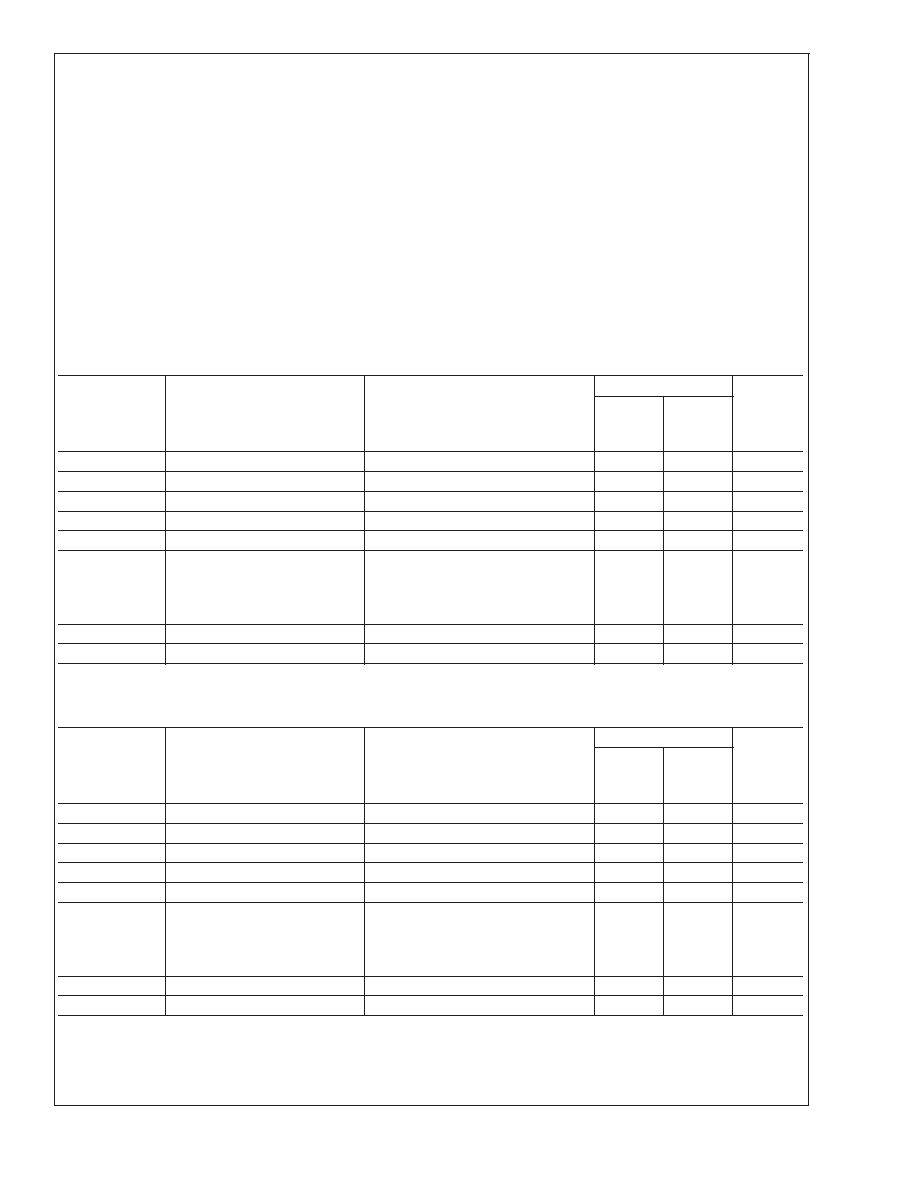
Electrical Characteristics V
DD
= 3.3V
(Notes 1, 2)
The following specifications apply for V
DD
= 3.3V, A
V
= 1, and 32
load unless otherwise specified. Limits apply to T
A
= 25�C.
Symbol
Parameter
Conditions
LM4910
Units
(Limits)
Typ
(Note 6)
Limit
(Notes 7,
8)
I
DD
Quiescent Power Supply Current
V
IN
= 0V, 32
Load
3.5
6
mA (max)
I
SD
Standby Current
V
SHUTDOWN
= GND
0.1
1.0
�A (max)
V
OS
Output Offset Voltage
5
30
mV (max)
P
O
Output Power
THD = 1% (max); f = 1kHz
35
30
mW (min)
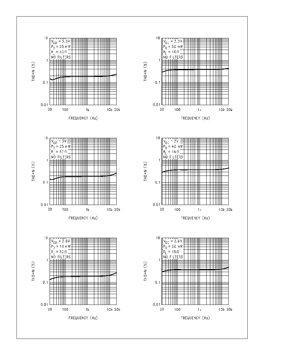
THD+N
Total Harmonic Distortion + Noise P
O
= 30mW
rms
; f = 1kHz
0.3
%
PSRR
Power Supply Rejection Ratio
V
RIPPLE
= 200mV
p-p
sinewave
Input terminated with 10
to ground
65 (f =
217Hz)
65 (f =
1kHz)
dB
V
IH
Shutdown Input Voltage High
1.5
V (min)
V
IL
Shutdown Input Voltage Low
0.4
V (max)
Electrical Characteristics V
DD
= 3V
(Notes 1, 2)
The following specifications apply for V
DD
= 3V, A
V
= 1, and 32
load unless otherwise specified. Limits apply to T
A
= 25�C.
Symbol
Parameter
Conditions
LM4910
Units
(Limits)
Typ
(Note 6)
Limit
(Notes 7,
8)
I
DD
Quiescent Power Supply Current
V
IN
= 0V, 32
Load
3.3
6
mA (max)
I
SD
Standby Current
V
SHUTDOWN
= GND
0.1
1.0
�A (max)
V
OS
Output Offset Voltage
5
30
mV (max)
P
O
Output Power
THD = 1% (max); f = 1kHz
30
25
mW (min)
THD+N
Total Harmonic Distortion + Noise P
O
= 25mW
rms
; f = 1kHz
0.3
%
PSRR
Power Supply Rejection Ratio
V
RIPPLE
= 200mV
p-p
sinewave
Input terminated with 10
to ground
65 (f =
217 Hz)
65 (f =
1kHz)
dB
V
IH
Shutdown Input Voltage High
1.5
V (min)
V
IL
Shutdown Input Voltage Low
0.4
V (max)
LM4910
www.national.com
3
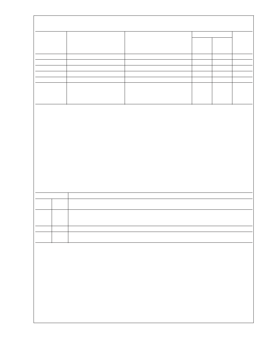
Electrical Characteristics V
DD
= 2.6V
(Notes 1, 2)
The following specifications apply for V
DD
= 2.6V, A
V
= 1, and 32
load unless otherwise specified. Limits apply to T
A
= 25�C.
Symbol
Parameter
Conditions
LM4910
Units
(Limits)
Typ
(Note 6)
Limit
(Notes 7,
8)
I
DD
Quiescent Power Supply Current
V
IN
= 0V, 32
Load
3.0
mA (max)
I
SD
Standby Current
V
SHUTDOWN
= GND
0.1
�A (max)
V
OS
Output Offset Voltage
5
mV (max)
P
O
Output Power
THD = 1% (max); f = 1kHz
13
mW
THD+N
Total Harmonic Distortion + Noise P
O
= 10mW
rms
; f = 1kHz
0.3
%
PSRR
Power Supply Rejection Ratio
V
RIPPLE
= 200mV
p-p
sinewave
Input terminated with 10
to ground
55 (f =
217Hz)
55 (f =
1kHz)
dB
Note 1: All voltages are measured with respect to the GND pin unless otherwise specified.
Note 2: Absolute Maximum Ratings indicate limits beyond which damage to the device may occur. Operating Ratings indicate conditions for which the device is
functional but do not guarantee specific performance limits. Electrical Characteristics state DC and AC electrical specifications under particular test conditions which
guarantee specific performance limits. This assumes that the device is within the Operating Ratings. Specifications are not guaranteed for parameters where no limit
is given, however, the typical value is a good indication of device performance.
Note 3: The maximum power dissipation must be derated at elevated temperatures and is dictated by T
JMAX
,
JA
, and the ambient temperature, T
A
. The maximum
allowable power dissipation is P
DMAX
= (T
JMAX
- T
A
)/
JA
or the number given in Absolute Maximum Ratings, whichever is lower. For the LM4910, see power derating
currents for more information.
Note 4: Human body model, 100pF discharged through a 1.5k
resistor.
Note 5: Machine Model, 220pF-240pF discharged through all pins.
Note 6: Typicals are measured at 25�C and represent the parametric norm.
Note 7: Limits are guaranteed to National's AOQL (Average Outgoing Quality Level).
Note 8: Datasheet min/max specification limits are guaranteed by design, test, or statistical analysis.
Note 9: If the product is in shutdown mode and V
DD
exceeds 6V (to a max of 8V V
DD
) then most of the excess current will flow through the ESD protection circuits.
If the source impedance limits the current to a max of 10ma then the part will be protected. If the part is enabled when V
DD
is above 6V circuit performance will be
curtailed or the part may be permanently damaged.
Note 10: Human body model, 100pF discharged through a 1.5k
resistor, Pin 6 to ground.
External Components Description
(Figure 1)
Components
Functional Description
1.
R
I
Inverting input resistance which sets the closed-loop gain in conjunction with R
f
. This resistor also forms a
high-pass filter with C
i
at f
c
= 1/(2
R
i
C
i
).
2.
C
I
Input coupling capacitor which blocks the DC voltage at the amplifier's input terminals. Also creates a
high-pass filter with R
i
at f
c
= 1/(2
R
i
C
i
). Refer to the section Proper Selection of External Components, for
an explanation of how to determine the value of C
i
.
3.
R
f
Feedback resistance which sets the closed-loop gain in conjunction with R
i
.
4.
C
S
Supply bypass capacitor which provides power supply filtering. Refer to the Power Supply Bypassing
section for information concerning proper placement and selection of the supply bypass capacitor.
LM4910
www.national.com
4