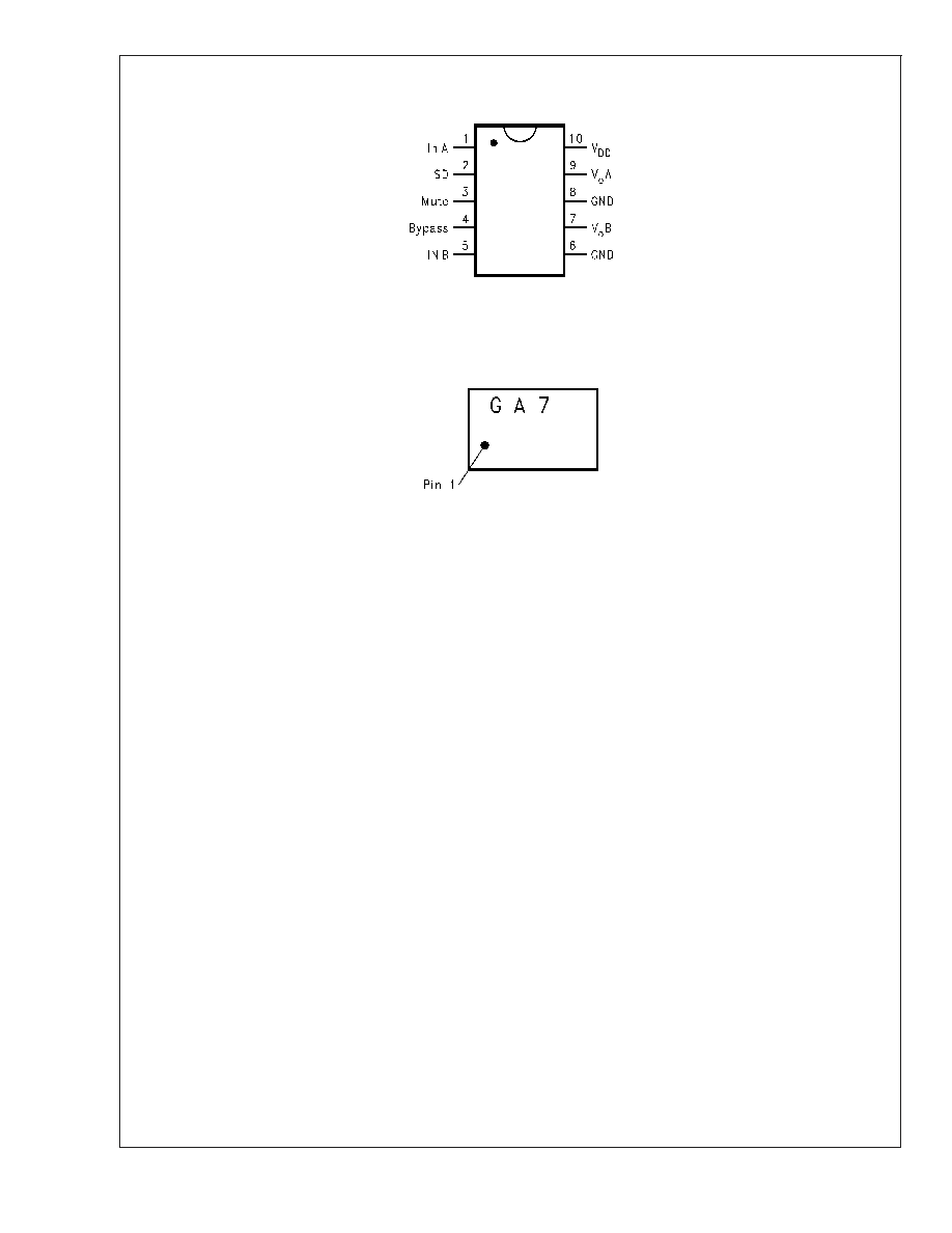
LM4912
Stereo 40mW Low Noise Headphone Amplifier
General Description
The LM4912 is an stereo audio power amplifier capable of
delivering 40mW per channel of continuous average power
into a 16
load or 25mW per channel into a 32 load at 1%
THD form a 3V power supply.
Boomer audio power amplifiers were designed specifically to
provide high quality output power with a minimal amount of
external components. Since the LM4912 does not require
bootstrap capacitors or snubber networks, it is optimally
suited for low-power portable systems.
The LM4912 features a low-power consumption shutdown
mode and a power mute mode that allows for faster turn on
time with less than 1mV voltage change at outputs on re-
lease. Additionally, the LM4912 features an internal thermal
shutdown protection mechanism.
The LM4912 is unity gain stable and may be configured with
external gain-setting resistors.
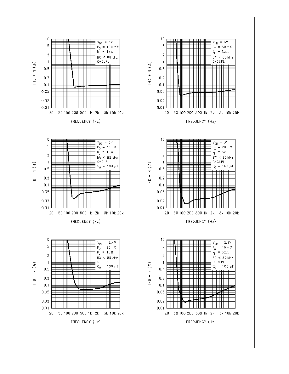
Key Specifications
n
PSRR at 217 Hz and 1kHz
65dB (typ)
n
Output Power at 1kHz with V
DD
= 2.4V, 1% THD+N into
a 16
load
25mW (typ)
n
Output Power at 1kHz with V
DD
= 3V, 1% THD+N into a
16
load
40mW (typ)
n
Shutdown Current
1.0�A (max)
n
Output Voltage change on release from Shutdown
V
DD
= 2.4V, R
L
= 16
1mV (max)
n
Output Noise, 20Hz to 20kHz, A-weighted
10�V (typ)
Features
n
External gain-setting capability
n
Available in space-saving MSOP package
n
Ultra low current shutdown mode
n
Mute mode allows fast turn-on (10ms) with less than
1mV change on outputs
n
2.0V - 5.5V operation
n
Ultra low noise
n
Operation at low supply voltages
Applications
n
Portable CD players
n
PDAs
n
Portable electronics devices
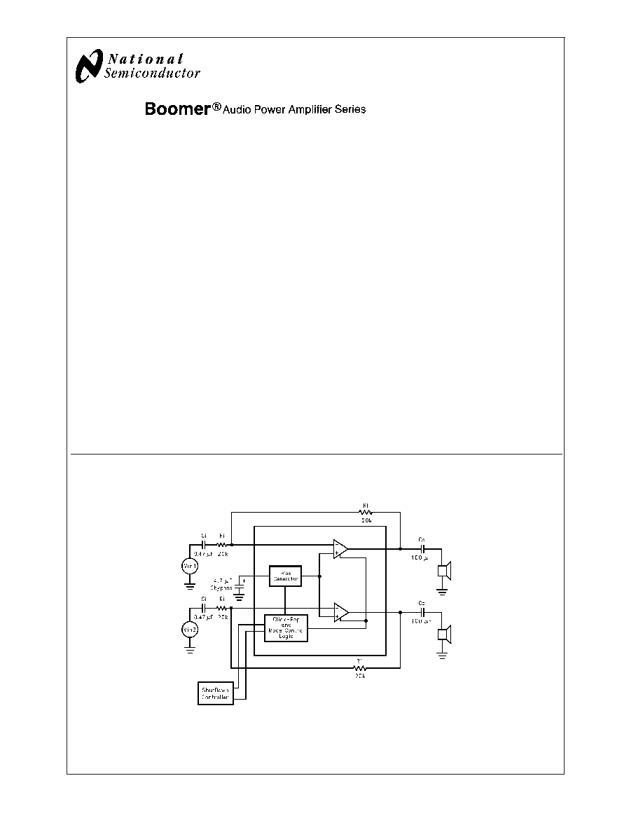
Typical Application
Boomer
�
is a registered trademark of National Semiconductor Corporation.
20048180
FIGURE 1. Typical Capacitive Coupled Output Configuration Circuit
June 2003
LM4912
Stereo
40mW
Low
Noise
Headphone
Amplifier
� 2003 National Semiconductor Corporation
DS200481
www.national.com
Absolute Maximum Ratings
(Note 2)
If Military/Aerospace specified devices are required,
please contact the National Semiconductor Sales Office/
Distributors for availability and specifications.
Supply Voltage
4.0V
Storage Temperature
-65�C to +150�C
Input Voltage
-0.3V to V
DD
+ 0.3V
Power Dissipation (Note 3)
Internally Limited
ESD Susceptibility (Note 4)
2000V
ESD Susceptibility (Note 5)
250V
Junction Temperature
150�C
Thermal Resistance
JC
(MSOP)
56�C/W
JA
(MSOP)
190�C/W
Operating Ratings
Temperature Range
T
MIN
T
A
T
MAX
-40�C
T
A
85�C
Supply Voltage (V
DD
)
2.0V
V
DD
5.5V
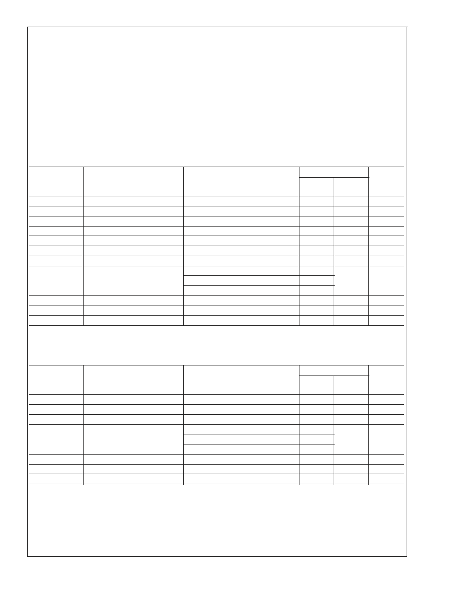
Electrical Characteristics V
DD
= 5.0V
(Notes 1, 2)
The following specifications apply for V
DD
= 5.0V, R
L
= 16
, C
O
= 100�, and C
B
= 4.7�F unless otherwise specified. Limits
apply to T
A
= 25�C.
Symbol
Parameter
Conditions
LM4912
Units
(Limits)
Typ
(Note 6)
Limit
(Note 7)
I
DD
Quiescent Power Supply Current
V
IN
= 0V, I
O
= 0A
2
5
mA (max)
I
SD
Shutdown Current
V
SHUTDOWN
= GND
0.1
2.0
�A (max)
I
M
Mute Current
V
MUTE
= V
DD
2
5
mA (max)
V
SDIH
Shutdown Voltage Input High
1.8
V
V
SDIL
Shutdown Voltage Input Low
0.4
V
V
MIH
Mute Voltage Input High
1.8
V
V
MIL
Mute Voltage Input Low
0.4
V
P
O
Output Power
THD = 1%; f = 1kHz
mW
R = 16
145
R = 32
80
V
NO
Output Noise Voltage
BW = 20 Hz to 20kHz, A-weighted
10
�V
PSRR
Power Supply Rejection Ratio
V
RIPPLE
= 200mV sine p-p
65
dB
A
M
Mute Attenuation
f = 1kHz
85
dB
Electrical Characteristics V
DD
= 3.0V
(Notes 1, 2)
The following specifications apply for V
DD
= 3.0V, R
L
= 16
, C
O
= 100�F, and C
B
= 4.7�F unless otherwise specified. Limits
apply to T
A
= 25�C.
Symbol
Parameter
Conditions
LM4912
Units
(Limits)
Typ
(Note 6)
Limit
(Note 7)
I
DD
Quiescent Power Supply Current
V
IN
= 0V, I
O
= 0A
1.5
3
mA (max)
I
SD
Shutdown Current
V
SHUTDOWN
= GND
0.1
2.0
�A (max)
I
M
Mute Current
V
MUTE
= V
DD
1.5
3
mA (max)
P
O
Output Power
THD = 1%; f = 1kHz
mW
R = 16
40
R = 32
25
V
NO
Output Noise Voltage
BW = 20 Hz to 20kHz, A-weighted
10
�V
PSRR
Power Supply Rejection Ratio
V
RIPPLE
= 200mV sine p-p
65
dB
A
M
Mute Attenuation
f = 1kHz
80
dB
LM4912
www.national.com
3
Electrical Characteristics V
DD
= 2.4V
(Notes 1, 2)
The following specifications apply for V
DD
= 2.4V, R
L
= 16
, C
O
= 100�F, and C
B
= 4.7�F unless otherwise specified. Limits
apply to T
A
= 25�C.
Symbol
Parameter
Conditions
LM4912
Units
(Limits)
Typ
(Note 6)
Limit
(Note 7)
I
DD
Quiescent Power Supply Current
V
IN
= 0V, I
O
= 0A
1.5
3
mA (max)
I
SD
Shutdown Current
V
SHUTDOWN
= GND
0.1
2.0
�A (max)
I
M
Mute Current
V
MUTE
= V
DD
1.5
3
mA (max)
P
O
Output Power
THD = 1%; f = 1kHz
mW
R = 16
25
R = 32
12
V
NO
Output Noise Voltage
BW = 20 Hz to 20kHz, A-weighted
10
�V
PSRR
Power Supply Rejection Ratio
V
RIPPLE
= 200mV sine p-p
65
dB
T
WU
Wake Up Time from Shutdown
2
s
V
OSD
Output Voltage Change on
Release from Shutdown
1
mV (max)
T
UM
Time to Un-Mute
0.01
0.02
s (max)
A
M
Mute Attenuation
f = 1kHz
80
db
Note 1: All voltages are measured with respect to the GND pin unless otherwise specified.
Note 2: : Absolute Maximum Ratings indicate limits beyond which damage to the device may occur. Operating Ratings indicate conditions for which the device is
functional but do not guarantee specific performance limits. Electrical Characteristics state DC and AC electrical specifications under particular test conditions which
guarantee specific performance limits. This assumes that the device is within the Operating Ratings. Specifications are not guaranteed for parameters where no limit
is given, however, the typical value is a good indication of device performance.
Note 3: : The maximum power dissipation must be derated at elevated temperatures and is dictated by TJMAX,
JA
, and the ambient temperature, T
A
. The
maximum allowable power dissipation is P
DMAX
= (T
JMAX
- T
A
)/
JA
or the number given in Absolute Maximum Ratings, whichever is lower. For the LM4912, see
power derating currents for more information.
Note 4: Human body model, 100pF discharged through a 1.5k
resistor.
Note 5: Machine Model, 220pF-240pF discharged through all pins.
Note 6: Typicals are measured at 25�C and represent the parametric norm.
Note 7: Limits are guaranteed to National's AOQL (Average Outgoing Quality Level).
Note 8: Datasheet min/max specification limits are guaranteed by design, test, or statistical analysis.
Note 9: 10
Terminated input.
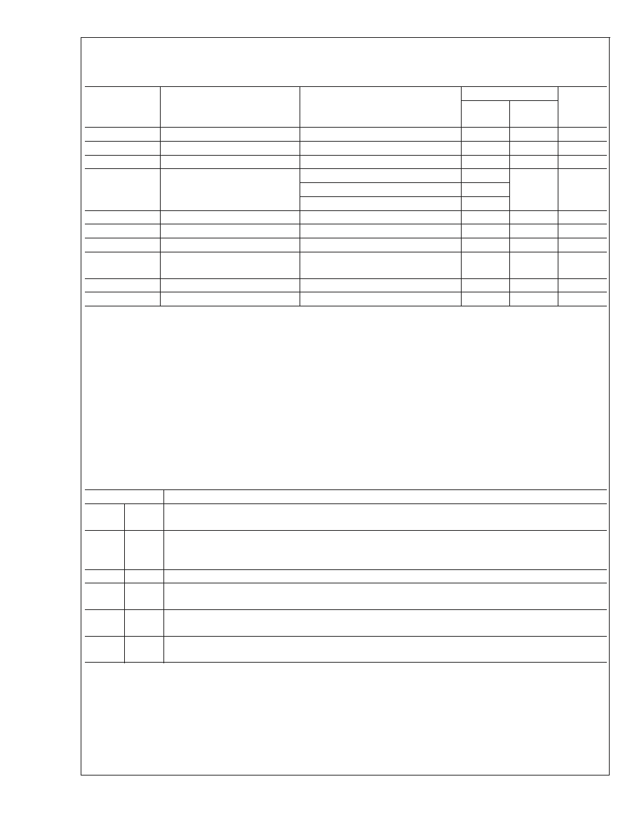
External Components Description
See (Figure 1)
Components
Functional Description
1.
R
I
Inverting input resistance which sets the closed-loop gain in conjunction with R
f
. This resistor also forms a
high-pass filter with C
i
at f
c
= 1/(2
R
i
C
i
).
2.
C
I
Input coupling capacitor which blocks the DC voltage at the amplifier's input terminals. Also creates a
high-pass filter with R
i
at f
c
= 1/(2
R
i
C
i
). Refer to the section Proper Selection of External Components, for
an explanation of how to determine the value of C
i
.
3.
R
f
Feedback resistance which sets the closed-loop gain in conjunction with R
i
.
4.
C
S
Supply bypass capacitor which provides power supply filtering. Refer to the Power Supply Bypassing
section for information concerning proper placement and selection of the supply bypass capacitor.
5.
C
B
Bypass pin capacitor which provides half-supply filtering. Refer to the section, Proper Selection of Proper
Components, for information concerning proper placement and selection of C
B
6.
C
o
Output coupling capacitor which blocks the DC voltage at the amplifier's output. Forms a high pass filter with
R
L
at f
o
= 1/(2
R
L
C
o
)
LM4912
www.national.com
4