 | ÐлекÑÑоннÑй компоненÑ: LM4914MHX | СкаÑаÑÑ:  PDF PDF  ZIP ZIP |
LM4914 Boomer ® Audio Power Amplifier Series 1W Monaural, 85mW Stereo Headphone Audio Amplifier
LM4914
1W Monaural, 85mW Stereo Headphone Audio Amplifier
General Description
The unity-gain stable LM4914 is both a mono differential
output (for bridge-tied loads, or BTL) audio power amplifier
and a single-ended (SE) stereo headphone amplifier. Oper-
ating on a single 5V supply, the mono BTL mode delivers 1W
into an 8
load. In SE stereo mode, the amplifier delivers
85mW to 32
loads. The LM4914 features circuitry that
suppresses output transients ("clicks and pops").
The LM4914 is designed for notebook and other handheld
portable applications. It delivers high quality output power
from a surface-mount package and requires few external
components. The LM4914 is pin and functionally compatible
with the TPA0253.
Other features include an active-low micro-power shutdown
mode and thermal shutdown protection.
The LM4914 is available in a space efficient 10-lead
exposed-DAP TSSOP package.
Key Specifications
j
BTL output power (R
L
= 8
)
V
DD
= at 3.0V, THD = 0.1%
V
DD
= at 5.0V, THD = 0.1%
330mW (typ)
1W (typ)
j
SE output power (R
L
= 32
)
V
DD
= at 3.0V, THD = 0.1%
V
DD
= at 5.0V, THD = 0.1%
30mW (typ)
85mW (typ)
j
Micro-power shutdown supply current
0.03µA (typ)
j
PSRR (f = 1kHz)
V
DD
= at 3.0V, BTL Mode
V
DD
= at 5.0V, BTL Mode
52dB (typ)
52dB (typ)
Features
n
Advanced "click and pop" suppression circuitry
n
Stereo headphone amplifier mode
n
Low current micro-power shutdown mode
n
Thermal shutdown protection circuitry
n
2.5V to 5.5V operation
n
Unity-gain stable
n
Gain set with external resistors
n
Space-saving exposed-DAP TSSOP package
Applications
n
PDAs
n
Cellular phones
n
Handheld portable electronic devices
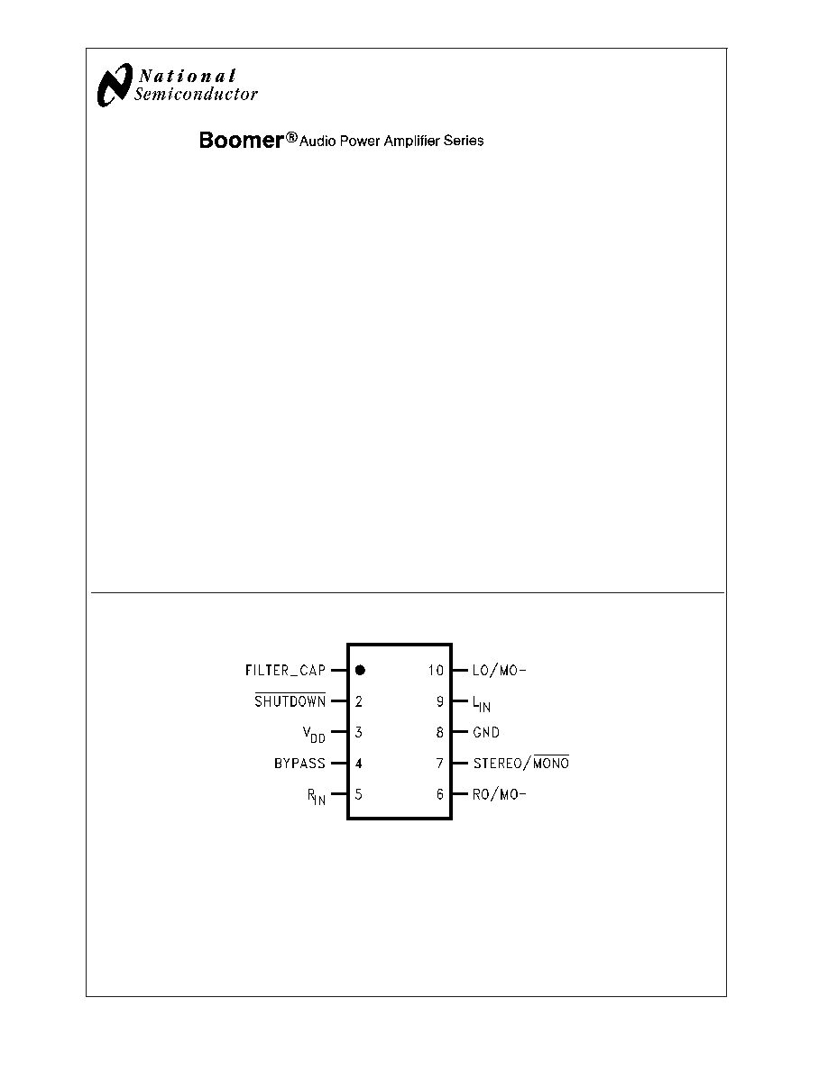
Connection Diagram
200634A0
Top View
Order Number LM4914MH
See NS package Number MXF10A
Boomer
®
is a registered trademark of National Semiconductor Corporation.
March 2003
LM4914
1W
Monaural,
85mW
Stereo
Headphone
Audio
Amplifier
© 2003 National Semiconductor Corporation
DS200634
www.national.com
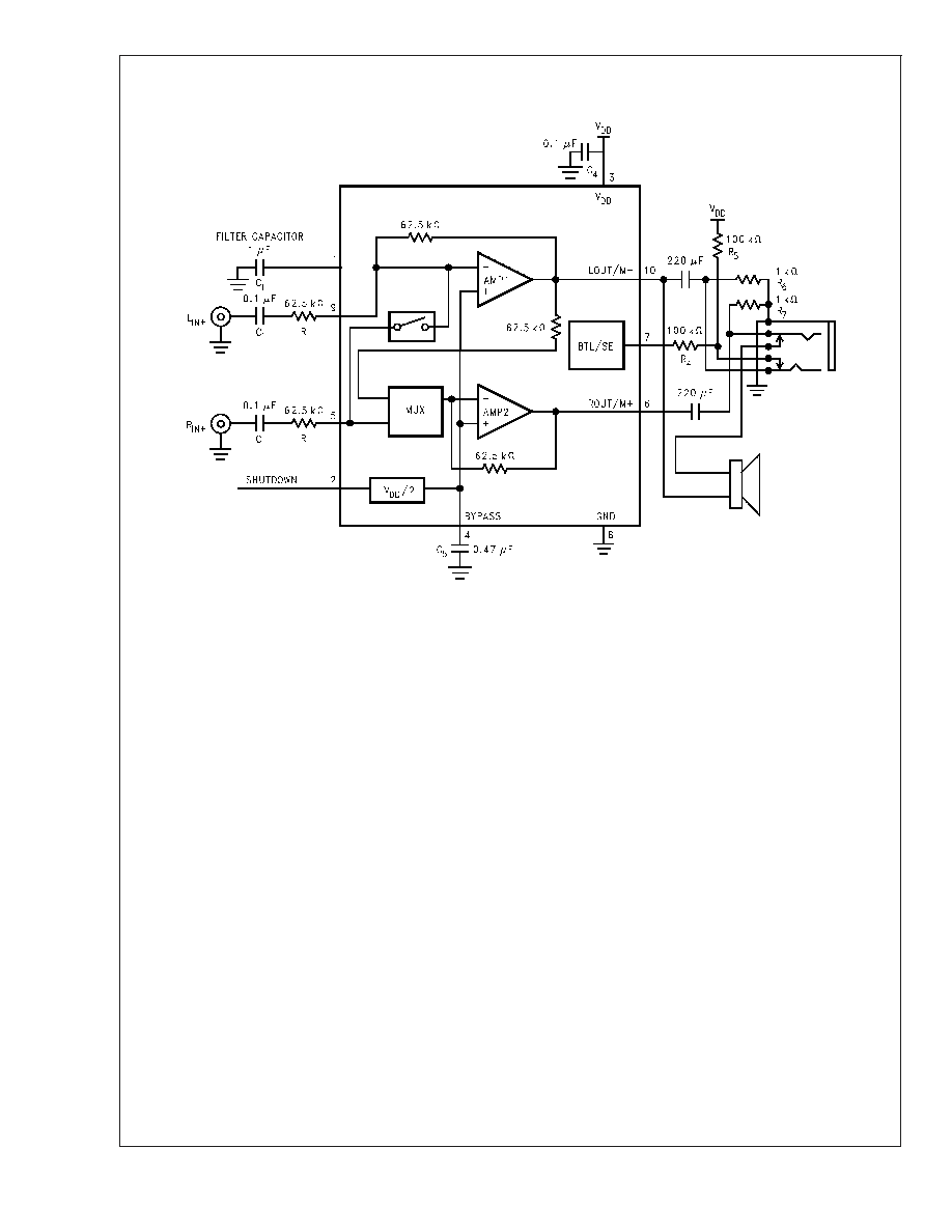
Typical Application
200634C3
FIGURE 1. Typical Audio Amplifier Application Circuit
LM4914
www.national.com
2
Absolute Maximum Ratings
(Note 3)
If Military/Aerospace specified devices are required,
please contact the National Semiconductor Sales Office/
Distributors for availability and specifications.
Supply Voltage
6.0V
Storage Temperature
-65°C to +150°C
Input Voltage
-0.3V to V
DD
+0.3V
Power Dissipation (Note 4)
Internally Limited
ESD Susceptibility (Note 5)
2000V
ESD Susceptibility (Note 6)
200V
Junction Temperature
150°C
Solder Information
Small Outline Package
Vapor Phase (60sec)
215°C
Infrared (15sec)
220°C
See AN-450 "Surface Mounting
and their Effects on Product
Reliability" for other methods of
soldering surface-mount devices.
Thermal Resistance
JA
(typ) - MXF10A
46°C/W
Operating Ratings
Temperature Range
T
MIN
T
A
T
MAX
-40°C
T
A
85°C
Supply Voltage
2.5V
V
DD
5.5V
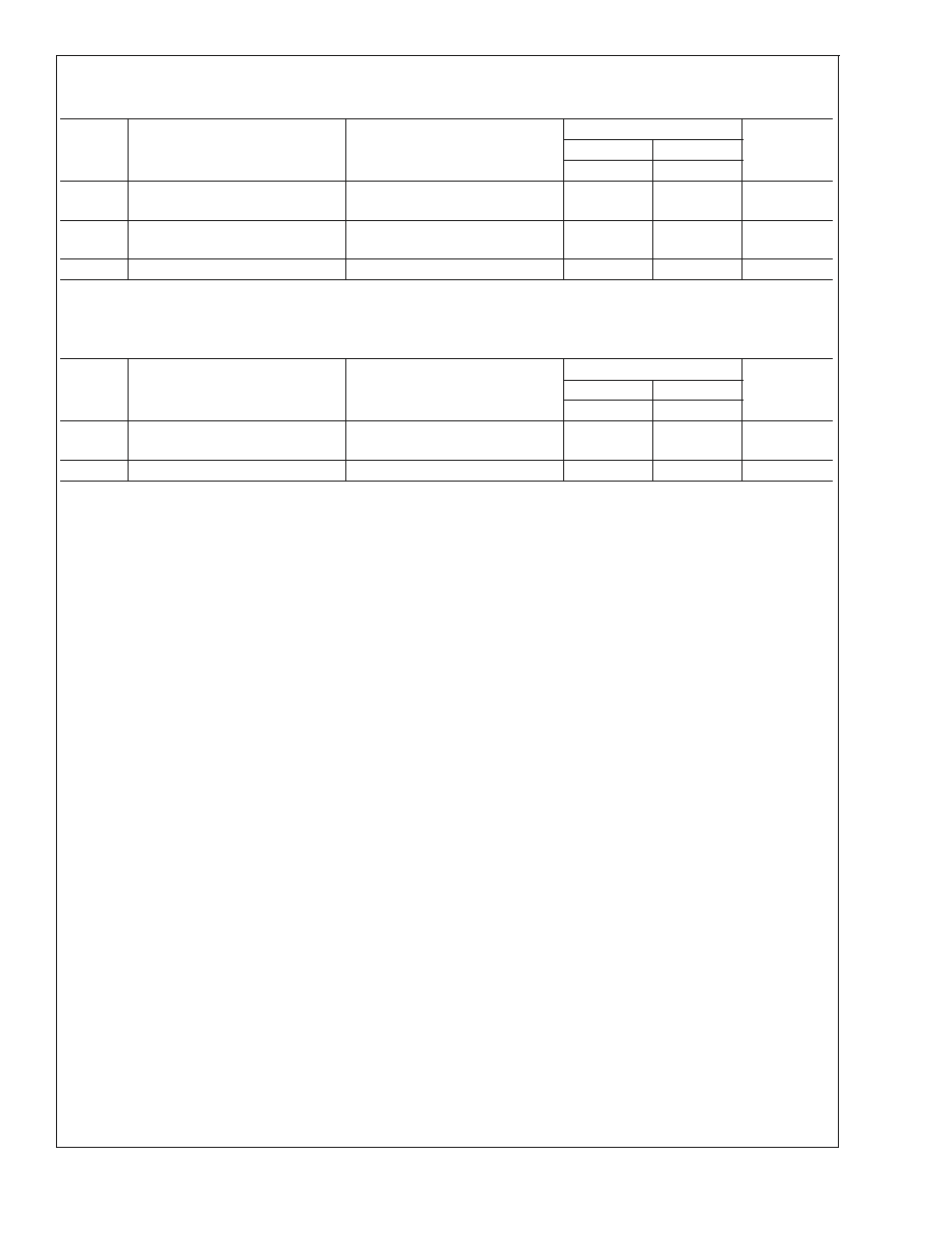
Electrical Characteristics for Entire Amplifier (V
DD
= 5V)
(Note 3)
The following specifications apply for the circuit shown in Figure 1, unless otherwise specified. Limits apply for T
A
= 25°C.
Symbol
Parameter
Conditions
LM4914
Units
(Limits)
Typical
Limit
(Note 8)
(Notes 9, 10)
V
DD
Supply Voltage
2.5
5.5
V (min)
V (max)
I
DD
Quiescent Power Supply Current
V
IN
= 0V, I
O
= 0A, No Load
4
6.5
mA (max)
I
SD
Shutdown Quiescent Power Supply
Current
V
SHUTDOWN
= GND
0.03
5
µA (max)
V
OS
Output Offset Voltage
7
30
mV (max)
PSRR
Power Supply Rejection Ratio
V
DD
= 5V, C
BYPASS
= 0.47µF,
V
ripple
= 200mVp-p 1kHz sine wave
R
L
= 8
52 BTL
60 SE
dB
HP-S
VIH
HP-SENSE Logic-High Threshold
Voltage
4.5
V (min)
HP-S
VIL
HP-SENSE Logic-Low Threshold
Voltage
2.75
V (max)
SD
VIH
Shutdown Logic High Threshold
2.0
V (min)
SD
VIL
Shutdown Logic LowThreshold
0.8
V (max)
LM4914
www.national.com
3
Electrical Characteristics: Bridged-Mode Operation (V
DD
= 5V)
(Note 3)
The following specifications apply for the circuit shown in Figure 1, R
L
= 8
, and a measurement bandwidth of 20Hz to
80kHz, unless otherwise specified. Limits apply for T
A
= 25°C.
Symbol
Parameter
Conditions
LM4914
Units
(Limits)
Typical
Limit
(Note 8)
(Notes 9, 10)
P
O
Output Power (Note 1, 11)
R
L
= 8
, f = 1kHz,
THD+N = 0.1%, A
V
= 8dB
1
W (min)
THD+N
Total Harmonic Distortion + Noise
R
L
= 8
, f = 1kHz, P
O
= 1W
0.33
%
V
ON
Output Voltage Noise
C
B
= 0.47µF, 20Hz
<
f
<
20kHz
35
µV
RMS
Electrical Characteristics: SE Operation (V
DD
= 5V)
(Note 3)
The following specifications apply for the circuit shown in Figure 1 and a measurement bandwidth of 20Hz to 80kHz, unless
otherwise specified. Limits apply for T
A
= 25°C.
Symbol
Parameter
Conditions
LM4914
Units
(Limits)
Typical
Limit
(Note 8)
(Notes 9, 10)
P
O
Output Power (Note 11)
THD+N = 0.1%, f = 1kHz,
R
L
= 32
, A
V
= 1.9dB (Note 12)
85
mW (min)
V
ON
Output Voltage Noise
C
B
= 0.47µF, 20Hz
<
f
<
20kHz
13
µV
RMS
Electrical Characteristics for Entire Amplifier (V
DD
= 3V)
(Note 3)
The following specifications apply for the circuit shown in Figure 1, unless otherwise specified. Limits apply for T
A
= 25°C.
Symbol
Parameter
Conditions
LM4914
Units
(Limits)
Typical
Limit
(Note 8)
(Notes 9, 10)
V
DD
Supply Voltage
2.5
5.5
V (min)
V (max)
I
DD
Quiescent Power Supply Current
V
IN
= 0V, I
O
= 0A, No Load
2.7
5
mA (max)
I
SD
Shutdown Quiescent Power Supply
Current
V
SHUTDOWN
= GND
0.03
4
µA (max)
V
OS
Output Offset Voltage
7
30
mV (max)
PSRR
Power Supply Rejection Ratio
V
DD
= 3V, C
BYPASS
= 0.47µF,
V
ripple
= 200mVp-p 1kHz sine wave
R
L
= 8
52 BTL
60 SE
dB
HP-S
VIH
HP-SENSE Logic-High Threshold
Voltage
2.7
V (min)
HP-S
VIL
HP-SENSE Logic-Low Threshold
Voltage
1.65
V (max)
SD
VIH
Shutdown Logic High Threshold
2
V (min)
SD
VIL
Shutdown Logic LowThreshold
0.8
V (max)
LM4914
www.national.com
4
Electrical Characteristics: Bridged-Mode Operation (V
DD
= 3V)
(Note 3)
The following specifications apply for the circuit shown in Figure 1, unless otherwise specified. Limits apply for T
A
= 25°C.
Symbol
Parameter
Conditions
LM4914
Units
(Limits)
Typical
Limit
(Note 8)
(Notes 9, 10)
P
O
Output Power (Note 11)
THD = 0.1%, f = 1kHz
A
V
= 14dB, R
L
= 8
330
mW
THD+N
Total Harmonic Distortion + Noise
f = 1kHz
P
O
= 250mW
0.2
%
V
ON
Output Voltage Noise
C
B
= 0.47µF, 20Hz
<
f
<
20kHz
29
µV
RMS
Electrical Characteristics: SE Operation (V
DD
= 3V)
(Note 3)
The following specifications apply for the circuit shown in Figure 1 and a measurement bandwidth of 20Hz to 80kHz, unless
otherwise specified. Limits apply for T
A
= 25°C.
Symbol
Parameter
Conditions
LM4914
Units
(Limits)
Typical
Limit
(Note 8)
(Notes 9, 10)
P
O
Output Power (Note 11)
THD+N = 0.1%, f = 1kHz,
R
L
= 32
, A
V
= 1.9dB (Note 12)
30
mW
V
ON
Output Voltage Noise
C
B
= 0.47µF, 20Hz
<
f
<
20kHz
13
µV
RMS
Note 1: When operating on a 5V
DC
, an LM4914MH that has been properly mounted to a circuit board will deliver 1W into 8
. See the Application Information
sections for further information concerning PCB layout suggestions to maximize the LM4914MH's output power into an 8
load.
Note 2: All voltages are measured with respect to the GND pin unless otherwise specified.
Note 3: Absolute Maximum Ratings indicate limits beyond which damage to the device may occur. Operating Ratings indicate conditions for which the device is
functional, but do not guarantee specific performance limits. Electrical Characteristics state DC and AC electrical specifications under particular test conditions which
guarantee specific performance limits. This assumes that the device is within the Operating Ratings. Specifications are not guaranteed for parameters where no limit
is given, however, the typical value is a good indication of device performance.
Note 4: The maximum power dissipation must be derated at elevated temperatures and is dictated by T
JMAX
,
JA
, and the ambient temperature T
A
. The maximum
allowable power dissipation is P
DMAX
= (T
JMAX
T
A
)/
JA
or the number given in Absolute Maximum Ratings, whichever is lower. For the LM4914, see power derating
curves for additional information.
Note 5: Human body model, 100pF discharged through a 1.5k
resistor.
Note 6: Machine Model, 220pF240pF discharged through all pins.
Note 7: The given
JA
is for an LM4914 packaged in an MH with the Exposed-DAP soldered to an exposed 2in
2
area of 1oz printed circuit board copper.
Note 8: Typicals are measured at 25°C and represent the parametric norm.
Note 9: Limits are guaranteed to National's AOQL (Average Outgoing Quality Level).
Note 10: Datasheet minimum and maximum specification limits are guaranteed by design, test, or statistical analysis.
Note 11: Output power is measured at the amplifier's package pins.
Note 12: See Application Information section "Single-Ended Output Power Performance and Measurement Considerations" for more information.
LM4914
www.national.com
5
Document Outline