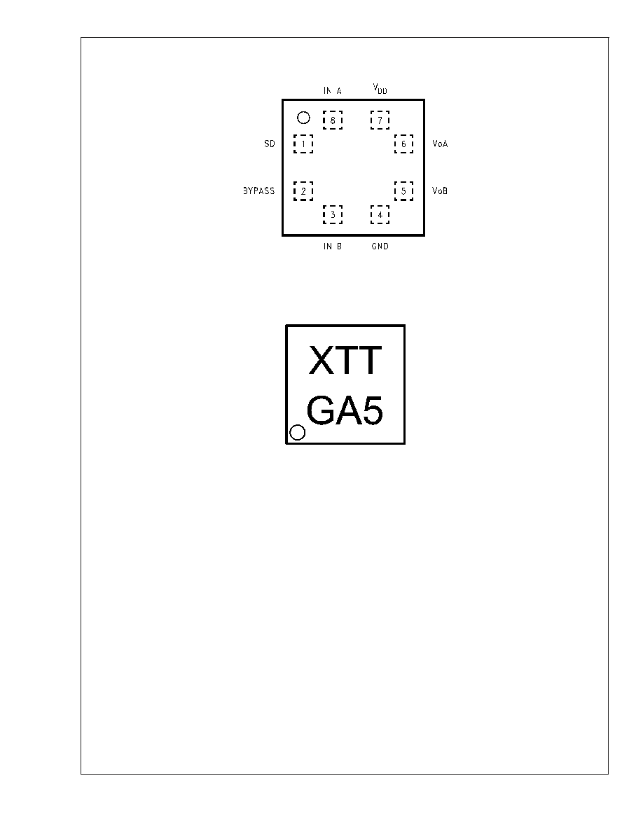
LM4915
Pseudo-Differential Mono Headphone Amplifier with
Fixed 6dB Gain
General Description
The LM4915 is a pseudo-differential audio power amplifier
primarily designed for demanding applications in mobile
phones and other portable audio device applications with
mono headphones. It is capable of delivering 90 miliwatts of
continuous average power to a 32
BTL load with less than
1% distortion (THD+N) from a 3V
DC
power supply.
Boomer audio power amplifiers were designed specifically to
provide high quality output power with a minimal amount of
external components. The LM4915 does not require output
coupling capacitors or bootstrap capacitors, and therefore is
ideally suited for mobile phone and other low voltage appli-
cations where minimal power consumption is a primary re-
quirement.
The LM4915 features a low-power consumption shutdown
mode. To facilitate this, Shutdown may be enabled by driving
the shutdown pin low. Additionally, the LM4915 features an
internal thermal shutdown protection mechanism.
The LM4915 contains advanced pop & click circuitry which
virtually eliminates noises which would otherwise occur dur-
ing turn-on and turn-off transitions.
The LM4915 has an internally fixed gain of 6dB.
Key Specifications
n
Improved PSRR at 217Hz and 1kHz
75dB (typ)
n
Power Output at 5.0V & 1% THD into 32
280mW (typ)
n
Power Output at 3.0V & 1% THD into 32
90mW (typ)
n
Output Noise, A-weighted
20�V (typ)
Features
n
Pseudo-differential amplification
n
Internal gain-setting resistors
n
Available in space-saving LLP package
n
Ultra low current shutdown mode
n
Can drive capacitive loads up to 500pF
n
Improved pop & click circuitry virtually eliminates noises
during turn-on and turn-off transitions
n
2.2 - 5.5V operation
n
No output coupling capacitors, snubber networks,
bootstrap capacitors or gain-setting resistors required
n
Ultra low noise
Applications
n
Mobile phones
n
PDAs
n
Portable electronics devices
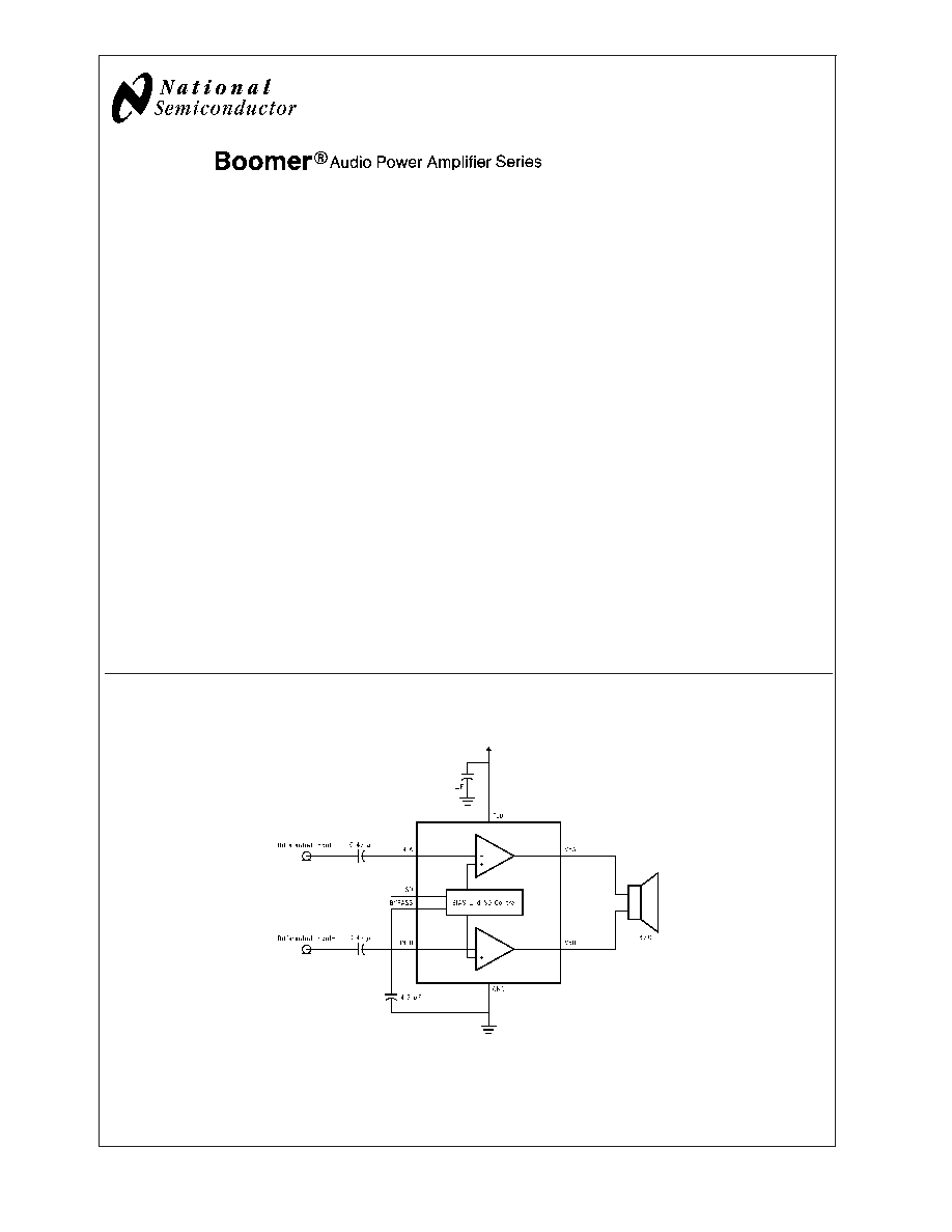
Typical Application
Boomer
�
is a registered trademark of National Semiconductor Corporation.
200482B4
FIGURE 1. Typical Audio Amplifier Application Circuit
May 2003
LM4915
Pseudo-Differential
Mono
Headphone
Amplifier
with
Fixed
6dB
Gain
� 2003 National Semiconductor Corporation
DS200482
www.national.com
Absolute Maximum Ratings
(Note 2)
If Military/Aerospace specified devices are required,
please contact the National Semiconductor Sales Office/
Distributors for availability and specifications.
Supply Voltage
6.0V
Storage Temperature
-65�C to +150�C
Input Voltage
-0.3V to V
DD
+ 0.3V
Power Dissipation (Note 3)
Internally Limited
ESD Susceptibility (Note 4)
2000V
ESD Susceptibility (Note 5)
200V
Junction Temperature
150�C
Thermal Resistance
JC
(LQ)
57�C/W
JA
(LQ)
140�C/W
Operating Ratings
Temperature Range
T
MIN
T
A
T
MAX
-40�C
T
A
+85�C
Supply Voltage (V
DD
)
2.2V
V
CC
5.5V
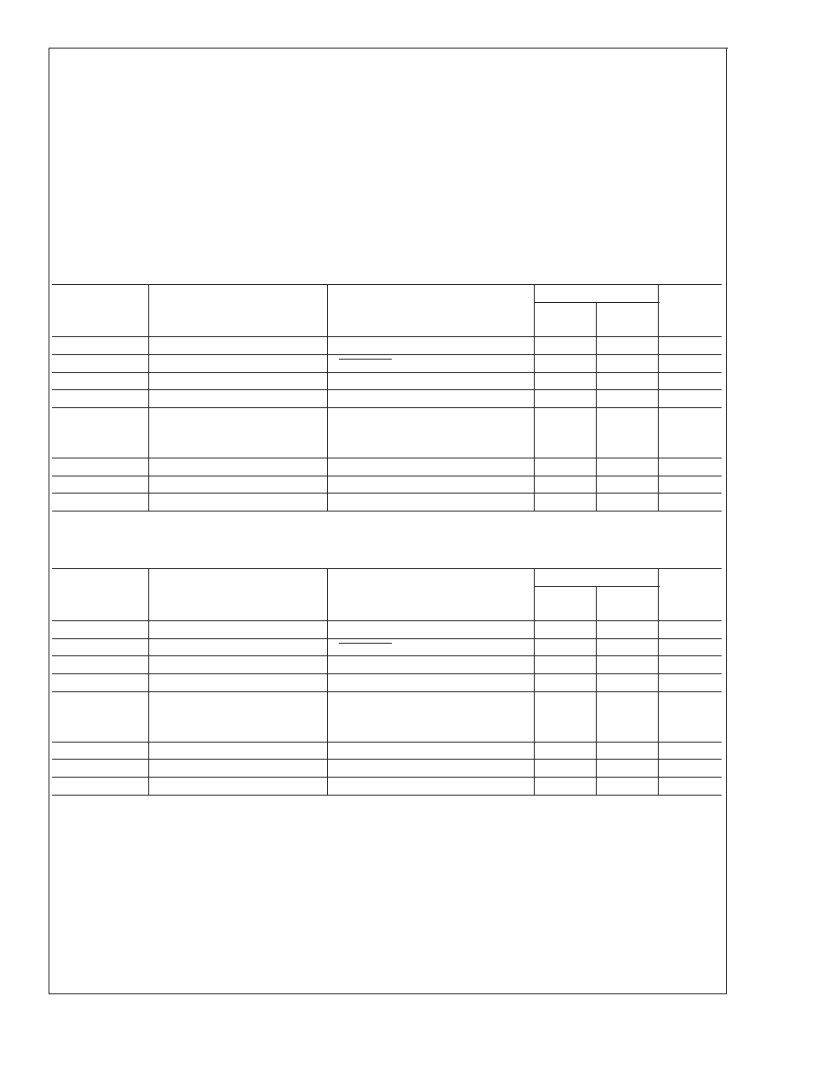
Electrical Characteristics V
DD
= 5V
(Notes 1, 2, 8)
The following specifications apply for V
DD
= 5V, R
L
= 16
unless otherwise specified. Limits apply to T
A
= 25�C.
Symbol
Parameter
Conditions
LM4915
Units
(Limits)
Typ
(Note 6)
Limit
(Note 7)
I
DD
Quiescent Power Supply Current
V
IN
= 0V, I
O
= 0A
2
3.5
mA (max)
I
SD
Shutdown Current
V
SHUTDOWN
= GND
0.1
Note 9
�A(max)
V
SDIH
Shutdown Voltage Input High
1.8
V
V
SDIL
Shutdown Voltage Input Low
0.4
V
P
O
Output Power
THD = 1% (max); f = 1kHz
R
L
= 16
R
L
= 32
400
280
375
250
mW
V
NO
Output Noise Voltage
BW = 20Hz to 20kHz, A-weighted
20
�V
PSRR
Power Supply Rejection Ratio
V
RIPPLE
= 200mV sine p-p
75
dB
V
OS
Output Offset Voltage
V
IN
= 0V
2
20
mV (max)
Electrical Characteristics V
DD
= 3.0V
(Notes 1, 2, 8)
The following specifications apply for V
DD
= 3.0V, R
L
= 16
unless otherwise specified. Limits apply to T
A
= 25�C.
Symbol
Parameter
Conditions
LM4915
Units
(Limits)
Typ
(Note 6)
Limit
(Note 7)
I
DD
Quiescent Power Supply Current
V
IN
= 0V, I
O
= 0A
1.5
2.5
mA (max)
I
SD
Shutdown Current
V
SHUTDOWN
= GND
0.1
Note 9
�A(max)
V
SDIH
Shutdown Voltage Input High
1.8
V
V
SDIL
Shutdown Voltage Input Low
0.4
V
P
O
Output Power
THD = 1% (max); f = 1kHz
R
L
= 16
R
L
= 32
125
90
100
80
mW (min)
V
NO
Output Noise Voltage
BW = 20Hz to 20kHz, A-weighted
20
�V
PSRR
Power Supply Rejection Ratio
V
RIPPLE
= 200mV sine p-p
70
dB
V
OS
Output Offset Voltage
V
IN
= 0V
2
20
mV (max)
Note 1: All voltages are measured with respect to the GND pin unless otherwise specified.
Note 2: Absolute Maximum Ratings indicate limits beyond which damage to the device may occur. Operating Ratings indicate conditions for which the device is
functional but do not guarantee specific performance limits. Electrical Characteristics state DC and AC electrical specifications under particular test conditions which
guarantee specific performance limits. This assumes that the device is within the Operating Ratings. Specifications are not guaranteed for parameters where no limit
is given, however, the typical value is a good indication of device performance.
Note 3: The maximum power dissipation must be derated at elevated temperatures and is dictated by T
JMAX
,
JA
, and the ambient temperature, T
A
. The maximum
allowable power dissipation is P
DMAX
= (T
JMAX
- T
A
)/
JA
or the number given in Absolute Maximum Ratings, whichever is lower. For the LM4915, see power derating
curves for more information.
Note 4: Human body model, 100pF discharged through a 1.5k
resistor.
Note 5: Machine Model, 220pF-240pF discharged through all pins.
Note 6: Typicals are measured at 25�C and represent the parametric norm.
Note 7: Limits are guaranteed to National's AOQL (Average Outgoing Quality Level).
Note 8: Datasheet min/max specifications are guaranteed by design, test, or statistical analysis.
LM4915
www.national.com
3
Electrical Characteristics V
DD
= 3.0V
(Notes 1, 2, 8) (Continued)
Note 9: See I
SD
distribution values shown in the I
SD
Distribution curve, V
DD
= 5V and V = 3V, shown in the Typical Performance Characteristics section.
External Components Description
(Figure 1)
Components
Functional Description
1.
C
B
Bypass pin capacitor that provides half-supply filtering. Refer to the section Proper Selection of External
Components for information concerning proper placement and selection of C
B
.
2.
C
i
Input coupling capacitor which blocks the DC voltage at the amplifier's input terminals. Also creates a
high-pass filter with the internal input resistance R
i
. For the LM4915, R
i
= 20k
, thus creating a high-pass
filter f
c
= 1/(2
R
i
C
i
). Refer to the section Proper Selection of External Components for an explanantion of
how to determine the value of C
i
.
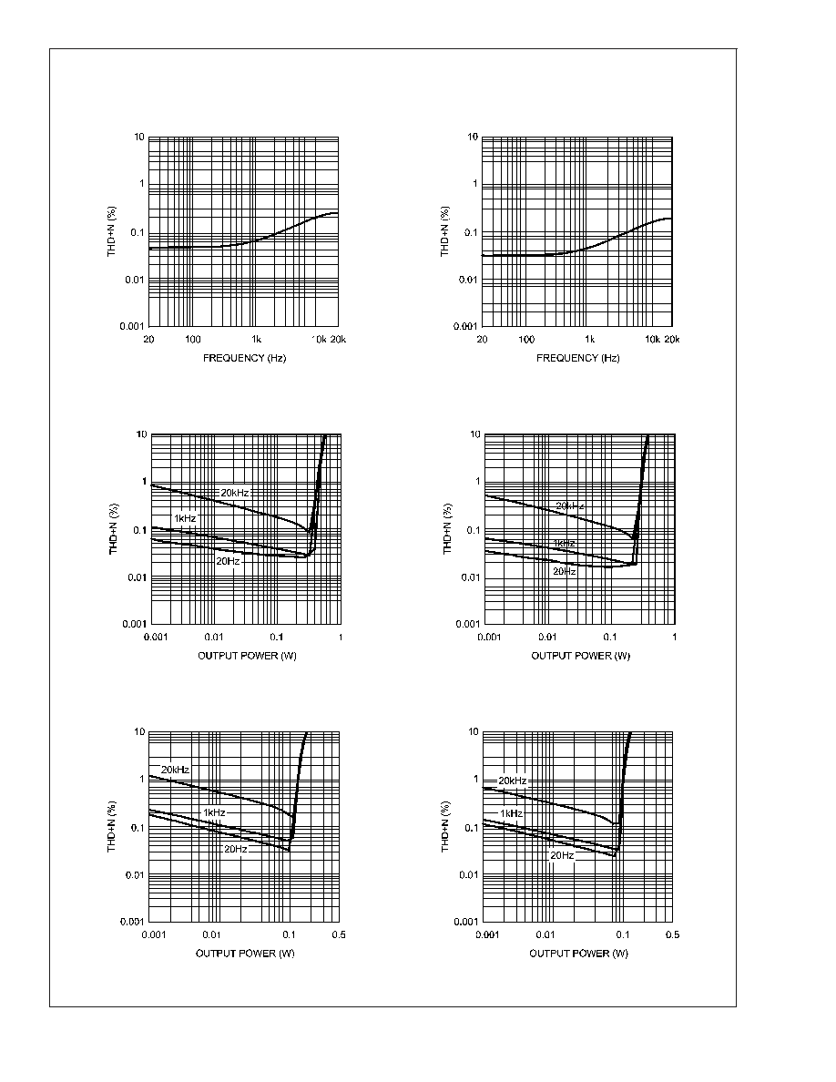
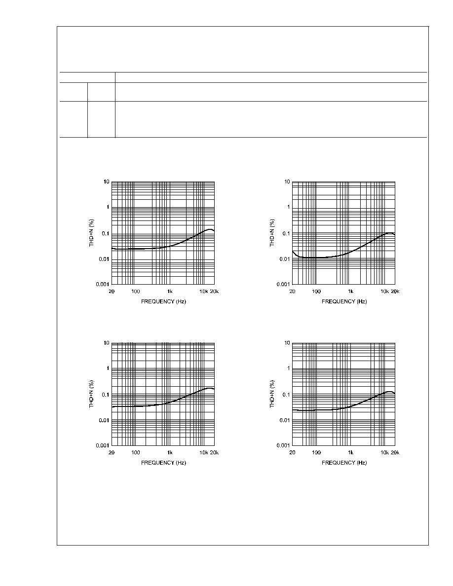
Typical Performance Characteristics
THD+N vs Frequency
V
DD
= 5V, R
L
= 16
THD+N vs Frequency
V
DD
= 5V, R
L
= 32
200482C6
200482C7
THD+N vs Frequency
V
DD
= 3V, R
L
= 16
, P
O
= 100mW
THD+N vs Frequency
V
DD
= 3V, R
L
= 32
, P
O
= 80mW
200482C4
200482C5
LM4915
www.national.com
4