 | –≠–ª–µ–∫—Ç—Ä–æ–Ω–Ω—ã–π –∫–æ–º–ø–æ–Ω–µ–Ω—Ç: LM4924MM | –°–∫–∞—á–∞—Ç—å:  PDF PDF  ZIP ZIP |
LM4924
2 Cell Battery, 40mW Per Channel Output Capacitor-Less
(OCL) Stereo Headphone Audio Amplifier
General Description
The LM4924 is a Output Capacitor-Less (OCL) stereo head-
phone amplifier, which when connected to a 3.0V supply,
delivers 40mW per channel to a 16
load with less than 1%
THD+N.
With the LM4924 packaged in the MM and SD packages, the
customer benefits include low profile and small size. These
packages minimizes PCB area and maximizes output power.
The LM4924 features circuitry that reduces output transients
("clicks" and "pops") during device turn-on and turn-off, and
Mute On and Off. An externally controlled, low-power con-
sumption, active-low shutdown mode is also included in the
LM4924. Boomer audio power amplifiers are designed spe-
cifically to use few external components and provide high
quality output power in a surface mount packages.
Key Specifications
n
OCL output power
n
(R
L
= 16
, V
DD
= 3.0V, THD+N = 1%)
40mW (typ)
n
Micropower shutdown current
0.1µA (typ)
n
Supply voltage operating range
1.5V
<
V
DD
<
3.6V
n
PSRR 100Hz, V
DD
= 3.0V, A
V
= 2.5
66dB (typ)
Features
n
2-cell 1.5V to 3.6V battery operation
n
OCL mode for stereo headphone operation
n
Unity-gain stable
n
"Click and pop" suppression circuitry for shutdown On
and Off transients
n
Active low micropower shutdown
n
Thermal shutdown protection circuitry
Applications
n
Portable two-cell audio products
n
Portable two-cell electronic devices
Typical Application
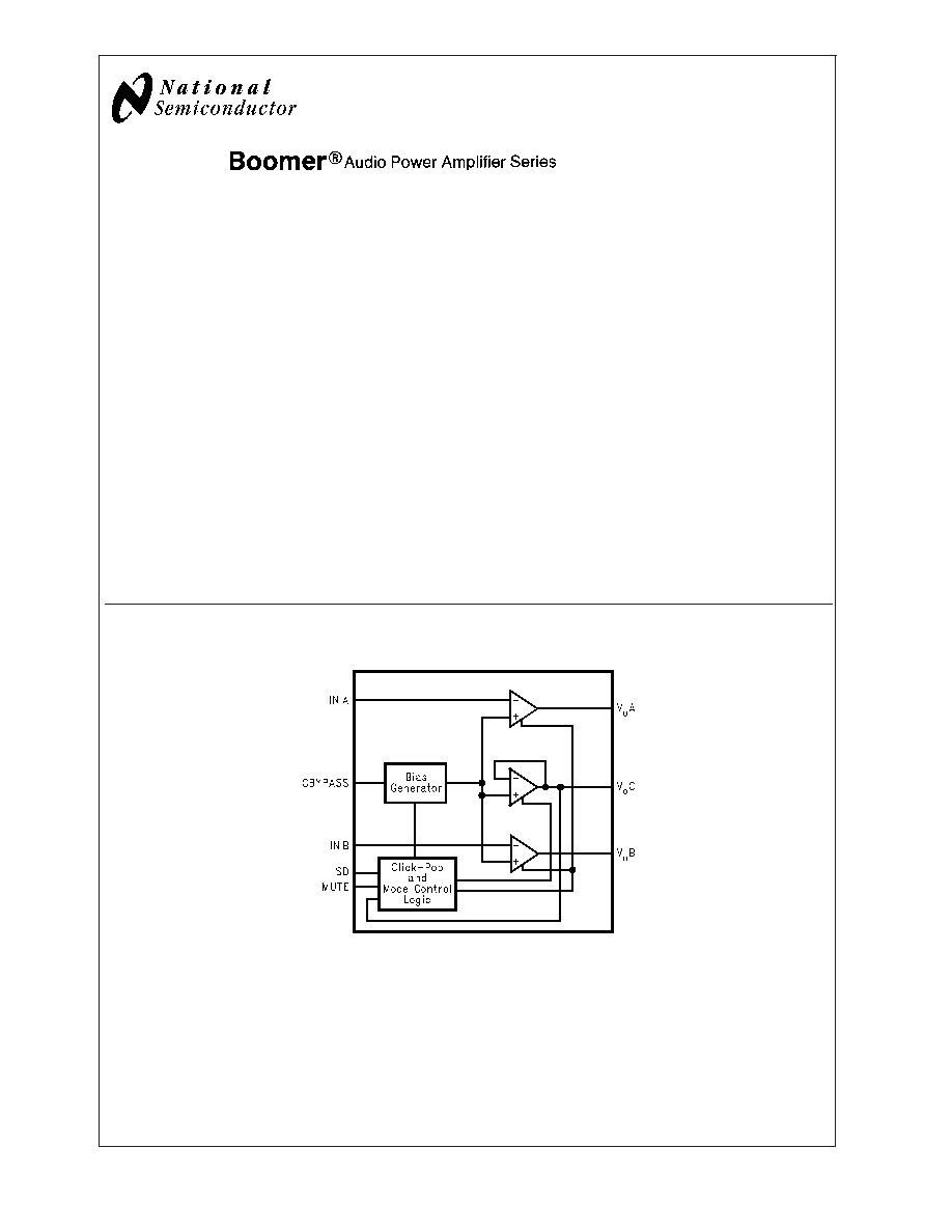
Boomer
Æ
is a registered trademark of National Semiconductor Corporation.
20121057
FIGURE 1. Block Diagram
October 2004
LM4924
2
Cell
Battery
,
40mW
Per
Channel
Output
Capacitor-Less
(OCL)
Stereo
Headphone
Audio
Amplifier
© 2004 National Semiconductor Corporation
DS201210
www.national.com
Connection Diagrams
MSOP Package
MSOP Marking
20121058
Top View
Order Number LM4924MM
See NS Package Number MUB10A for MSOP
20121006
Z- Plant Code
X - Date Code
T - Die Traceability
G - Boomer Family
B7 - LM4924MM
SD Package
SD Marking
20121052
Top View
Order Number LM4924SD
See NS Package Number SDA10A
20121007
Z - Plant Code
X - Date Code
T - Die Traceability
Bottom Line - Part Number
LM4924
www.national.com
2
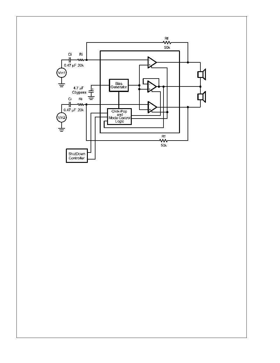
Typical Connections
20121059
FIGURE 2. Typical OCL Output Configuration Circuit
LM4924
www.national.com
3
Absolute Maximum Ratings
(Note 1)
If Military/Aerospace specified devices are required,
please contact the National Semiconductor Sales Office/
Distributors for availability and specifications.
Supply Voltage
3.8V
Storage Temperature
-65∞C to +150∞C
Input Voltage
-0.3V to V
DD
+0.3V
Power Dissipation (Note 2)
Internally limited
ESD Susceptibility(Note 3)
2000V
ESD Susceptibility on pin 7, 8, and
9 (Note 3)
2kV
ESD Susceptibility (Note 4)
200V
Junction Temperature
150∞C
Solder Information
Small Outline Package Vapor
Phase (60sec)
215∞C
Infrared (15 sec)
220∞C
See AN-450 "Surface Mounting and their Effects on
Product Reliablilty" for other methods of soldering
surface mount devices.
Thermal Resistance
JA
(typ) MUB10A
175∞C/W
JA
(typ) SDA10A
73∞C/W
Operating Ratings
Temperature Range
T
MIN
T
A
T
MAX
-40∞C
T
A
+85∞C
Supply Voltage
1.5V
V
DD
3.6V
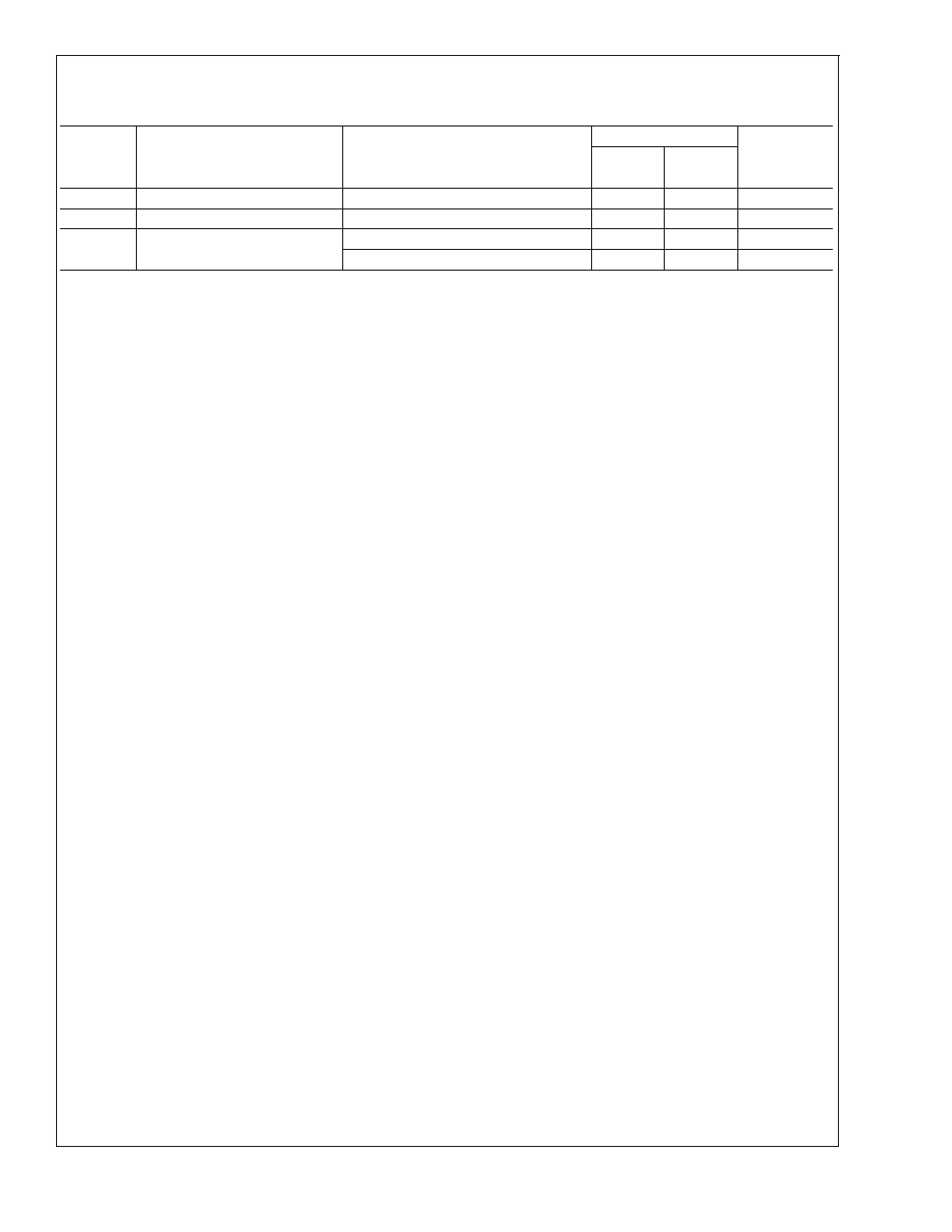
Electrical Characteristics V
DD
= 3.0V
(Notes 1, 5)
The following specifications apply for the circuit shown in Figure 2, unless otherwise specified. A
V
= 2.5, R
L
=
16
.Limits apply for T
A
= 25∞C.
Symbol
Parameter
Conditions
LM4924
Units
(Limits)
Typical
Limit
(Note 6)
(Note 7)
I
DD
Quiescent Power Supply Current V
IN
= 0V, I
O
= 0A, R
L
=
(Note 8)
1.5
1.9
mA (max)
I
SD
Shutdown Current
V
SHUTDOWN
= GND
0.1
1
µA (max)
V
OS
Output Offset Voltage
1
10
mV (max)
P
O
Output Power (Note 9)
f = 1kHz, per channel
OCL (Figure 2), THD+N = 1%
40
30
mW (min)
V
NO
Output Voltage Noise
20Hz to 20kHz, A-weighted, Figure 2
13
µV
RMS
THD
P
O
= 10mW
0.1
0.5
%
Crosstalk
Freq = 1kHz
45
35
dB (min)
PSRR
Power Supply Rejection Ratio
V
RIPPLE
= 200mV
P-P
sine wave
Freq = 100Hz, OCL
66
58
dB (min)
T
WAKE-UP
Wake-Up Time
1.5V
V
DD
3.6V, Fig 2
230
msec
V
IH
Control Logic High
1.5V
V
DD
3.6V
0.7V
DD
V (min)
V
IL
Control Logic Low
1.5V
V
DD
3.6V
0.3V
DD
V (max)
Mute
Attenuation
1V
PP
Reference, R
IN
= 20k, R
FB
= 50k
90
70
dB
Electrical Characteristics V
DD
= 1.8V
(Notes 1, 5)
The following specifications apply for the circuit shown in Figure 2, unless otherwise specified. A
V
= 2.5, R
L
= 16
.
Limits apply for T
A
= 25∞C.
Symbol
Parameter
Conditions
LM4924
Units
(Limits)
Typical
Limit
(Note 6)
(Note 7)
I
DD
Quiescent Power Supply Current
V
IN
= 0V, I
O
= 0A, R
L
=
(Note 8)
1.4
mA (max)
I
SD
Shutdown Current
V
SHUTDOWN
= GND
0.1
µA (max)
V
OS
Output Offset Voltage
1
mV (max)
P
O
Output Power (Note 9)
f = 1kHz
OCL Per channel, Fig. 2, Freq = 1kHz
THD+N = 1%
10
mW
V
NO
Output Voltage Noise
20Hz to 20kHz, A-weighted, Figure 2
10
µV
RMS
LM4924
www.national.com
4
Electrical Characteristics V
DD
= 1.8V
(Notes 1, 5) (Continued)
The following specifications apply for the circuit shown in Figure 2, unless otherwise specified. A
V
= 2.5, R
L
= 16
.
Limits apply for T
A
= 25∞C.
Symbol
Parameter
Conditions
LM4924
Units
(Limits)
Typical
Limit
(Note 6)
(Note 7)
THD
P
O
= 5mW
0.1
%
Crosstalk
Freq = 1kHz
45
dB (min)
PSRR
Power Supply Rejection Ratio
V
RIPPLE
= 200mV
P-P
sine wave
Freq = 100Hz, OCL
66
dB
Note 1: Absolute Maximum Ratings indicate limits beyond which damage to the device may occur. Operating Ratings indicate conditions for which the device is
functional, but do not guarantee specific performance limits. Electrical Characteristics state DC and AC electrical specifications under particular test conditions which
guarantee specific performance limits. This assumes that the device is within the Operating Ratings. Specifications are not guaranteed for parameters where no limit
is given, however, the typical value is a good indication of device performance.
Note 2: The maximum power dissipation is dictated by T
JMAX
,
JA
, and the ambient temperature T
A
and must be derated at elevated temperatures. The maximum
allowable power dissipation is P
DMAX
= (T
JMAX
- T
A
)/
JA
. For the LM4924, T
JMAX
= 150∞C. For the
JA
s, please see the Application Information section or the
Absolute Maximum Ratings section.
Note 3: Human body model, 100pF discharged through a 1.5k
resistor.
Note 4: Machine model, 220pF≠240pF discharged through all pins.
Note 5: All voltages are measured with respect to the ground (GND) pins unless otherwise specified.
Note 6: Typicals are measured at 25∞C and represent the parametric norm.
Note 7: Datasheet min/max specification limits are guaranteed by design, test, or statistical analysis.
Note 8: The quiescent power supply current depends on the offset voltage when a practical load is connected to the amplifier.
Note 9: Output power is measured at the device terminals.
LM4924
www.national.com
5