LM4934
3D Audio Sub-System with Stereo Speaker, OCL/SE
Stereo Headphone, Earpiece and Mono Line Level
Outputs
General Description
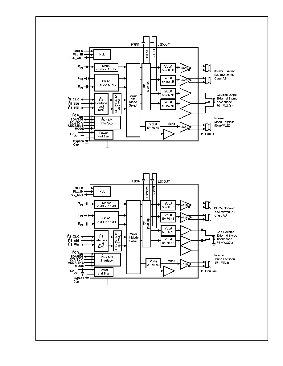
The LM4934 is an integrated audio sub-system designed for
stereo cell phone applications. Operating on a 3.3V supply, it
combines a stereo speaker amplifier delivering 520mW per
channel into an 8
load, a stereo headphone amplifier de-
livering 36mW per channel into a 32
load, a mono earpiece
amplifier delivering 55mW into a 32
load, and a line output
for an external powered handsfree speaker. It integrates the
audio amplifiers, volume control, mixer, power management
control, and National 3D enhancement all into a single pack-
age. In addition, the LM4934 routes and mixes the stereo
and mono inputs into multiple distinct output modes. The
LM4934 features an I2S serial interface for full range audio
and an I2C/SPI compatible interface for control.
Boomer audio power amplifiers are designed specifically to
provide high quality output power with a minimal amount of
external components.
Key Specifications
j
P
OUT
, Stereo BTL, 8
, 3.3V,
1% THD+N
520mW (typ)
j
P
OUT
HP, 32
, 3.3V, 1% THD+N
36mW (typ)
j
P
OUT
Mono Earpiece, 32
, 3.3V,
1% THD+N
55mW (typ)
j
Shutdown current
0.6µA (typ)
j
DAC SNR
95dB (typ)
Features
n
18-bit stereo DAC
n
Multiple distinct output modes
n
Stereo speaker amplifier
n
Stereo headphone amplifier
n
Mono earpiece amplifier
n
Mono Line Output for external handsfree carkit
n
Independent Left, Right, headphone and Mono speaker
volume controls
n
National 3D enhancement with programmable effect
level
n
I
2
C/SPI (selectable) compatible interface
n
Ultra low shutdown current
n
Click and Pop Suppression circuit
Applications
n
Cell Phones
n
PDAs
Boomer
Æ
is a registered trademark of National Semiconductor Corporation.
November 2005
LM4934
3D
Audio
Sub-System
with
Stereo
Speaker
,
OCL/SE
Stereo
Headphone,
Earpiece
and
Mono
Line
Level
Outputs
© 2005 National Semiconductor Corporation
DS201669
www.national.com
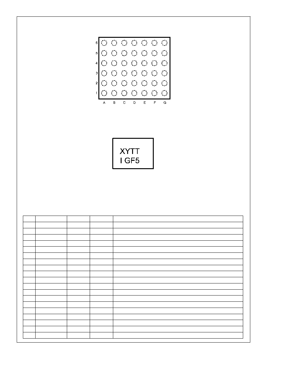
Connection Diagrams
42-Bump Microfil
20166958
Top View (Bump Side Down)
Order Number LM4934WL
See NS Package Number WLA42
Top Marking Drawing
201669K6
Top View
XY -- 2 Digit Date Code
TT -- Traceability
GF5 -- LM4934
I -- Pin 1 Marking
Pin Descriptions
PIN
PIN NAME
D/A
I/O
DESCRIPTION
A1
DGND
D
P
DIGITAL GROUND
A2
MCLK
D
I
MASTER CLOCK
A3
I2S_WS
D
I/O
I2S WORD SELECT
A4
GPIO
D
O
TEST PIN (MUST BE LEFT FLOATING)
A5
ADDR/ENB
D
I
I2C_ADDR OR SPI_ENB DEPENDING ON I2C or SPI MODE SELECT
A6
DVDD
D
P
DIGITAL SUPPLY VOLTAGE
B1
PLLVDD
D
P
PLL SUPPLY VOLTAGE
B2
I2S_SDI
D
I
I2S SERIAL DATA INPUT
B3
I2S_CLK
D
I/O
I2S CLOCK SIGNAL
B4
MODE
D
I
SELECTS BETWEEN SPI AND I2C CONTROL INTERFACE
B5
I2C_VDD
D
P
I2C SUPPLY VOLTAGE
B6
VDDIO
D
P
I/O SUPPLY VOLTAGE
C1
PLL_IN
D
I
PLL FILTER INPUT
C2
PLL_OUT
D
O
PLL FILTER OUTPUT
C3
PLLGND
D
P
PLL GND
C4
SDA/SDI
D
I/O
I2C SDA OR SPI SDI
C5
SCL/SCK
D
I
I2C_SCL OR SPI_SCK
C6
AVDD
A
P
ANALOG SUPPLY VOLTAGE
D1
AGND
A
P
ANALOG GROUND
LM4934
www.national.com
3
Absolute Maximum Ratings
(Notes 1, 2)
If Military/Aerospace specified devices are required,
please contact the National Semiconductor Sales Office/
Distributors for availability and specifications.
Analog Supply Voltage
6.0V
Digital Supply Voltage
6.0V
Storage Temperature
-65∞C to +150∞C
Input Voltage
-0.3V to V
DD
+0.3V
Power Dissipation (Note 3)
Internally Limited
ESD Susceptibility (Note 4)
2000V
ESD Susceptibility(Note 5)
200V
Junction Temperature
150∞C
Thermal Resistance
JA
(WLA42)
61∞C/W
See AN-1279
Operating Ratings
Temperature Range
T
MIN
T
A
T
MAX
-40∞C
T
A
+85∞C
Supply Voltage
2.7V
AV
DD
5.5V
2.7V
DV
DD
4.0V
2.4V
I
2
CV
DD
4.0V
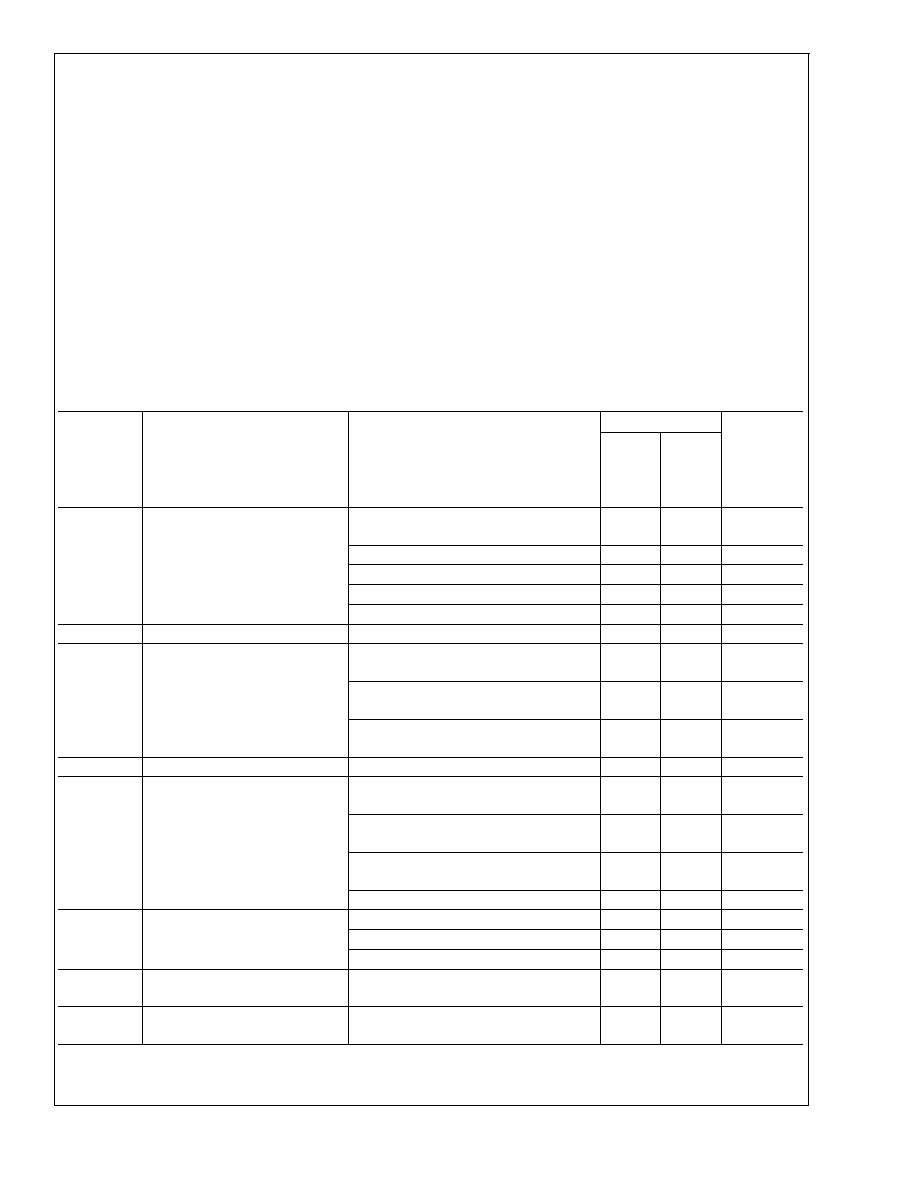
Audio Amplifier Electrical Characteristics AV
DD
= 3.0V, DV
DD
= 3.0V
(Notes 1,
2)
The following specifications apply for the circuit shown in Figure 1 with all programmable gain set at 0dB, unless otherwise
specified. Limits apply for T
A
= 25∞C.
Symbol
Parameter
Conditions
LM4934
Units
(Limits)
Typical
(Note 6)
Limits
(Notes
7, 8)
I
DD
Supply Current
V
IN
= 0, No Load
All Amps On + DAC, OCL
18.5
26.5
mA (max)
Headphone Mode Only, OCL
5.6
8
mA (max)
Stereo Speaker Mode Only
12
19.5
mA (max)
Mono Earpiece Mode Only
5.9
8
mA (max)
DAC Off, All Amps On, OCL
14.6
22
mA (max)
I
SD
Shutdown Current
0.6
2
µA (max)
P
O
Output Power
Speaker; THD = 1%;
f = 1kHz, 8
BTL
420
370
mW (min)
Headphone; THD = 1%;
f = 1kHz, 32
SE
27
24
mW (min)
Earpiece; THD = 1%;
f = 1kHz, 32
BTL
45
40
mW (min)
V
FS DAC
Full Scale DAC Output
2.4
Vpp
THD+N
Total Harmonic Distortion
Speaker; P
O
= 200mW;
f = 1kHz, 8
BTL
0.04
%
Headphone; P
O
= 10mW;
f = 1kHz, 32
SE
0.01
%
Earpiece; P
O
= 20mW;
f = 1kHz, 32
BTL
0.04
%
Line Out; V
O
= 1Vrms; f = 1kHz, 10k
SE
0.004
%
V
OS
Offset Voltage
Speaker
8
55
mV (max)
Earpiece
8
50
mV (max)
HP (OCL)
8
40
mV
O
Output Noise
A = weighted; 0dB gain;
See Table 1
Table 1
PSRR
Power Supply Rejection Ratio
f = 217Hz; V
ripple
= 200mV
P-P
C
B
= 2.2µF; See Table 2
Table 2
LM4934
www.national.com
5