 | –≠–ª–µ–∫—Ç—Ä–æ–Ω–Ω—ã–π –∫–æ–º–ø–æ–Ω–µ–Ω—Ç: LM4936MH | –°–∫–∞—á–∞—Ç—å:  PDF PDF  ZIP ZIP |
LM4936
Stereo 2W Audio Power Amplifiers with Volume Control
and Selectable Control Interface (SPI or I
2
C)
General Description
The LM4936 is a monolithic integrated circuit that provides
volume control, and stereo bridged audio power amplifiers
capable of producing 2W into 4
(Note 1) with less than 1%
THD or 2.2W into 3
(Note 2) with less than 1% THD.
Boomer
Æ
audio integrated circuits were designed specifically
to provide high quality audio while requiring a minimum
amount of external components. The LM4936 incorporates a
SPI or I
2
C Control Interface that runs the volume control,
stereo bridged audio power amplifiers and a selectable gain
or bass boost. All of the LM4936's features (i.e. SD, Mode,
Mute, Gain Sel) make it optimally suited for multimedia
monitors, portable radios, desktop, and portable computer
applications.
The LM4936 features an externally controlled, low-power
consumption shutdown mode, and both a power amplifier
and headphone mute for maximum system flexibility and
performance.
Note 1: When properly mounted to the circuit board, LM4936MH will deliver
2W into 4
. See Application Information section Exposed-DAP package
PCB Mounting Considerations for more information.
Note 2: An LM4936MH that has been properly mounted to the circuit board
and forced-air cooled will deliver 2.2W into 3
.
Key Specifications
n
P
O
at 1% THD+N
n
into 3
2.2W (typ)
n
into 4
2.0W (typ)
n
into 8
1.25W (typ)
n
Single-ended mode - THD+N at 90mW into 32
1%(typ)
n
Shutdown current
0.7µA (typ)
Features
n
Selectable SPI or I
2
C Control Interface
n
System Beep Detect
n
Stereo switchable bridged/single-ended power amplifiers
n
Selectable internal/external gain and bass boost
n
"Click and pop" suppression circuitry
n
Thermal shutdown protection circuitry
n
Headphone Sense
Applications
n
Portable and Desktop Computers
n
Multimedia Monitors
n
Portable Radios, PDAs, and Portable TVs
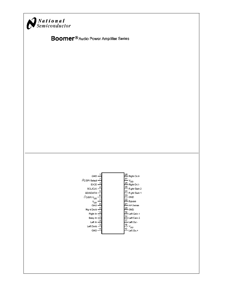
Connection Diagram
TSSOP Package
20117802
Top View
Order Number LM4936MH
See NS Package Number MXA28A for Exposed-DAP TSSOP
Boomer
Æ
is a registered trademark of NationalSemiconductor Corporation.
April 2005
LM4936
Stereo
2W
Audio
Power
Amplifiers
with
V
olume
Control
and
Selectable
Control
Interface
(SPI
or
I
2
C)
© 2005 National Semiconductor Corporation
DS201178
www.national.com
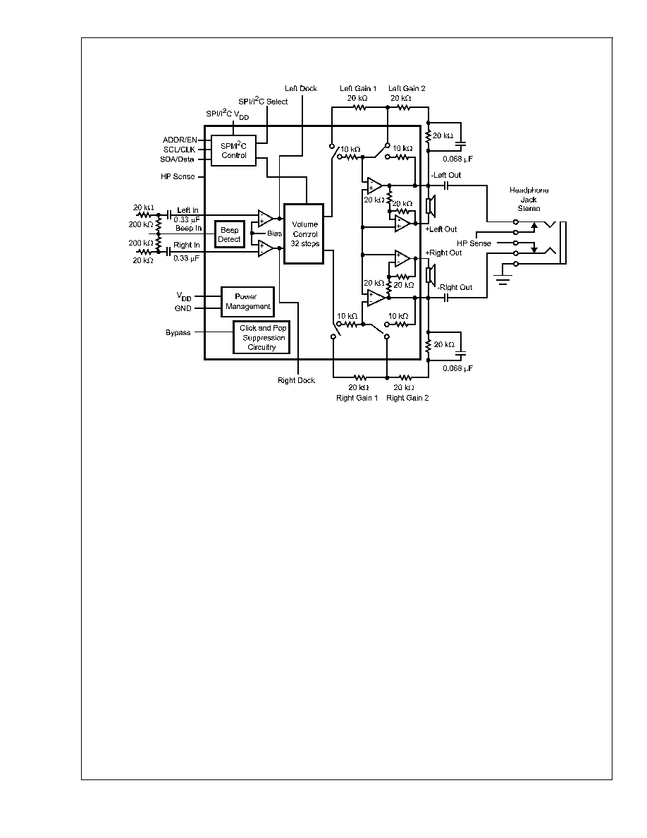
Block Diagram
20117801
FIGURE 1. LM4936 Block Diagram
LM4936
www.national.com
2
Absolute Maximum Ratings
(Note 10)
If Military/Aerospace specified devices are required,
please contact the National Semiconductor Sales Office/
Distributors for availability and specifications.
Supply Voltage
6.0V
Storage Temperature
-65∞C to +150∞C
Input Voltage
-0.3V to V
DD
+0.3V
Power Dissipation (Note 11)
Internally limited
ESD Susceptibility (Note 12)
2000V
ESD Susceptibility (Note 13)
200V
Junction Temperature
150∞C
Soldering Information
Small Outline Package
Vapor Phase (60 sec.)
215∞C
Infrared (15 sec.)
220∞C
See AN-450 "Surface Mounting and their Effects on
Product Reliability" for other methods of soldering surface
mount devices.
JC
(typ) - MXA28A
2∞C/W
JA
(typ) - MXA28A (exposed DAP) (Note 4)
41∞C/W
JA
(typ) - MXA28A (exposed DAP) (Note 3)
54∞C/W
JA
(typ) - MXA28A (exposed DAP) (Note 5)
59∞C/W
JA
(typ) - MXA28A (exposed DAP) (Note 6)
93∞C/W
Operating Ratings
Temperature Range
T
MIN
T
A
T
MAX
-40∞C
TA 85∞C
Supply Voltage (Note 17)
2.7V
V
DD
5.5V
I
2
C/SPI V
DD
V
DD
2.4V
I
2
C/SPI V
DD
5.5V
Electrical Characteristics for Entire IC
(Notes 7, 10)
The following specifications apply for V
DD
= 5V unless otherwise noted. Limits apply for T
A
= 25∞C.
Symbol
Parameter
Conditions
LM4936
Units
(Limits)
Typical
(Note 14)
Limit
(Note 15)
V
DD
Supply Voltage
2.7
V (min)
5.5
V (max)
I
DD
Quiescent Power Supply Current
V
IN
= 0V, I
O
= 0A
10
25
mA (max)
I
SD
Shutdown Current
V
shutdown
= V
DD
0.7
2.0
µA (max)
V
IH
Headphone Sense High Input Voltage
4
V (min)
V
IL
Headphone Sense Low Input Voltage
0.8
V (max)
Electrical Characteristics for Volume Control
(Notes 7, 10)
The following specifications apply for V
DD
= 5V. Limits apply for T
A
= 25∞C.
Symbol
Parameter
Conditions
LM4936
Units
(Limits)
Typical
(Note 14)
Limit
(Note 15)
C
RANGE
Volume Control Range
Maximum gain setting
0
±
0.75
dB (max)
Minimum gain setting
-91
-75
dB (min)
A
Ch-Ch
Channel to Channel Gain Mismatch
f
IN
= 1kHz
0.35
dB
A
M
Mute Attenuation
Mute Mode
-78
dB (min)
Electrical Characteristics for Control Interface
(Notes 7, 10)
The following specifications apply for V
DD
= 5V, V
DD
= 3V and 2.4V
I
2
C/SPI V
DD
5.5V. Limits apply for T
A
= 25∞C.
Symbol
Parameter
Conditions
LM4936
Units
(Limits)
Typical
(Note 14)
Limit
(Note 15)
t
1
SCL period
2.5
µs (min)
t
2
SDA Set-up Time
100
ns (min)
t
3
SDA Stable Time
0
ns (min)
t
4
Start Condition Time
100
ns (min)
t
5
Stop Condition Time
100
ns (min)
LM4936
www.national.com
3
Electrical Characteristics for Control Interface
(Notes 7, 10) (Continued)
The following specifications apply for V
DD
= 5V, V
DD
= 3V and 2.4V
I
2
C/SPI V
DD
5.5V. Limits apply for T
A
= 25∞C.
Symbol
Parameter
Conditions
LM4936
Units
(Limits)
Typical
(Note 14)
Limit
(Note 15)
V
IH
Digital Input High Voltage
0.7 X
I
2
C/SPIV
DD
V (min)
V
IL
Digital Input Low Voltage
0.3 X
I
2
C/SPIV
DD
V (max)
t
ES
SPI ENABLE Setup Time
50
ns (min)
t
EH
SPI ENABLE Hold Time
50
ns (min)
t
EL
SPI ENABLE High Time
50
ns (min)
t
DS
SPI DATA Setup Time
50
ns (min)
t
DH
SPI DATA HOLD Time
50
ns (min)
t
CS
SPI CLOCK Setup Time
50
ns (min)
t
CH
SPI CLOCK High Pulse Width
100
ns (min)
t
CL
SPI CLOCK Low Pulse Width
100
ns (min)
f
CLK
SPI CLOCK Frequency
5
MHz (max)
Electrical Characteristics for Single-Ended Mode Operation
(Notes 7, 10)
The following specifications apply for V
DD
= 5V. Limits apply for T
A
= 25∞C.
Symbol
Parameter
Conditions
LM4936
Units
(Limits)
Typical
(Note 14)
Limit
(Note 15)
P
O
Output Power
THD = 1%; f = 1kHz; R
L
= 32
90
mW
THD = 10%; f = 1 kHz; R
L
= 32
110
mW
THD+N
Total Harmonic Distortion+Noise
P
OUT
= 20mW, f = 1kHz, R
L
= 32
,
A
VD
= 1, 80kHz BW
0.02
%
PSRR
Power Supply Rejection Ratio
C
B
= 1µF, f = 120Hz,
Input Terminated
V
RIPPLE
= 200mVp-p
57
dB
N
OUT
Output Noise
A-Wtd Filter
18
µV
X
talk
Channel Separation (Note 17)
f = 1kHz, C
B
= 1µF
63
dB
Electrical Characteristics for Bridged Mode Operation
(Notes 7, 10)
The following specifications apply for V
DD
= 5V, unless otherwise noted. Limits apply for T
A
= 25∞C.
Symbol
Parameter
Conditions
LM4936
Units
(Limits)
Typical
(Note 14)
Limit
(Note 15)
V
OS
Output Offset Voltage
V
IN
= 0V, No Load
10
50
mV (max)
P
O
Output Power
THD + N = 1%; f = 1kHz; R
L
= 3
(Note 8)
2.2
W
THD + N = 1%; f = 1kHz; R
L
= 4
(Note 9)
2
W
THD+N = 1% (max); f = 1kHz;
R
L
= 8
1.25
1.0
W (min)
THD+N = 10%; f = 1kHz; R
L
= 8
1.6
W
THD+N
Total Harmonic Distortion+Noise
P
O
= 0.4W, f = 1kHz
R
L
= 8
, A
VD
= 2, 80kHz BW
0.06
%
PSRR
Power Supply Rejection Ratio
C
B
= 1µF, f = 120Hz,
Input Terminated
V
RIPPLE
= 200mVp-p; R
L
= 8
55
dB
LM4936
www.national.com
4
Electrical Characteristics for Bridged Mode Operation
(Notes 7, 10) (Continued)
The following specifications apply for V
DD
= 5V, unless otherwise noted. Limits apply for T
A
= 25∞C.
Symbol
Parameter
Conditions
LM4936
Units
(Limits)
Typical
(Note 14)
Limit
(Note 15)
N
OUT
Output Noise
A-Wtd Filter
36
µV
X
talk
Channel Separation (Note 17)
f = 1kHz, C
B
= 1µF
63
dB
Note 3: The
JA
given is for an MXA28A package whose exposed-DAP is soldered to an exposed 2in
2
piece of 1 ounce printed circuit board copper.
Note 4: The
JA
given is for an MXA28A package whose exposed-DAP is soldered to a 2in
2
piece of 1 ounce printed circuit board copper on a bottom side layer
through 21 8mil vias.
Note 5: The
JA
given is for an MXA28A package whose exposed-DAP is soldered to an exposed 1in
2
piece of 1 ounce printed circuit board copper.
Note 6: The
JA
given is for an MXA28A package whose exposed-DAP is not soldered to any copper.
Note 7: All voltages are measured with respect to the ground pins, unless otherwise specified. All specifications are tested using the typical application as shown
in Figure 1.
Note 8: When driving 3
loads from a 5V supply the LM4936MH must be mounted to the circuit board and forced-air cooled. The demo board shown in the
datasheet has planes for heat sinking. The top layer plane is 1.05 in
2
(675mm
2
), the inner two layers each have a 1.03 in
2
(667mm
2
) plane and the bottom layer
has a 3.32 in
2
(2143mm
2
) plane. The planes are electrically GND and interconnected through six 15 mil vias directly under the package and eight 28 mil vias in
various locations.
Note 9: When driving 4
loads from a 5V supply the LM4936MH must be mounted to the circuit board. The demo board shown in the datasheet has planes for heat
sinking. The top layer plane is 1.05 in
2
(675mm
2
), the inner two layers each have a 1.03 in
2
(667mm
2
) plane and the bottom layer has a 3.32 in
2
(2143mm
2
) plane.
The planes are electrically GND and interconnected through six 15 mil vias directly under the package and eight 28 mil vias in various locations.
Note 10: Absolute Maximum Ratings indicate limits beyond which damage to the device may occur. Operating Ratings indicate conditions for which the device is
functional, but do not guarantee specific performance limits. Electrical Characteristics state DC and AC electrical specifications under particular test conditions which
guarantee specific performance limits. This assumes that the device is within the Operating Ratings. Specifications are not guaranteed for parameters where no limit
is given, however, the typical value is a good indication of device performance.
Note 11: The maximum power dissipation must be derated at elevated temperatures and is dictated by T
JMAX
,
JA
, and the ambient temperature T
A
. The maximum
allowable power dissipation is P
DMAX
= (T
JMAX
- T
A
)/
JA
. For the LM4936, T
JMAX
= 150∞C, and the typical junction-to-ambient thermal resistance for each package
can be found in the Absolute Maximum Ratings section above.
Note 12: Human body model, 100pF discharged through a 1.5k
resistor.
Note 13: Machine Model, 220pF ≠ 240pF discharged through all pins.
Note 14: Typicals are measured at 25∞C and represent the parametric norm.
Note 15: Limits are guaranteed to National's AOQL ( Average Outgoing Quality Level). Datasheet min/max specification limits are guaranteed by design, test, or
statistical analysis.
Note 16: I
2
C/SPI V
DD
must not be larger than V
DD
at any time or damage to the IC may occur. During power up and power down, I
2
C/SPI V
DD
must remain equal
to V
DD
or lower.
Note 17: PCB design will affect Crosstalk performance.
LM4936
www.national.com
5