 | –≠–ª–µ–∫—Ç—Ä–æ–Ω–Ω—ã–π –∫–æ–º–ø–æ–Ω–µ–Ω—Ç: LM494IN | –°–∫–∞—á–∞—Ç—å:  PDF PDF  ZIP ZIP |
TL H 10056
LM494
Pulse
Width
Modulated
Control
Circuit
June 1989
LM494
Pulse Width Modulated Control Circuit
General Description
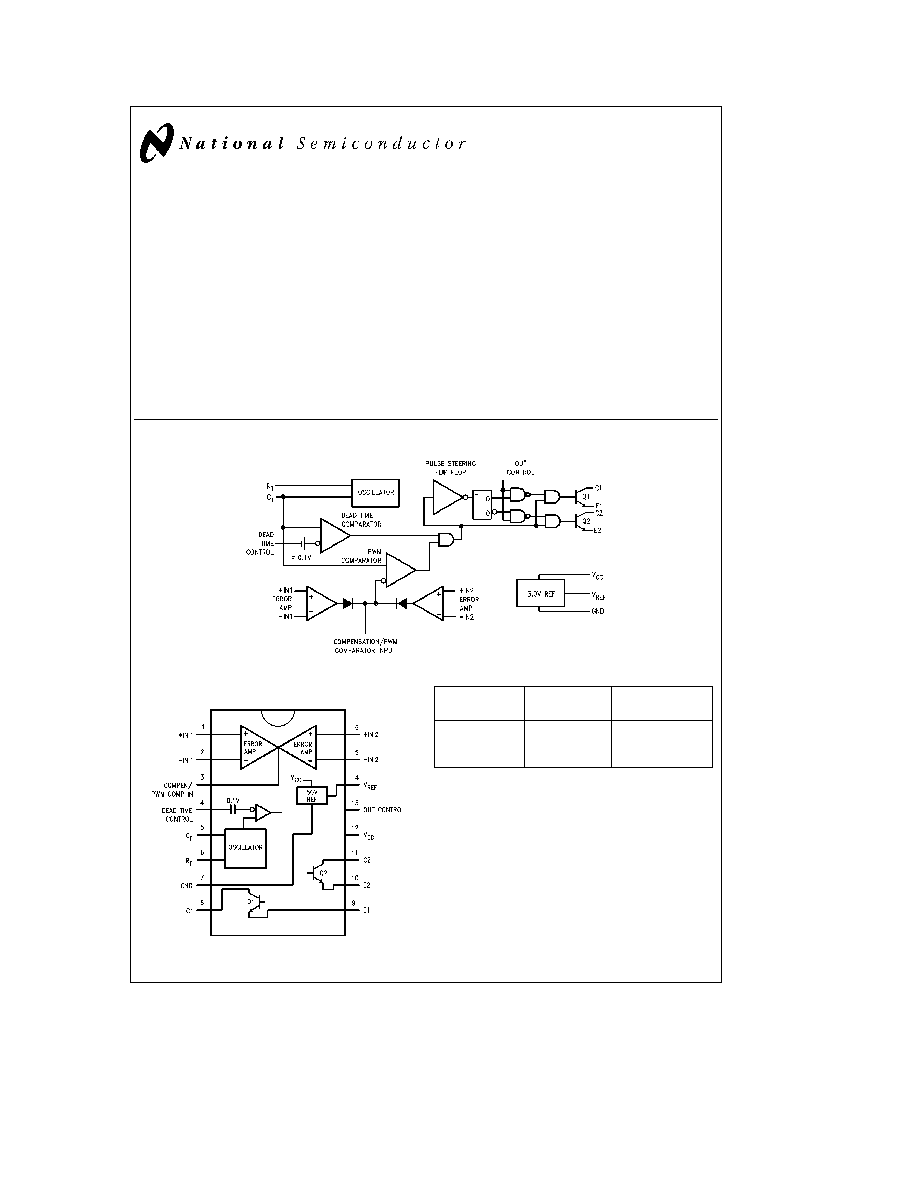
The LM494 is a monolithic integrated circuit which includes
all the necessary building blocks for the design of pulse
width modulated (PWM) switching power supplies including
push-pull bridge and series configurations The device can
operate at switching frequencies between 1 0 kHz and
300 kHz and output voltages up to 40V The operating tem-
perature range specified for the LM494C is 0 C to 70 C and
for the LM494V is
b
40 C to
a
85 C
Features
Y
Uncommitted output transistors capable of 200 mA
source or sink
Y
On-chip error amplifiers
Y
On-chip 5 0V reference
Y
Internal protection from double pulsing of outputs with
narrow pulse widths or with supply voltages below
specified limits
Y
Dead time control comparator
Y
Output control selects single ended or push-pull opera-
tion
Y
Easily synchronized (slaved) to other circuits
Block Diagram
TL H 10056 ≠ 2
Connection Diagram
16-Lead DIP
TL H 10056 ≠ 1
Top View
Ordering Information
Device
Package
Package
Code
Code
Description
LM494IN
N16A
Molded DIP
LM494CJ
J16A
Ceramic DIP
LM494CN
N16A
Molded DIP
C1995 National Semiconductor Corporation
RRD-B30M115 Printed in U S A
Absolute Maximum Ratings
If Military Aerospace specified devices are required
please contact the National Semiconductor Sales
Office Distributors for availability and specifications
Storage Temperature Range
Ceramic DIP
b
65 C to
a
175 C
Molded DIP
b
65 C to
a
150 C
Operating Temperature Range
Industrial (LM494I)
b
40 C to
a
85 C
Commercial (LM494C)
0 C to
a
70 C
Lead Temperature
Ceramic DIP (Soldering 60 sec )
300 C
Molded DIP (Soldering 10 sec )
265 C
Internal Power Dissipation (Notes 1 2)
16L-Ceramic DIP
1 50W
16L-Molded DIP
1 04W
Supply Voltage
42V
Voltage from Any Lead to Ground
(except Lead 8 and Lead 11)
V
CC
a
0 3V
Output Collector Voltage
42V
Peak Collector Current
(I
C1
and I
C2
)
250 mA
ESD Susceptibility
(to be determined)
Recommended Operating
Conditions
Power Supply Voltage (V
CC
)
7 0V to 40V
Voltage on Any Lead
except Leads 8 and 11
(Referenced to Ground) (V
I
)
b
0 3V to V
CC
a
0 3V
Output Voltage Collector (V
C1
V
C2
)
b
0 3V to 40V
Output Collector Current (I
C1
I
C2
)
200 mA
Timing Capacitor (C
T
)
470 pF to 10 mF
Timing Resistor (R
T
)
1 8 kX to 500 kX
Oscillator Frequency (f
OSC
)
1 0 kHz to 300 kHz
LM494
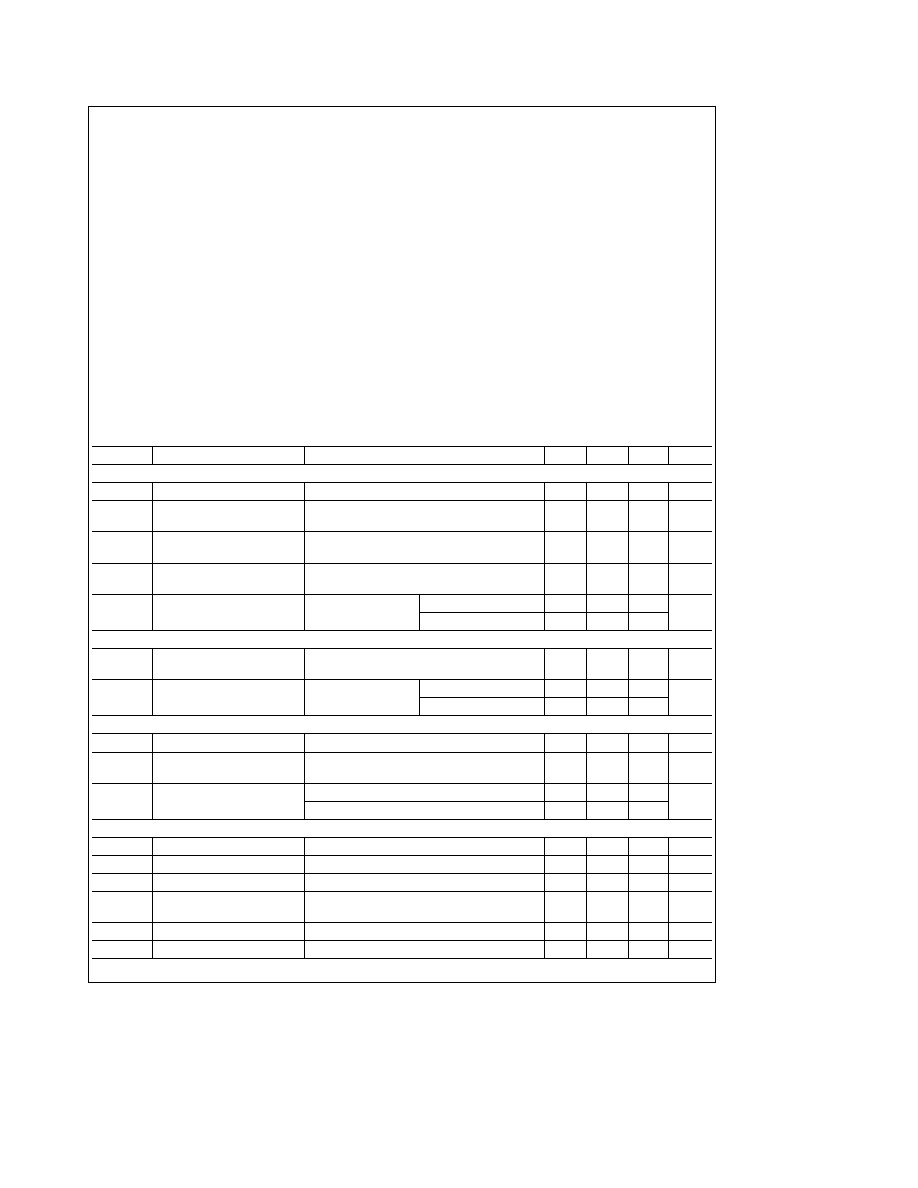
Electrical Characteristics
T
A
e
0 C to
a
70 C for the LM494C T
A
e b
40 C to
a
85 C for the LM494I V
CC
e
15V f
OSC
e
10 kHz unless otherwise specified
Symbol
Parameter
Conditions
Min
Typ
Max
Units
REFERENCE SECTION
V
REF
Reference Voltage (Note 3)
I
REF
e
1 0 mA
4 75
5 0
5 25
V
Reg
LINE
Line Regulation of
7 0V
s
V
CC
s
40V
2 0
25
mV
Reference Voltage
TCV
REF
Temperature Coefficient of
0 C
s
T
A
s
70 C
0 01
0 03
% C
Reference Voltage
Reg
LOAD
Load Regulation of
1 0 mA
s
I
REF
s
10 mA
1 0
15
mV
Reference Voltage
I
OS
Output Short Circuit Current
V
REF
e
0V
0 C
s
T
A
s
a
70 C
10
35
50
mA
b
40 C
s
T
A
s
a
85 C
35
OSCILLATOR SECTION
f
OSC
Oscillator Frequency
C
T
e
0 01 mF
10
kHz
(Figure 10)
R
T
e
12 kX
D
f
OSC
Oscillator Frequency Change
C
T
e
0 01 mF
0 C
s
T
A
s
a
70 C
2 0
%
R
T
e
12 kX
b
40 C
s
T
A
s
a
85 C
2 0
DEAD TIME CONTROL SECTION
I
IB (DT)
Input Bias Current
V
CC
e
15V 0V
s
V
4
s
5 25V
b
2 0
b
10
m
A
DC
(Max)
Maximum Duty Cycle
V
CC
e
15V Lead 4
e
0V
45
%
Each Output
Output Control
e
V
REF
V
TH(in)
Input Threshold Voltage
Zero Duty Cycle
3 0
3 3
V
Maximum Duty Cycle
0
ERROR AMPLIFIER SECTIONS
V
IO
Input Offset Voltage
V
3
e
2 5V
V
3
e
2 5V
2 0
10
mV
I
IO
Input Offset Current
V
3
e
2 5V
25
250
nA
I
IB
Input Bias Current
V
3
e
2 5V
0 2
1 0
m
A
V
ICR
Input Common Mode
7 0V
s
V
CC
s
40V
b
0 3
V
CC
V
Voltage Range
A
VS
Large Signal Voltage Gain
0 5V
s
V
3
s
3 5V
60
74
dB
BW
Bandwidth
650
kHz
2
LM494
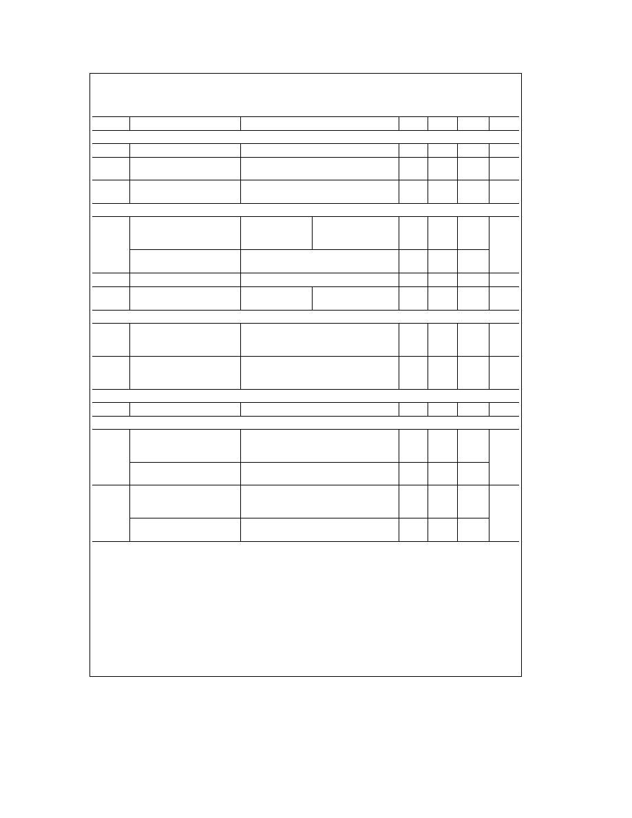
Electrical Characteristics
T
A
e
0 C to
a
70 C for the LM494C T
A
e b
40 C to
a
85 C for the LM494I
V
CC
e
15V f
OSC
e
10 kHz unless otherwise specified (Continued)
Symbol
Parameter
Conditions
Min
Typ
Max
Units
PWM COMPARATOR SECTION
(Figure 9)
V
THI
Inhibit Threshold Voltage
Zero Duty Cycle
4 0
4 5
V
I
O
b
Output Sink Current
0 5V
s
V
3
s
3 5V
b
0 2
b
0 6
mA
(Note 4)
I
O
a
Output Source Current
0 5V
s
V
3
s
3 5V
2 0
mA
(Note 4)
OUTPUT SECTION
V
CE(sat)
Output Saturation
V
E
e
0V
0 C
s
T
A
s
a
70 C
Voltage Common Emitter
I
C
e
200 mA
b
40 C
s
T
A
s
a
85 C
1 1
1 3
Configuration
(Figure 3)
V
Emitter Follower
V
C
e
15V I
E
e
200 mA
1 5
2 5
Configuration
(Figure 4)
I
C(off)
Collector Off-State Current
V
CC
e
40V V
CE
e
40V
2 0
100
m
A
I
E(off)
Emitter Off-State Current
V
CC
e
V
C
e
40V
0 C
s
T
A
s
a
70 C
b
100
m
A
V
E
e
0
b
40 C
s
T
A
s
a
85 C
OUTPUT CONTROL
(Figure 6)
V
OCL
Output Control Voltage
Required for Single Ended or
0 4
V
Parallel Output Operation
V
OCH
Output Control Voltage
Required for Push-Pull
2 4
V
Operation
TOTAL DEVICE
I
CC
Standby Power Supply Current
6 0
10
mA
OUTPUT AC CHARACTERISTICS
Use Recommended Operating Conditions with T
A
e
25 C
t
r
Rise Time of Output Voltage
Common Emitter Configuration
100
200
(Figure 3)
ns
Emitter Follower Configuration
100
200
(Figure 4)
t
f
Fall Time of Output Voltage
Common Emitter Configuration
25
100
(Figure 3)
ns
Emitter Follower Configuration
40
100
(Figure 4)
Note 1
T
J Max
e
150 C for the Molded DIP and 175 C for the Ceramic DIP
Note 2
Ratings apply to ambient temperature at 25 C Above this temperature derate the 16L-Ceramic DIP at 10 mW C and the 16L-Molded DIP at 8 3 mW C
Note 3
Selected devices with tightened tolerance reference voltage available
Note 4
These limits apply when the voltage measured at Lead 3 is within the range specified
3
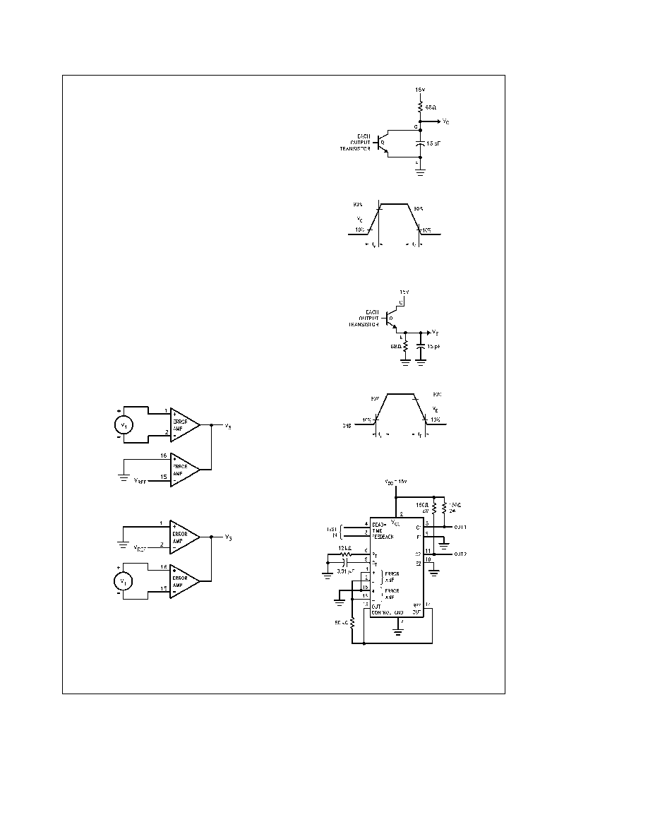
Functional Description
The basic oscillator (switching) frequency is controlled by an
external resistor (R
T
) and capacitor (C
T
) The relationship
between the values of R
T
C
T
and frequency is shown in
Figure 10
The level of the sawtooth wave form is compared with an
error voltage by the pulse width modulated comparator The
output of the PWM Comparator directs the pulse steering
flip-flop and the output control logic
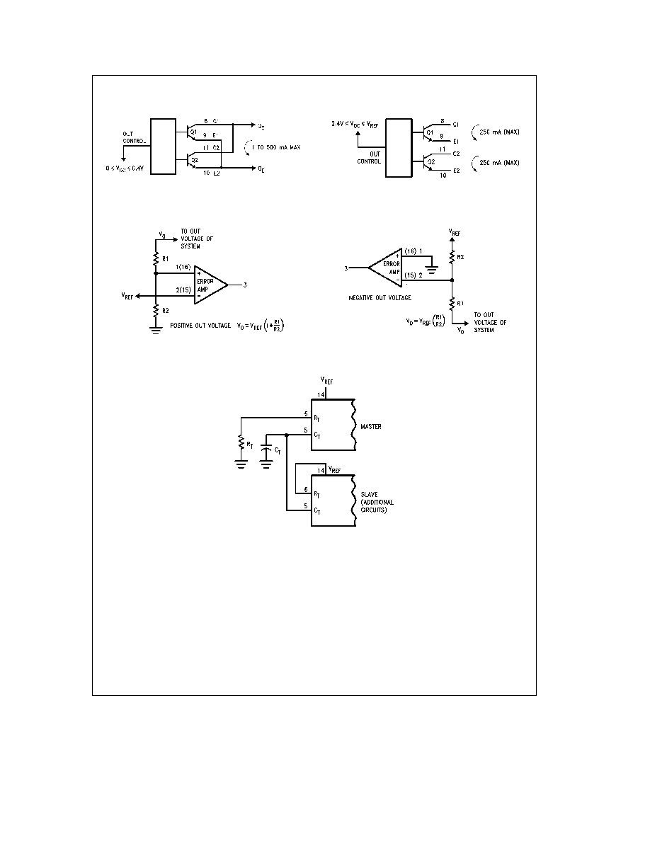
The error voltage is generated by the error amplifier The
error amplifier boosts the voltage difference between the
output and the 5 0V internal reference See
Figure 7 for
error amp sensing techniques The second error amp is typi-
cally used to implement current-limiting
The output control logic selects either push-pull or single-
ended operation of the output transistors (see
Figure 6 )
The dead time control prevents on-state overlap of the out-
put transistors as can be seen in
Figure 5 The dead time is
approximately 3 0% or 5 0% of the total period if the dead
time control is grounded This dead time can be increased
by connecting the dead time control to a voltage up to 5 0V
The frequency response of the error amps
(Figure 11) can
be modified by using external resistors and capacitors
These components are typically connected between the
compensation terminal and the inverting input of the error
amps
The switching frequency of two or more LM494 circuits can
be synchronized The timing capacitor C
T
is connected as
shown in
Figure 8 Charging current is provided by the mas-
ter circuit Discharging is through all the circuits slaved to
the master R
T
is required only for the master circuit
Test Circuits
TL H 10056 ≠ 3
FIGURE 1 Error Amplifier Test Circuit
TL H 10056 ≠ 4
FIGURE 2 Current Limit Sense
Amplifier Test Circuit
TL H 10056 ≠ 5
TL H 10056 ≠ 6
FIGURE 3 Common Emitter Configuration
Test Circuit and Waveform
TL H 10056 ≠ 7
TL H 10056 ≠ 8
FIGURE 4 Emitter Follower Configuration
Test Circuit and Waveform
TL H 10056 ≠ 9
FIGURE 5 Dead Time and Feedback
Control Test Circuit
4
Typical Applications
TL H 10056 ≠ 10
TL H 10056 ≠ 11
FIGURE 6 Output Connections for Single Ended
and Push-Pull Configurations
TL H 10056 ≠ 12
TL H 10056 ≠ 13
FIGURE 7 Error Amplifier Sensing Techniques
TL H 10056 ≠ 14
FIGURE 8 Slaving Two or More Control Circuits
5