 | –≠–ª–µ–∫—Ç—Ä–æ–Ω–Ω—ã–π –∫–æ–º–ø–æ–Ω–µ–Ω—Ç: LM4950 | –°–∫–∞—á–∞—Ç—å:  PDF PDF  ZIP ZIP |
LM4950
7.5W Mono-BTL or 3.1W Stereo Audio Power Amplifier
General Description
The LM4950 is a dual audio power amplifier primarily de-
signed for demanding applications in flat panel monitors and
TV's. It is capable of delivering 3.1 watts per channel to a 4
single-ended load with less than 1% THD+N or 7.5 watts
mono BTL to an 8
load, with less than 10% THD+N from a
12V
DC
power supply.
Boomer audio power amplifiers were designed specifically to
provide high quality output power with a minimal amount of
external components. The LM4950 does not require boot-
strap capacitors or snubber circuits. Therefore, it is ideally
suited for display applications requiring high power and mini-
mal size.
The LM4950 features a low-power consumption active-low
shutdown mode. Additionally, the LM4950 features an inter-
nal thermal shutdown protection mechanism along with short
circuit protection.
The LM4950 contains advanced pop & click circuitry that
eliminates noises which would otherwise occur during
turn-on and turn-off transitions.
The LM4950 is a unity-gain stable and can be configured by
external gain-setting resistors.
Key Specifications
j
Quiscent Power Supply Current
16mA (typ)
j
P
OUT
(SE)
V
DD
= 12V, R
L
= 4
, 1% THD+N
3.1W (typ)
j
P
OUT
(BTL)
V
DD
= 12V, R
L
= 8
, 10% THD+N
7.5W (typ)
j
Shutdown current
40µA (typ)
Features
n
Pop & click circuitry eliminates noise during turn-on and
turn-off transitions
n
Low current, active-low shutdown mode
n
Low quiescent current
n
Stereo 3.1W output, R
L
= 4
n
Mono 7.5W BTL output, R
L
= 8
n
Short circuit protection
n
Unity-gain stable
n
External gain configuration capability
Applications
n
Flat Panel Monitors
n
Flat panel TV's
n
Computer Sound Cards
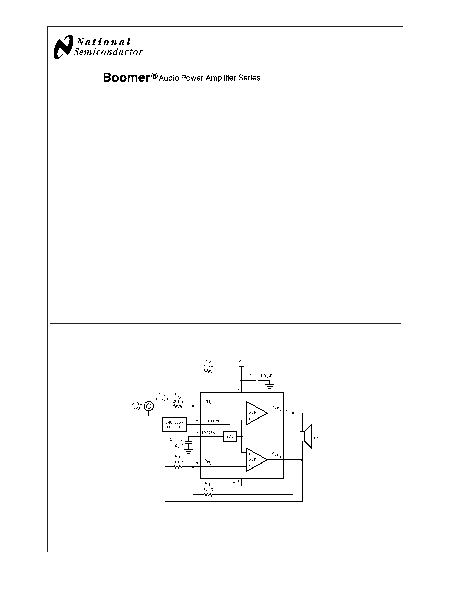
Typical Application
Boomer
Æ
is a registered trademark of National Semiconductor Corporation.
20047078
FIGURE 1. Typical Bridge-Tied-Load (BTL) Audio Amplifier Application Circuit
August 2004
LM4950
7.5W
Mono-BTL
or
3.1W
Stereo
Audio
Power
Amplifier
© 2004 National Semiconductor Corporation
DS200470
www.national.com
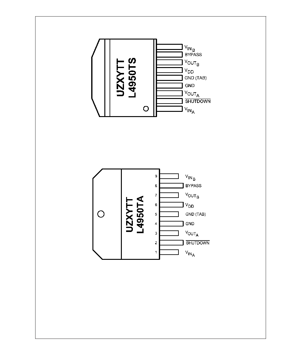
Connection Diagrams
Plastic Package, TO-263
20047070
Top View
U = Wafer Fab Code
Z = Assembly Plant Code
XY = Date Code
TT = Die Traceability
Order Number LM4950TS
See NS Package Number TS9A
Plastic Package, TO-220
20047071
Top View
U = Wafer Fab Code
Z = Assembly Plant Code
XY = Date Code
TT = Die Traceability
Order Number LM4950TA
See NS Package Number TA09A
LM4950
www.national.com
2
Absolute Maximum Ratings
(Notes 1, 2)
If Military/Aerospace specified devices are required,
please contact the National Semiconductor Sales Office/
Distributors for availability and specifications.
Supply Voltage (pin 6, referenced
to GND, pins 4 and 5)
18.0V
Storage Temperature
-65∞C to +150∞C
Input Voltage
pins 3 and 7
-0.3V to V
DD
+ 0.3V
pins 1, 2, 8, and 9
-0.3V to 9.5V
Power Dissipation (Note 3)
Internally limited
ESD Susceptibility (Note 4)
2000V
ESD Susceptibility (Note 5)
200V
Junction Temperature
150∞C
Thermal Resistance
JC
(TS)
4∞C/W
JA
(TS) (Note 3)
20∞C/W
JC
(TA)
4∞C/W
JA
(TA) (Note 3)
20∞C/W
Operating Ratings
Temperature Range
T
MIN
T
A
T
MAX
-40∞C
T
A
85∞C
Supply Voltage
9.6V
V
DD
16V
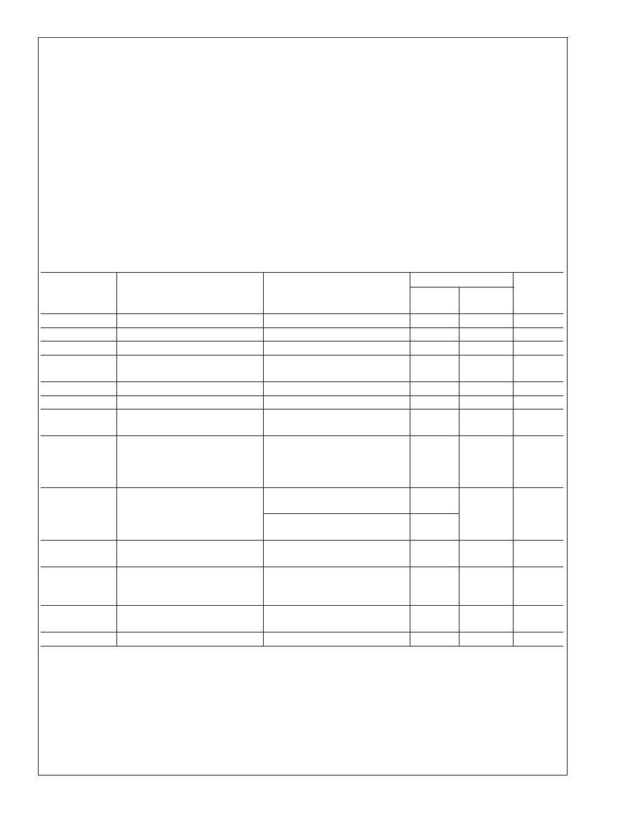
Electrical Characteristics V
DD
= 12V
(Notes 1, 2)
The following specifications apply for V
DD
= 12V, A
V
= 0dB (SE) or 6dB (BTL) unless otherwise specified. Limits apply for T
A
=
25∞C.
Symbol
Parameter
Conditions
LM4950
Units
(Limits)
Typical
(Note 6)
Limit
(Notes 7, 8)
I
DD
Quiescent Power Supply Current
V
IN
= 0V, I
O
= 0A, No Load
16
30
mA (max)
I
SD
Shutdown Current
V
SHUTDOWN
= GND (Note 9)
40
80
µA (max)
V
OS
Offset Voltage
V
IN
= 0V, RL = 8
5
30
mV (max)
V
SDIH
Shutdown Voltage Input High
2.0
V
DD
/2
V (min)
V (max)
V
SDIL
Shutdown Voltage Input Low
0.4
V (max)
T
WU
Wake-up Time
C
B
= 10µF
440
ms
TSD
Thermal Shutdown Temperature
170
150
190
∞C (min)
∞C (max)
P
O
Output Power
f = 1kHz
R
L
= 4
SE, Single Channel,
THD+N = 1%
R
L
= 8
BTL, THD+N = 10%
3.1
7.5
3.0
W (min)
THD+N
Total Harmomic Distortion + Noise
P
O
= 2.5Wrms; f = 1kHz;
R
L
= 4
SE
0.05
%
P
O
= 2.5Wrms; A
V
= 10; f = 1kHz;
R
L
= 4
, SE
0.14
e
OS
Output Noise
A-Weighted Filter, V
IN
= 0V,
Input Referred
10
µV
X
TALK
Channel Separation
f
IN
= 1kHz, P
O
= 1W, SE Mode
R
L
= 8
R
L
= 4
76
70
dB
PSRR
Power Supply Rejection Ratio
V
RIPPLE
= 200mV
p-p
, f = 1kHz,
R
L
= 8
, BTL
70
56
dB (min)
I
OL
Output Current Limit
V
IN
= 0V, R
L
= 500m
5
A
Note 1: All voltages are measured with respect to the GND pin, unless otherwise specified.
Note 2: Absolute Maximum Ratings indicate limits beyond which damage to the device may occur. Operating Ratings indicate conditions for which the device is
functional, but do not guarantee specific performance limits. Electrical Characteristics state DC and AC electrical specifications under particular test conditions which
guarantee specific performance limits. This assumes that the device is within the Operating Ratings. Specifications are not guaranteed for parameters where no limit
is given, however, the typical value is a good indication of device performance.
Note 3: The maximum power dissipation must be derated at elevated temperatures and is dictated by T
JMAX
,
JA
, and the ambient temperature, T
A
. The maximum
allowable power dissipation is P
DMAX
= (T
JMAX
- T
A
) /
JA
or the given in Absolute Maximum Ratings, whichever is lower. For the LM4950 typical application (shown
in Figure 1) with V
DD
= 12V, R
L
= 4
stereo operation the total power dissipation is 3.65W.
JA
= 20∞C/W for both TO263 and TO220 packages mounted to 16in
2
heatsink surface area.
Note 4: Human body model, 100pF discharged through a 1.5 k
resistor.
Note 5: Machine Model, 220pF≠240pF discharged through all pins.
LM4950
www.national.com
3
Electrical Characteristics V
DD
= 12V
(Notes 1, 2) (Continued)
Note 6: Typicals are measured at 25∞C and represent the parametric norm.
Note 7: Limits are guaranteed to National's AOQL (Average Outgoing Quality Level).
Note 8: Datasheet min/max specification limits are guaranteed by design, test, or statistical analysis.
Note 9: Shutdown current is measured in a normal room environment. The Shutdown pin should be driven as close as possible to GND for minimum shutdown
current.
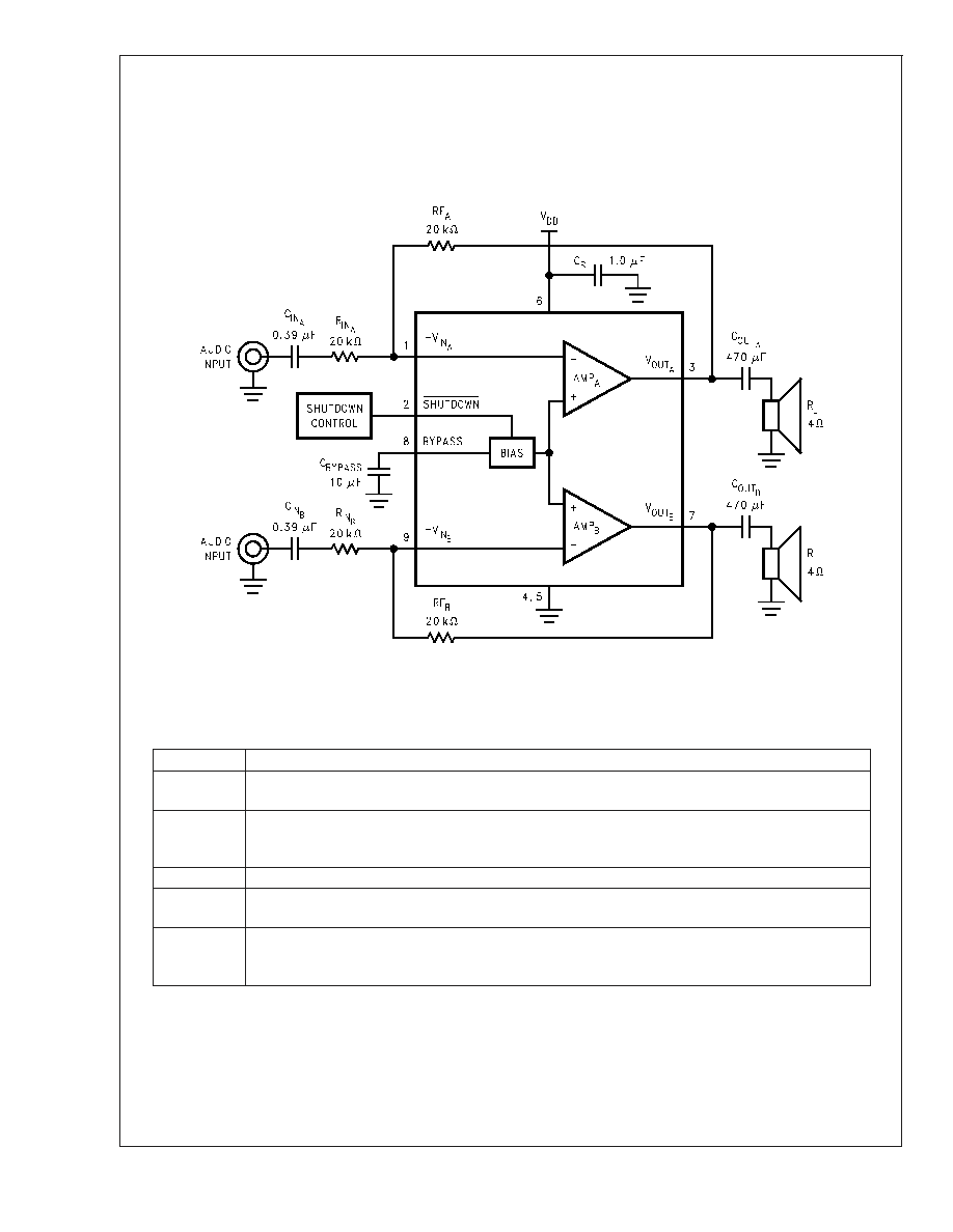
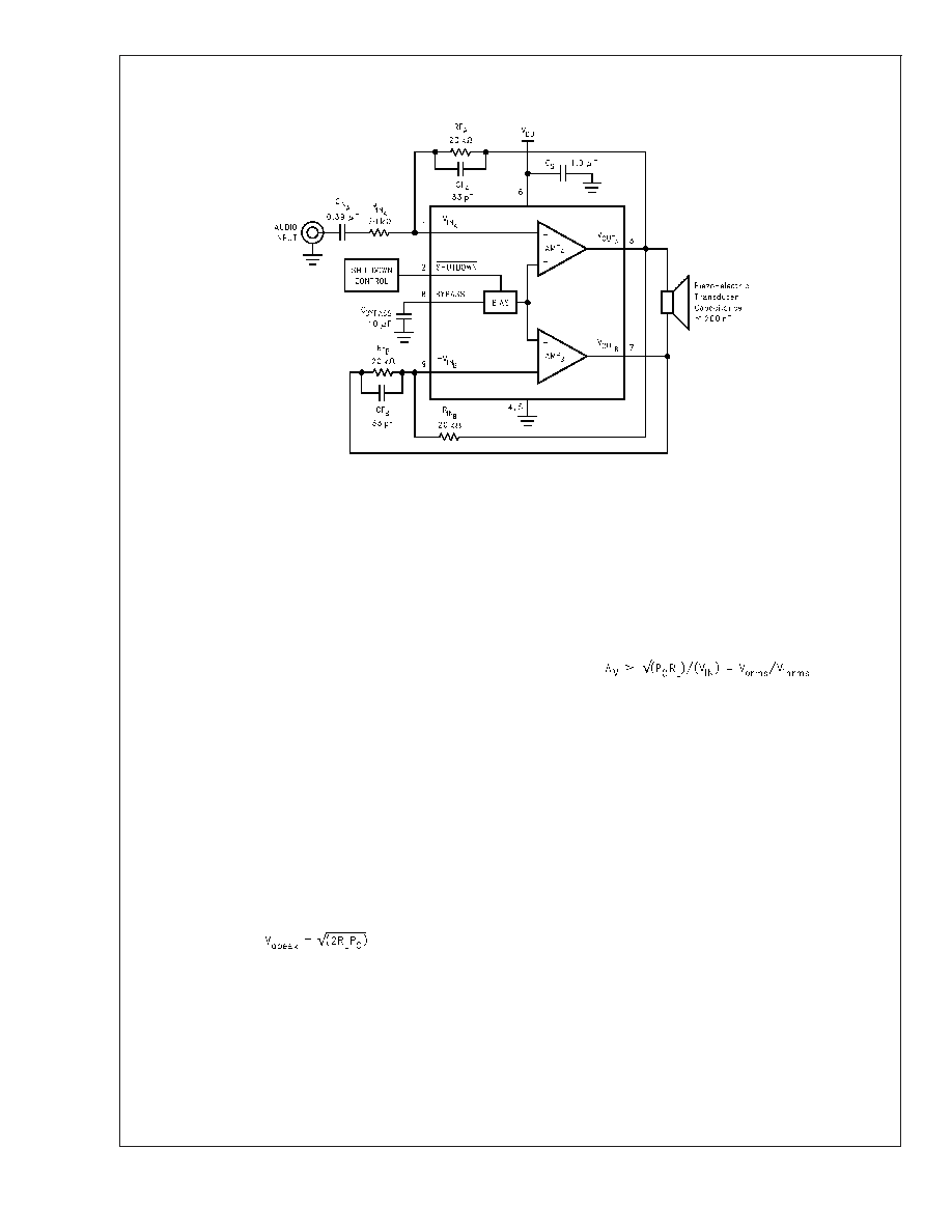
External Components Description
Refer to (Figure 1.)
Components
Functional Description
1. R
IN
This is the inverting input resistance that, along with R
F
, sets the closed-loop gain. Input resistance R
IN
and input capacitance C
IN
form a high pass filter. The filter's cutoff frequency is f
c
= 1/(2
R
IN
C
IN
).
2. C
IN
This is the input coupling capacitor. It blocks DC voltage at the amplifier's inverting input. C
IN
and R
IN
create a highpass filter. The filter's cutoff frequency is f
C
= 1/(2
R
IN
C
IN
). Refer to the SELECTING
EXTERNAL COMPONENTS, for an explanation of determining C
IN
's value.
3. R
F
This is the feedback resistance that, along with R
i
, sets closed-loop gain.
4. C
S
The supply bypass capacitor. Refer to the POWER SUPPLY BYPASSING section for information about
properly placing, and selecting the value of, this capacitor.
5. C
BYPASS
This capacitor filters the half-supply voltage present on the BYPASS pin. Refer to the Application section,
SELECTING EXTERNAL COMPONENTS, for information about properly placing, and selecting the
value of, this capacitor.
20047072
FIGURE 2. Typical Stereo Single-Ended (SE) Audio Amplifier Application Circuit
LM4950
www.national.com
4
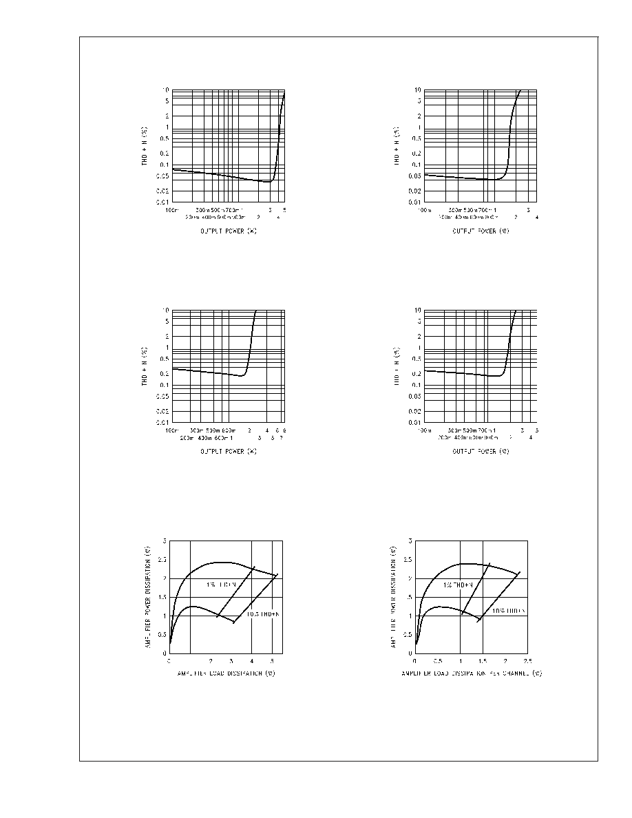
Typical Performance Characteristics
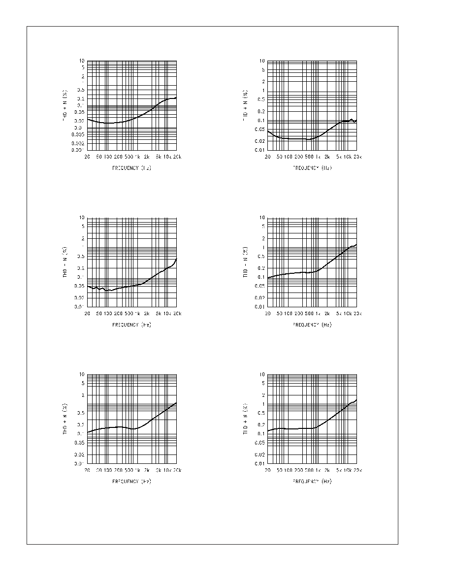
THD+N vs Frequency
THD+N vs Frequency
200470B2
V
DD
= 12V, R
L
= 8
,
BTL operation, P
OUT
= 1W
200470B3
V
DD
= 12V, R
L
= 8
,
BTL operation, P
OUT
= 3W
THD+N vs Frequency
THD+N vs Frequency
200470B4
V
DD
= 12V, R
L
= 8
,
BTL operation, P
OUT
= 5W
200470D5
V
DD
= 12V, R
L
= 8
,
BTL operation, BTLA
V
= 20, P
OUT
= 1W
THD+N vs Frequency
THD+N vs Frequency
200470D4
V
DD
= 12V, R
L
= 8
,
BTL operation, BTLA
V
= 20, P
OUT
= 3W
200470D6
V
DD
= 12V, R
L
= 8
,
BTL operation, BTLA
V
= 20, P
OUT
= 5W
LM4950
www.national.com
5
Typical Performance Characteristics
(Continued)
THD+N vs Frequency
THD+N vs Frequency
20047099
V
DD
= 12V, R
L
= 4
, SE operation,
both channels driven and loaded (average shown),
P
OUT
= 1W, A
V
= 1
200470A0
V
DD
= 12V, R
L
= 4
, SE operation,
both channels driven and loaded (average shown),
P
OUT
= 2.5W, A
V
= 1
THD+N vs Frequency
THD+N vs Output Power
200470A1
V
DD
= 12V, R
L
= 8
, SE operation,
both channels driven and loaded (average shown),
P
OUT
= 1W, A
V
= 1
200470A9
V
DD
= 12V, R
L
= 8
,
BTL operation, f
IN
= 1kHz
THD+N vs Output Power
THD+N vs Output Power
200470D0
V
DD
= 12V, R
L
= 8
,
BTL operation, BTLA
V
= 20, f
IN
= 1kHz
200470D1
V
DD
= 12V, R
L
= 16
,
BTL operation, BTLA
V
= 20, f
IN
= 1kHz
LM4950
www.national.com
6
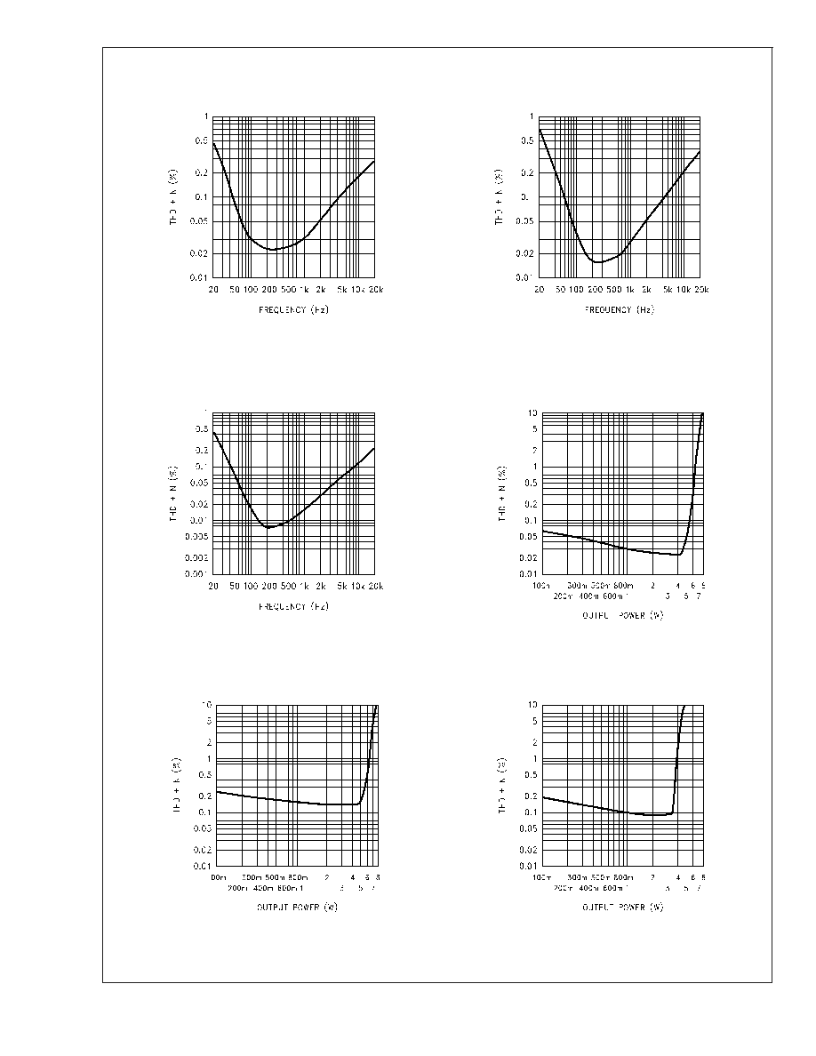
Typical Performance Characteristics
(Continued)
THD+N vs Output Power
THD+N vs Output Power
200470D9
V
DD
= 12V, R
L
= 4
, SE operation,
both channels driven and loaded (average shown),
f
IN
= 1kHz
200470E0
V
DD
= 12V, R
L
= 8
, SE operation,
both channels driven and loaded (average shown),
f
IN
= 1kHz
THD+N vs Output Power
THD+N vs Output Power
200470E1
V
DD
= 12V, R
L
= 16
, SE operation,
both channels driven and loaded (average shown),
f
IN
= 1kHz
200470C7
V
DD
= 12V, R
L
= 4
, SE operation, A
V
= 10
both channels driven and loaded (average shown),
f
IN
= 1kHz
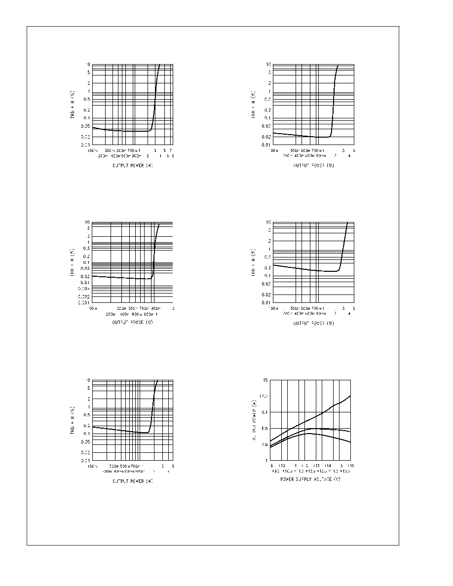
THD+N vs Output Power
Output Power vs Power Supply Voltage
200470C6
V
DD
= 12V, R
L
= 8
, SE operation, A
V
= 10
both channels driven and loaded (average shown),
f
IN
= 1kHz
200470C3
R
L
= 8
, BTL, f
IN
= 1kHz,
at (from top to bottom at 12V): THD+N = 10%
THD+N = 1%, THD+N = 0.2%
LM4950
www.national.com
7

Typical Performance Characteristics
(Continued)
Output Power vs Power Supply Voltage
Output Power vs Power Supply Voltage
200470C5
R
L
= 4
, SE operation,
both channels driven and loaded (average shown),
at (from top to bottom at 12V): THD+N = 10%,
THD+N = 1%
200470C4
R
L
= 8
, SE operation, f
IN
= 1kHz,
both channels driven and loaded (average shown),
at (from top to bottom at 12V): THD+N = 10%,
THD+N = 1%
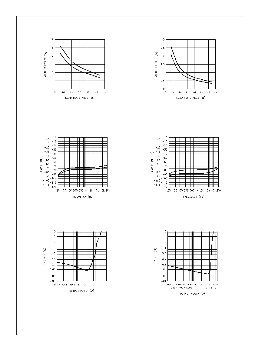
Power Supply Rejection vs Frequency
Power Supply Rejection vs Frequency
200470B9
V
DD
= 12V, R
L
= 8
, BTL operation,
V
RIPPLE
= 200mV
p-p
, at (from top to bottom at 60Hz):
C
BYPASS
= 1µF, C
BYPASS
= 4.7µF, C
BYPASS
= 10µF,
200470B8
V
DD
= 12V, R
L
= 8
, SE operation,
V
RIPPLE
= 200mV
p-p
, at (from top to bottom at 60Hz):
C
BYPASS
= 1µF, C
BYPASS
= 4.7µF, C
BYPASS
= 10µF,
Power Supply Rejection vs Frequency
Power Supply Rejection vs Frequency
200470D7
V
DD
= 12V, R
L
= 8
, BTL operation, V
RIPPLE
= 200mV
p-p
,
A
V
= 20, at (from top to bottom at 60Hz):
C
BYPASS
= 1µF, C
BYPASS
= 4.7µF, C
BYPASS
= 10µF
200470D8
V
DD
= 12V, R
L
= 8
, SE operation, V
RIPPLE
= 200mV
p-p
,
A
V
= 10, at (from top to bottom at 60Hz):
C
BYPASS
= 1µF, C
BYPASS
= 4.7µF, C
BYPASS
= 10µF
LM4950
www.national.com
8
Typical Performance Characteristics
(Continued)
Total Power Dissipation vs Load Dissipation
Total Power Dissipation vs Load Dissipation
20047084
V
DD
= 12V, BTL operation, f
IN
= 1kHz,
at (from top to bottom at 3W):
R
L
= 8
, R
L
= 16
20047081
V
DD
= 12V, SE operation, f
IN
= 1kHz,
at (from top to bottom at 1W):
R
L
= 4
, R
L
= 8
Output Power vs Load Resistance
Output Power vs Load Resistance
20047094
V
DD
= 12V, BTL operation, f
IN
= 1kHz,
at (from top to bottom at 15
):
THD+N = 10%, THD+N = 1%
20047091
V
DD
= 12V, SE operation, f
IN
= 1kHz,
both channels driven and loaded, at (from top to bottom
at 15
):
THD+N = 10%, THD+N = 1%
Channel-to-Channel Crosstalk vs Frequency
Channel-to-Channel Crosstalk vs Frequency
20047098
V
DD
= 12V, R
L
= 4
, P
OUT
= 1W, SE operation,
at (from top to bottom at 1kHz): V
INB
driven,
V
OUTA
measured; V
INA
driven, V
OUTB
measured
200470A3
V
DD
= 12V, R
L
= 8
, P
OUT
= 1W, SE operation,
at (from top to bottom at 1kHz): V
INB
driven,
V
OUTA
measured; V
INA
driven, V
OUTB
measured
LM4950
www.national.com
9
Typical Performance Characteristics
(Continued)
THD+N vs Output Power
THD+N vs Output Power
200470B5
V
DD
= 9.6V, R
L
= 8
,
BTL operation, f
IN
= 1kHz
200470E2
V
DD
= 9.6V, R
L
= 4
,
SE operation, f
IN
= 1kHz
both channels driven and loaded (average shown)
THD+N vs Output Power
THD+N vs Output Power
200470D2
V
DD
= 9.6V, R
L
= 8
, BTL operation,
BTLA
V
= 20, f
IN
= 1kHz
200470C8
V
DD
= 9.6V, R
L
= 4
, SE operation,
AV = 10, f
IN
= 1kHz
both channels driven and loaded (average shown)
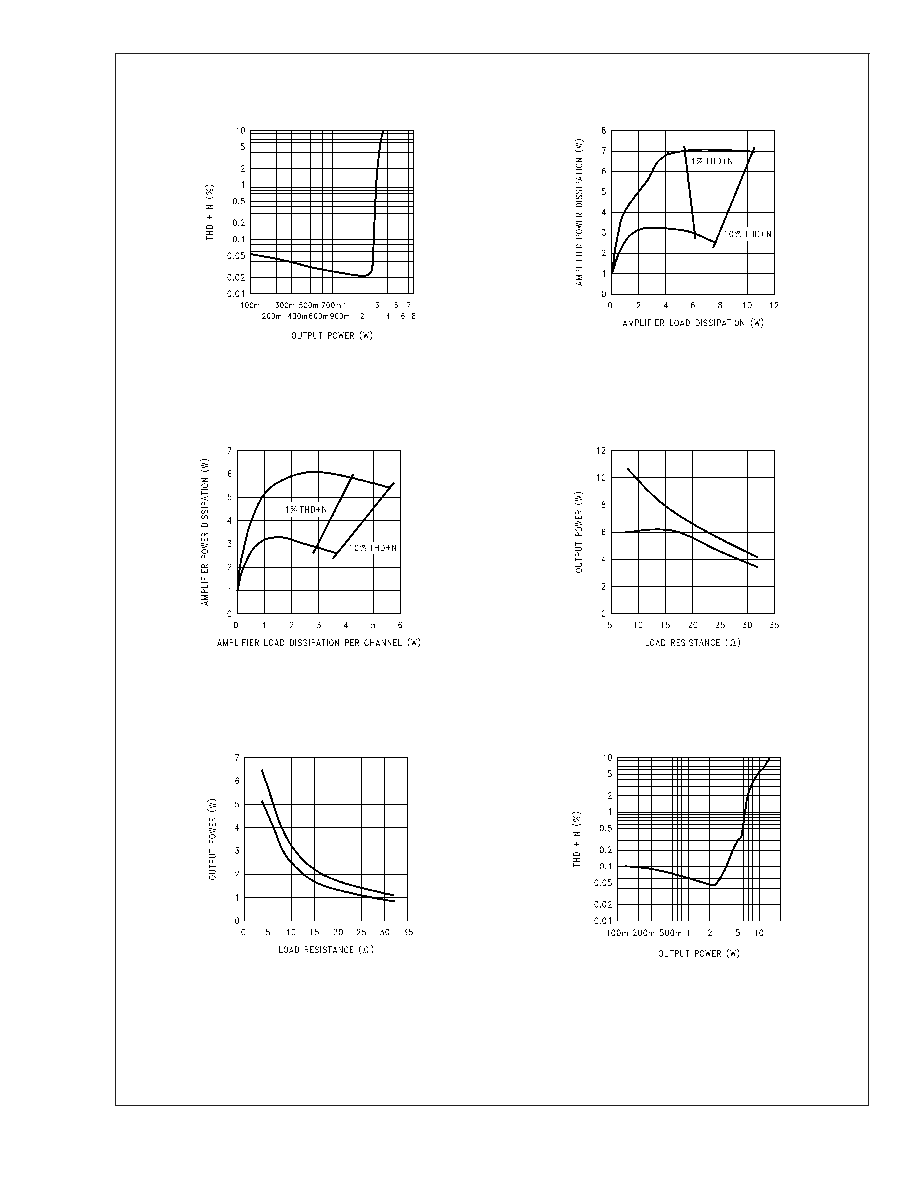
Total Power Dissipation vs Load Dissipation
Total Power Dissipation vs Load Dissipation per
Channel
20047085
V
DD
= 9.6V, BTL operation, f
IN
= 1kHz
at (from top to bottom at 2W):
R
L
= 8
, R
L
= 16
20047082
V
DD
= 9.6V, SE operation, f
IN
= 1kHz,
at (from top to bottom at 1W):
R
L
= 4
, R
L
= 8
LM4950
www.national.com
10
Typical Performance Characteristics
(Continued)
Output Power vs Load Resistance
Output Power vs Load Resistance
20047095
V
DD
= 9.6V, BTL operation, f
IN
= 1kHz,
at (from top to bottom at 15
):
THD+N = 10%, THD+N = 1%
20047092
V
DD
= 9.6V, SE operation, f
IN
= 1kHz,
both channels driven and loaded, at (from top to bottom
at 15
):
THD+N = 10%, THD+N = 1%
Channel-to Channel Crosstalk vs Frequency
Channel-to Channel Crosstalk vs Frequency
20047096
V
DD
= 9.6V, R
L
= 4
, P
OUT
= 1W, SE operation,
at (from top to bottom at 1kHz): V
INB
driven, V
OUTA
measured; V
INA
driven, V
OUTB
measured
200470A4
V
DD
= 9.6V, R
L
= 8
, P
OUT
= 1W, SE operation,
at (from top to bottom at 1kHz): V
INB
driven, V
OUTA
measured; V
INA
driven, V
OUTB
measured
THD+N vs Output Power
THD+N vs Output Power
200470C0
V
DD
= 15V, R
L
= 8
,
BTL operation, f
IN
= 1kHz
200470C2
V
DD
= 15V, R
L
= 4
,
SE operation, f
IN
= 1kHz
both channels driven and loaded (average shown)
LM4950
www.national.com
11
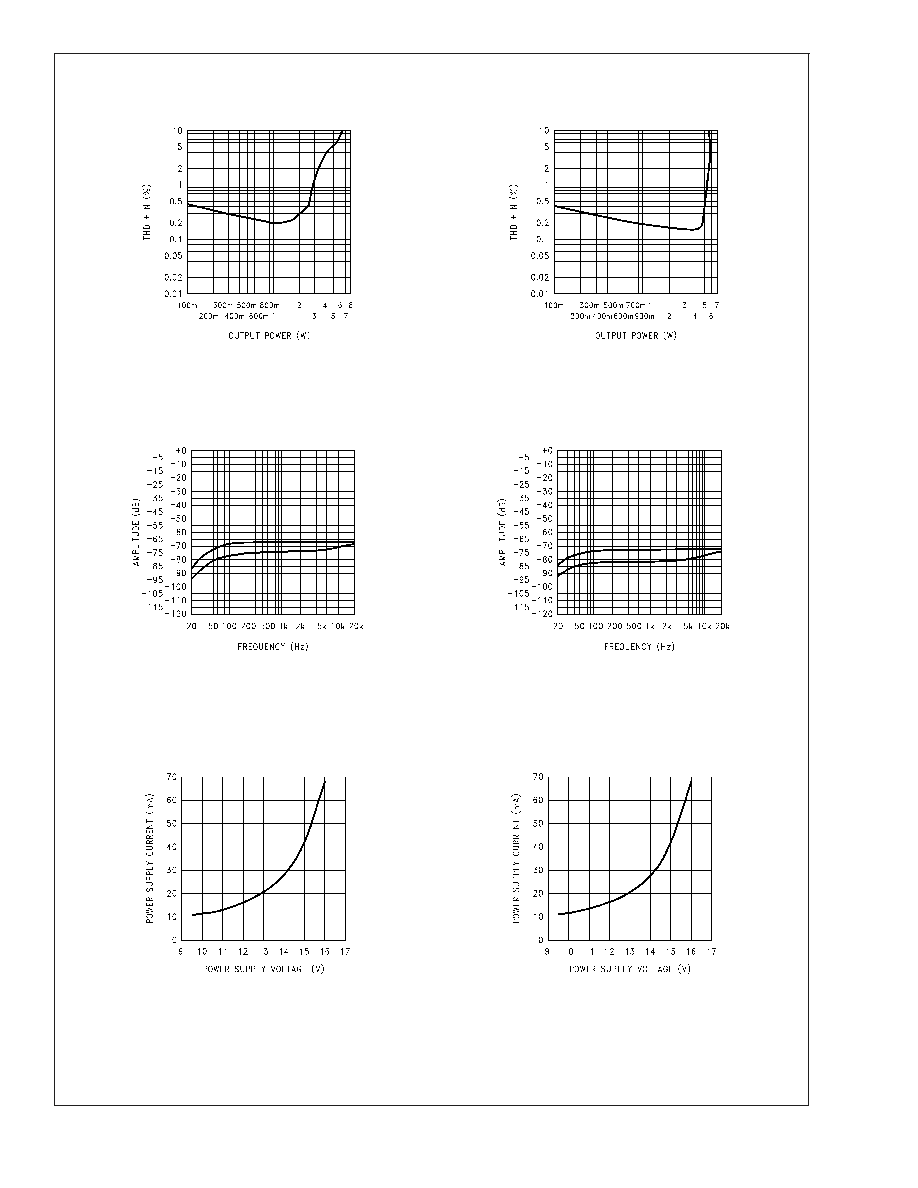
Typical Performance Characteristics
(Continued)
THD+N vs Output Power
Total Power Dissipation vs Load Dissipation
200470E3
V
DD
= 15V, R
L
= 8
,
SE operation, f
IN
= 1kHz
both channels driven and loaded (average shown)
20047083
V
DD
= 15V, BTL operation, f
IN
= 1kHz,
at (from top to bottom at 4W): R
L
= 8
, R
L
= 16
Total Power Dissipation vs Load Dissipation per
Channel
Output Power vs Load Resistance
20047080
V
DD
= 15V, SE operation, f
IN
= 1kHz,
at (from top to bottom at 2W): R
L
= 4
, R
L
= 8
20047093
V
DD
= 15V, BTL operation, f
IN
= 1kHz,
at (from top to bottom at 15
):
THD+N = 10%, THD+N = 1%
Output Power vs Load Resistance
THD+N vs Output Power
20047090
V
DD
= 15V, SE operation, f
IN
= 1kHz,
both channels driven and loaded,
at (from top to bottom at 15
): THD+N = 10%, THD+N =
1%
200470B6
V
DD
= 16V, R
L
= 8
,
BTL operation, f
IN
= 1kHz
LM4950
www.national.com
12
Typical Performance Characteristics
(Continued)
THD+N vs Output Power
THD+N vs Output Power
200470D3
V
DD
= 16V, R
L
= 8
,
BTL operation, f
IN
= 1kHz, BTLA
V
= 20
200470C9
V
DD
= 16V, R
L
= 4
, A
V
= 10
SE operation, f
IN
= 1kHz,
both channels driven and loaded (average shown)
Channel-to-Channel Crosstalk vs Frequency
Channel-to-Channel Crosstalk vs Frequency
20047097
V
DD
= 16V, R
L
= 4
, P
OUT
= 1W, SE operation
at (from top to bottom at 1kHz): V
INB
driven, V
OUTA
measured;
V
INA
driven, V
OUTB
measured
200470A2
V
DD
= 16V, R
L
= 8
, P
OUT
= 1W, SE operation
at (from top to bottom at 1kHz): V
INB
driven, V
OUTA
measured;
V
INA
driven, V
OUTB
measured
Power Supply Current vs Power Supply Voltage
Power Supply Current vs Power Supply Voltage
200470A6
R
L
= 8
, BTL operation
V
IN
= 0V, R
SOURCE
= 50
200470A7
R
L
= 4
, SE operation
V
IN
= 0V, R
SOURCE
= 50
LM4950
www.national.com
13
Typical Performance Characteristics
(Continued)
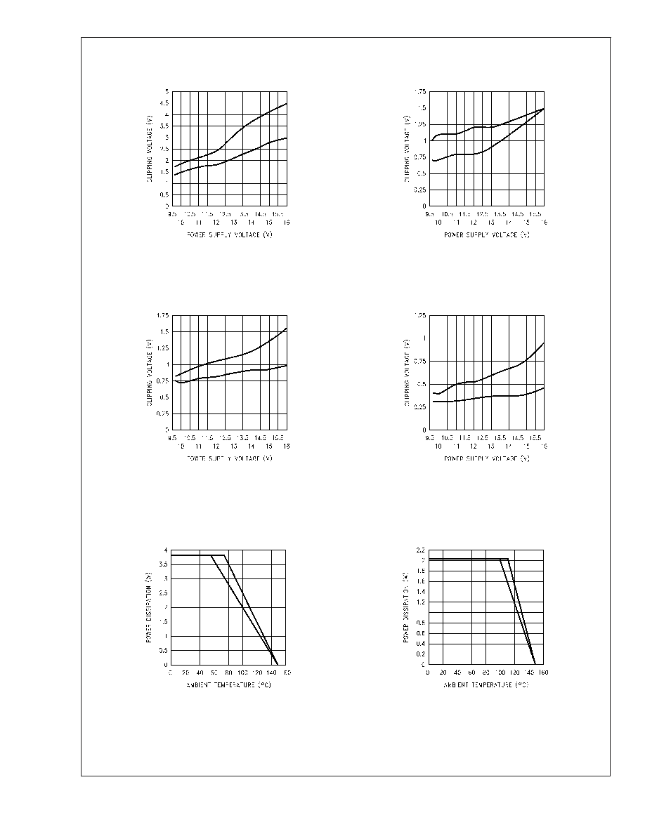
Clipping Voltage vs Power Supply Voltage
Clipping Voltage vs Power Supply Voltage
20047088
R
L
= 8
, BTL operation, f
IN
= 1kHz
at (from top to bottom at 12V):
positive signal swing, negative signal swing
20047086
R
L
= 16
, BTL operation, f
IN
= 1kHz
at (from to bottom at 12V):
positive signal swing, negative signal swing
Clipping Voltage vs Power Supply Voltage
Clipping Voltage vs Power Supply Voltage
20047089
R
L
= 4
, SE operation, f
IN
= 1kHz
both channels driven and loaded, at (from top to bottom
at 13V):
negative signal swing, positive signal swing
20047087
R
L
= 8
, SE operation, f
IN
= 1kHz
both channels driven and loaded, at (from to bottom at
13V):
negative signal swing, positive signal swing
Power Dissipation vs Ambient Temperature
Power Dissipation vs Ambient Temperature
200470E6
V
DD
= 12V, R
L
= 8
(BTL), f
IN
= 1kHz,
(from to bottom at 80∞C): 16in
2
copper plane heatsink
area,
8in
2
copper plane heatsink area
200470E4
V
DD
= 12V, R
L
= 8
(SE), f
IN
= 1kHz,
(from to bottom at 120∞C): 16in
2
copper plane heatsink
area,
8in
2
copper plane heatsink area
LM4950
www.national.com
14
Application Information
HIGH VOLTAGE BOOMER WITH INCREASED OUTPUT
POWER
Unlike previous 5V Boomer
Æ
amplifiers, the LM4950 is de-
signed to operate over a power supply voltages range of
9.6V to 16V. Operating on a 12V power supply, the LM4950
will deliver 7.5W into an 8
BTL load with no more than 10%
THD+N.
BRIDGE CONFIGURATION EXPLANATION
As shown in Figure 3, the LM4950 consists of two opera-
tional amplifiers that drive a speaker connected between
their outputs. The value of external input and feedback re-
sistors determine the gain of each amplifier. Resistors RIN
A
and RF
A
set the closed-loop gain of AMP
A
, whereas two
20k
resistors set AMP
B
's gain to -1. The LM4950 drives a
load, such as a speaker, connected between the two ampli-
fier outputs, VOUT
A
and VOUT
B
. Figure 3 shows that
AMP
A
's output serves as AMP
B
's input. This results in both
amplifiers producing signals identical in magnitude, but 180∞
out of phase. Taking advantage of this phase difference, a
load is placed between AMP
A
and AMP
B
and driven differ-
entially (commonly referred to as "bridge mode"). This re-
sults in a differential, or BTL, gain of
A
VD
= 2(R
f
/ R
i
)
(1)
Bridge mode amplifiers are different from single-ended am-
plifiers that drive loads connected between a single amplifi-
er's output and ground. For a given supply voltage, bridge
mode has a distinct advantage over the single-ended con-
figuration: its differential output doubles the voltage swing
across the load. Theoretically, this produces four times the
output power when compared to a single-ended amplifier
under the same conditions. This increase in attainable output
power assumes that the amplifier is not current limited and
that the output signal is not clipped. To ensure minimum
output signal clipping when choosing an amplifier's closed-
loop gain, refer to the AUDIO POWER AMPLIFIER DESIGN
section.
Another advantage of the differential bridge output is no net
DC voltage across the load. This is accomplished by biasing
AMP1's and AMP2's outputs at half-supply. This eliminates
the coupling capacitor that single supply, single-ended am-
plifiers require. Eliminating an output coupling capacitor in a
typical single-ended configuration forces a single-supply am-
plifier's half-supply bias voltage across the load. This in-
creases internal IC power dissipation and may permanently
damage loads such as speakers.
POWER DISSIPATION
Power dissipation is a major concern when designing a
successful single-ended or bridged amplifier. Equation (2)
states the maximum power dissipation point for a single-
ended amplifier operating at a given supply voltage and
driving a specified output load.
20047078
FIGURE 3. Typical LM4950 BTL Application Circuit
LM4950
www.national.com
15

Application Information
(Continued)
P
DMAX-SE
= (V
DD
)
2
/ (2
2
R
L
):
Single Ended
(2)
The LM4950's dissipation is twice the value given by Equa-
tion (2) when driving two SE loads. For a 12V supply and two
8
SE loads, the LM4950's dissipation is 1.82W.
The LM4950's dissipation when driving a BTL load is given
by Equation (3). For a 12V supply and a single 8
BTL load,
the dissipation is 3.65W.
P
DMAX-MONOBTL
= 4(V
DD
)
2
/ 2
2
R
L
:
Bridge Mode (3)
The maximum power dissipation point given by Equation (3)
must not exceed the power dissipation given by Equation
(4):
P
DMAX
' = (T
JMAX
- T
A
) /
JA
(4)
The LM4950's T
JMAX
= 150∞C. In the TS package, the
LM4950's
JA
is 20∞C/W when the metal tab is soldered to a
copper plane of at least 16in
2
. This plane can be split be-
tween the top and bottom layers of a two-sided PCB. Con-
nect the two layers together under the tab with a 5x5 array of
vias. For the TA package, use an external heatsink with a
thermal impedance that is less than 20∞C/W. At any given
ambient temperature T
A
, use Equation (4) to find the maxi-
mum internal power dissipation supported by the IC packag-
ing. Rearranging Equation (4) and substituting P
DMAX
for
P
DMAX
' results in Equation (5). This equation gives the maxi-
mum ambient temperature that still allows maximum stereo
power dissipation without violating the LM4950's maximum
junction temperature.
T
A
= T
JMAX
- P
DMAX-MONOBTL
JA
(5)
For a typical application with a 12V power supply and a BTL
8
load, the maximum ambient temperature that allows
maximum stereo power dissipation without exceeding the
maximum junction temperature is approximately 77∞C for the
TS package.
T
JMAX
= P
DMAX-MONOBTL
JA
+ T
A
(6)
Equation (6) gives the maximum junction temperature
T
JMAX
. If the result violates the LM4950's 150∞C, reduce the
maximum junction temperature by reducing the power sup-
ply voltage or increasing the load resistance. Further allow-
ance should be made for increased ambient temperatures.
The above examples assume that a device is operating
around the maximum power dissipation point. Since internal
power dissipation is a function of output power, higher am-
bient temperatures are allowed as output power or duty
cycle decreases.
If the result of Equation (3) is greater than that of Equation
(4), then decrease the supply voltage, increase the load
impedance, or reduce the ambient temperature. Further,
ensure that speakers rated at a nominal 4
(SE operation)
or 8
(BTL operation) do not fall below 3 or 6, respec-
tively. If these measures are insufficient, a heat sink can be
added to reduce
JA
. The heat sink can be created using
additional copper area around the package, with connec-
tions to the ground pins, supply pin and amplifier output pins.
Refer to the Typical Performance Characteristics curves
for power dissipation information at lower output power lev-
els.
POWER SUPPLY VOLTAGE LIMITS
Continuous proper operation is ensured by never exceeding
the voltage applied to any pin, with respect to ground, as
listed in the Absolute Maximum Ratings section.
POWER SUPPLY BYPASSING
As with any power amplifier, proper supply bypassing is
critical for low noise performance and high power supply
rejection. Applications that employ a voltage regulator typi-
cally use a 10µF in parallel with a 0.1µF filter capacitors to
stabilize the regulator's output, reduce noise on the supply
line, and improve the supply's transient response. However,
their presence does not eliminate the need for a local 1.0µF
tantalum bypass capacitance connected between the
LM4950's supply pins and ground. Do not substitute a ce-
ramic capacitor for the tantalum. Doing so may cause oscil-
lation. Keep the length of leads and traces that connect
capacitors between the LM4950's power supply pin and
ground as short as possible. Connecting a 10µF capacitor,
C
BYPASS
, between the BYPASS pin and ground improves
the internal bias voltage's stability and improves the amplifi-
er's PSRR. The PSRR improvements increase as the by-
pass pin capacitor value increases. Too large, however,
increases turn-on time and can compromise the amplifier's
click and pop performance. The selection of bypass capaci-
tor values, especially C
BYPASS
, depends on desired PSRR
requirements, click and pop performance (as explained in
the section, SELECTING EXTERNAL COMPONENTS),
system cost, and size constraints.
MICRO-POWER SHUTDOWN
The LM4950 features an active-low micro-power shutdown
mode. When active, the LM4950's micro-power shutdown
feature turns off the amplifier's bias circuitry, reducing the
supply current. The low 40µA typical shutdown current is
achieved by applying a voltage to the SHUTDOWN pin that
is as near to GND as possible. A voltage that is greater than
GND may increase the shutdown current.
There are a few methods to control the micro-power shut-
down. These include using a single-pole, single-throw switch
(SPST), a microprocessor, or a microcontroller. When using
a switch, connect a 100k
pull-up resistor between the
SHUTDOWN pin and V
DD
and a second 100k
resistor in
parallel with the SPST switch connected between the SHUT-
DOWN pin and GND. The two resistors form a voltage
divider that ensures that the voltage applied to the SHUT-
DOWN pin does not exceed V
DD
/2. Select normal amplifier
operation by opening the switch. Closing the switch applies
GND to the SHUTDOWN pin, activating micro-power shut-
down. The switch and resistor guarantee that the SHUT-
DOWN pin will not float. This prevents unwanted state
changes. In a system with a microprocessor or a microcon-
troller, use a digital output to apply the active-state voltage to
the SHUTDOWN pin. Again, ensure that the microcontroller
or microprocessor logic-high signal does not exceed the
LM4950's V
DD
/2 SHUTDOWN signal limit.
LM4950
www.national.com
16
Application Information
(Continued)
SELECTING EXTERNAL COMPONENTS
Input Capacitor Value Selection
Two quantities determine the value of the input coupling
capacitor: the lowest audio frequency that requires amplifi-
cation and desired output transient suppression.
As shown in Figure 3, the input resistor (R
IN
) and the input
capacitor (C
IN
) produce a high pass filter cutoff frequency
that is found using Equation (7).
f
c
= 1/2
R
i
C
i
(7)
As an example when using a speaker with a low frequency
limit of 50Hz, C
i
, using Equation (7) is 0.159µF. The 0.39µF
C
INA
shown in Figure 3 allows the LM4950 to drive high
efficiency, full range speaker whose response extends below
30Hz.
Bypass Capacitor Value
Besides minimizing the input capacitor size, careful consid-
eration should be paid to value of C
BYPASS
, the capacitor
connected to the BYPASS pin. Since C
BYPASS
determines
how fast the LM4950 settles to quiescent operation, its value
is critical when minimizing turn-on pops. The slower the
LM4950's outputs ramp to their quiescent DC voltage (nomi-
nally V
DD
/2), the smaller the turn-on pop. Choosing C
BYPASS
equal to 10µF along with a small value of C
IN
(in the range of
0.1µF to 0.39µF), produces a click-less and pop-less shut-
down function. As discussed above, choosing C
IN
no larger
than necessary for the desired bandwidth helps minimize
clicks and pops.
OPTIMIZING CLICK AND POP REDUCTION
PERFORMANCE
The LM4950 contains circuitry that eliminates turn-on and
shutdown transients ("clicks and pops"). For this discussion,
turn-on refers to either applying the power supply voltage or
when the micro-power shutdown mode is deactivated.
As the V
DD
/2 voltage present at the BYPASS pin ramps to its
final value, the LM4950's internal amplifiers are configured
as unity gain buffers and are disconnected from the AMP
A
and AMP
B
pins. An internal current source charges the ca-
pacitor connected between the BYPASS pin and GND in a
controlled manner. Ideally, the input and outputs track the
voltage applied to the BYPASS pin. The gain of the internal
amplifiers remains unity until the voltage applied to the BY-
PASS pin.
The gain of the internal amplifiers remains unity until the
voltage on the bypass pin reaches V
DD
/2. As soon as the
voltage on the bypass pin is stable, the device becomes fully
operational and the amplifier outputs are reconnected to
their respective output pins. Although the BYPASS pin cur-
rent cannot be modified, changing the size of C
BYPASS
alters
the device's turn-on time. Here are some typical turn-on
times for various values of C
BYPASS
:
C
B
(µF)
T
ON
(ms)
1.0
120
2.2
120
4.7
200
10
440
In order eliminate "clicks and pops", all capacitors must be
discharged before turn-on. Rapidly switching V
DD
may not
allow the capacitors to fully discharge, which may cause
"clicks and pops".
There is a relationship between the value of C
IN
and
C
BYPASS
that ensures minimum output transient when power
is applied or the shutdown mode is deactivated. Best perfor-
mance is achieved by setting the time constant created by
C
IN
and R
i
+ R
f
to a value less than the turn-on time for a
given value of C
BYPASS
as shown in the table above.
DRIVING PIEZO-ELECTRIC SPEAKER TRANSDUCERS
The LM4950 is able to drive capacitive piezo-electric trans-
ducer loads that are less than equal to 200nF. Stable opera-
tion is assured by placing 33pF capacitors in parallel with the
20k
feedback resistors. The additional capacitors are
shown in Figure 4.
When driving piezo-electric tranducers, sound quality and
accoustic power is entirely dependent upon a transducer's
frequency response and efficiency. In this application, power
dissipated by the LM4950 is very low, typically less than
250mW when driving a 200nF piezo-electric transduce
(V
DD
= 12V).
LM4950
www.national.com
17
Application Information
(Continued)
AUDIO POWER AMPLIFIER DESIGN
Audio Amplifier Design: Driving 4W into an 8
BTL
The following are the desired operational parameters:
Power Output
4W
RMS
Load Impedance
8
Input Level
0.3V
RMS
(max)
Input Impedance
20k
Bandwidth
50Hz≠20kHz
±
0.25dB
The design begins by specifying the minimum supply voltage
necessary to obtain the specified output power. One way to
find the minimum supply voltage is to use the Output Power
vs Power Supply Voltage curve in the Typical Performance
Characteristics section. Another way, using Equation (8), is
to calculate the peak output voltage necessary to achieve
the desired output power for a given load impedance. To
account for the amplifier's dropout voltage, two additional
voltages, based on the Clipping Dropout Voltage vs Power
Supply Voltage in the Typical Performance Characteris-
tics curves, must be added to the result obtained by Equa-
tion (8). The result is Equation (9).
(8)
V
DD
= V
OUTPEAK
+ V
ODTOP
+ V
ODBOT
(9)
The Output Power vs. Power Supply Voltage graph for an 8
load indicates a minimum supply voltage of 10.2V. The com-
monly used 12V supply voltage easily meets this. The addi-
tional voltage creates the benefit of headroom, allowing the
LM4950 to produce peak output power in excess of 4W
without clipping or other audible distortion. The choice of
supply voltage must also not create a situation that violates
of maximum power dissipation as explained above in the
Power Dissipation section. After satisfying the LM4950's
power dissipation requirements, the minimum differential
gain needed to achieve 4W dissipation in an 8
BTL load is
found using Equation (10).
(10)
Thus, a minimum gain of 18.9 allows the LM4950's to reach
full output swing and maintain low noise and THD+N perfor-
mance. For this example, let A
V-BTL
= 19. The amplifier's
overall BTL gain is set using the input (RIN
A
) and feedback
(R) resistors of the first amplifier in the series BTL configu-
ration. Additionaly, A
V-BTL
is twice the gain set by the first
amplifier's R
IN
and R
f
. With the desired input impedance set
at 20k
, the feedback resistor is found using Equation (11).
R
f
/ R
IN
= A
V-BTL
/ 2
(11)
The value of R
f
is 190k
(choose 191k, the closest value).
The nominal output power is 4W.
The last step in this design example is setting the amplifier's
-3dB frequency bandwidth. To achieve the desired
±
0.25dB
pass band magnitude variation limit, the low frequency re-
sponse must extend to at least one-fifth the lower bandwidth
limit and the high frequency response must extend to at least
five times the upper bandwidth limit. The gain variation for
both response limits is 0.17dB, well within the
±
0.25dB-
desired limit. The results are an
f
L
= 50Hz / 5 = 10Hz
(12)
20047079
FIGURE 4. Piezo-electric Transducer Capacitance
200nF
LM4950
www.national.com
18

Application Information
(Continued)
and an
f
L
= 20kHz x 5 = 100kHz
(13)
As mentioned in the SELECTING EXTERNAL COMPO-
NENTS section, R
INA
and C
INA
create a highpass filter that
sets the amplifier's lower bandpass frequency limit. Find the
coupling capacitor's value using Equation (14).
C
i
= 1 / 2
R
IN
f
L
(14)
The result is
1 / (2
x20kx10Hz) = 0.795µF
Use a 0.82µF capacitor, the closest standard value.
The product of the desired high frequency cutoff (100kHz in
this example) and the differential gain A
VD
, determines the
upper passband response limit. With A
VD
= 7 and f
H
=
100kHz, the closed-loop gain bandwidth product (GBWP) is
700kHz. This is less than the LM4950's 3.5MHz GBWP. With
this margin, the amplifier can be used in designs that require
more differential gain while avoiding performance restricting
bandwidth limitations.
RECOMMENDED PRINTED CIRCUIT BOARD LAYOUT
Figure 5 through Figure 7 show the recommended two-layer
PC board layout that is optimized for the TO263-packaged,
SE-configured LM4950 and associated external compo-
nents. Figure 8 through Figure 10 show the recommended
two-layer PC board layout that is optimized for the TO263-
packaged, BTL-configured LM4950 and associated external
components. These circuits are designed for use with an
external 12V supply and 4
(min)(SE) or 8(min)(BTL)
speakers.
These circuit boards are easy to use. Apply 12V and ground
to the board's V
DD
and GND pads, respectively. Connect a
speaker between the board's OUT
A
and OUT
B
outputs.
Demonstration Board Layout
20047063
FIGURE 5. Recommended TS SE PCB Layout:
Top Silkscreen
LM4950
www.national.com
19
Demonstration Board Layout
(Continued)
20047064
FIGURE 6. Recommended TS SE PCB Layout:
Top Layer
20047065
FIGURE 7. Recommended TS SE PCB Layout:
Bottom Layer
LM4950
www.national.com
20
Demonstration Board Layout
(Continued)
20047066
FIGURE 8. Recommended TS BTL PCB Layout:
Top Silkscreen
20047067
FIGURE 9. Recommended TS BTL PCB Layout:
Top Layer
LM4950
www.national.com
21
Demonstration Board Layout
(Continued)
20047068
FIGURE 10. Recommended TS BTL PCB Layout:
Bottom Layer
LM4950
www.national.com
22
Physical Dimensions
inches (millimeters) unless otherwise noted
Order Number LM4950TS
NS Package Number TS9A
LM4950
www.national.com
23
Physical Dimensions
inches (millimeters) unless otherwise noted (Continued)
For Staggered Lead Non-Isolated Package
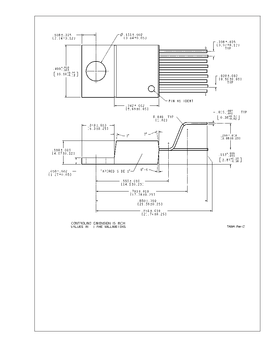
Order Number LM4950TA
NS Package Number TA09A
LM4950
www.national.com
24

Notes
LIFE SUPPORT POLICY
NATIONAL'S PRODUCTS ARE NOT AUTHORIZED FOR USE AS CRITICAL COMPONENTS IN LIFE SUPPORT
DEVICES OR SYSTEMS WITHOUT THE EXPRESS WRITTEN APPROVAL OF THE PRESIDENT AND GENERAL
COUNSEL OF NATIONAL SEMICONDUCTOR CORPORATION. As used herein:
1. Life support devices or systems are devices or
systems which, (a) are intended for surgical implant
into the body, or (b) support or sustain life, and
whose failure to perform when properly used in
accordance with instructions for use provided in the
labeling, can be reasonably expected to result in a
significant injury to the user.
2. A critical component is any component of a life
support device or system whose failure to perform
can be reasonably expected to cause the failure of
the life support device or system, or to affect its
safety or effectiveness.
BANNED SUBSTANCE COMPLIANCE
National Semiconductor certifies that the products and packing materials meet the provisions of the Customer Products
Stewardship Specification (CSP-9-111C2) and the Banned Substances and Materials of Interest Specification
(CSP-9-111S2) and contain no ``Banned Substances'' as defined in CSP-9-111S2.
National Semiconductor
Americas Customer
Support Center
Email: new.feedback@nsc.com
Tel: 1-800-272-9959
National Semiconductor
Europe Customer Support Center
Fax: +49 (0) 180-530 85 86
Email: europe.support@nsc.com
Deutsch Tel: +49 (0) 69 9508 6208
English
Tel: +44 (0) 870 24 0 2171
FranÁais Tel: +33 (0) 1 41 91 8790
National Semiconductor
Asia Pacific Customer
Support Center
Email: ap.support@nsc.com
National Semiconductor
Japan Customer Support Center
Fax: 81-3-5639-7507
Email: jpn.feedback@nsc.com
Tel: 81-3-5639-7560
www.national.com
LM4950
7.5W
Mono-BTL
or
3.1W
Stereo
Audio
Power
Amplifier
National does not assume any responsibility for use of any circuitry described, no circuit patent licenses are implied and National reserves the right at any time without notice to change said circuitry and specifications.