LM4950
7.5W Mono-BTL or 3.1W Stereo Audio Power Amplifier
General Description
The LM4950 is a dual audio power amplifier primarily de-
signed for demanding applications in flat panel monitors and
TV's. It is capable of delivering 3.1 watts per channel to a 4
single-ended load with less than 1% THD+N or 7.5 watts
mono BTL to an 8
load, with less than 10% THD+N from a
12V
DC
power supply.
Boomer audio power amplifiers were designed specifically to
provide high quality output power with a minimal amount of
external components. The LM4950 does not require boot-
strap capacitors or snubber circuits. Therefore, it is ideally
suited for display applications requiring high power and mini-
mal size.
The LM4950 features a low-power consumption active-low
shutdown mode. Additionally, the LM4950 features an inter-
nal thermal shutdown protection mechanism along with short
circuit protection.
The LM4950 contains advanced pop & click circuitry that
eliminates noises which would otherwise occur during
turn-on and turn-off transitions.
The LM4950 is a unity-gain stable and can be configured by
external gain-setting resistors.
Key Specifications
j
Quiscent Power Supply Current
16mA (typ)
j
P
OUT
(SE)
V
DD
= 12V, R
L
= 4
, 1% THD+N
3.1W (typ)
j
P
OUT
(BTL)
V
DD
= 12V, R
L
= 8
, 10% THD+N
7.5W (typ)
j
Shutdown current
40�A (typ)
Features
n
Pop & click circuitry eliminates noise during turn-on and
turn-off transitions
n
Low current, active-low shutdown mode
n
Low quiescent current
n
Stereo 3.1W output, R
L
= 4
n
Mono 7.5W BTL output, R
L
= 8
n
Short circuit protection
n
Unity-gain stable
n
External gain configuration capability
Applications
n
Flat Panel Monitors
n
Flat panel TV's
n
Computer Sound Cards
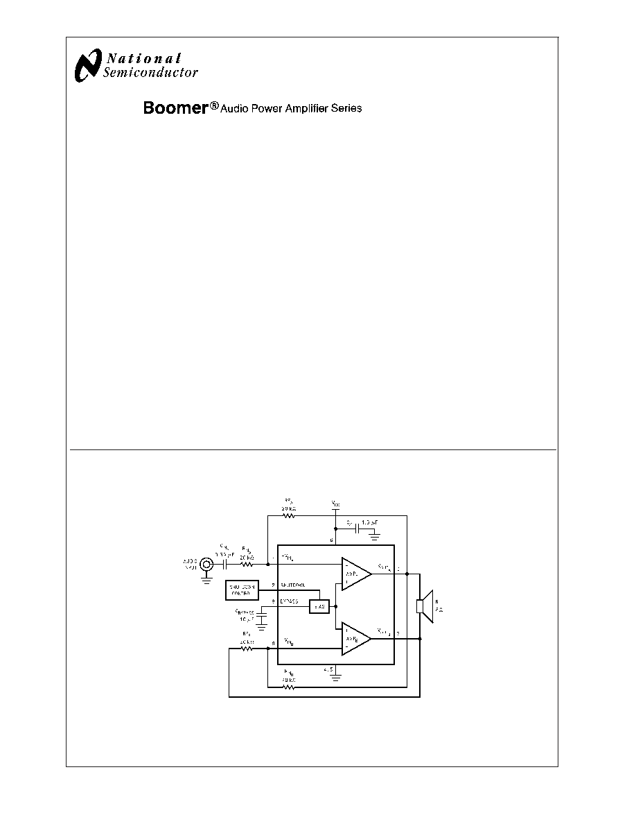
Typical Application
Boomer
�
is a registered trademark of National Semiconductor Corporation.
20047078
FIGURE 1. Typical Bridge-Tied-Load (BTL) Audio Amplifier Application Circuit
July 2003
7.5W
Mono-BTL
or
3.1W
Stereo
Audio
Power
Amplifier
� 2003 National Semiconductor Corporation
DS200470
www.national.com
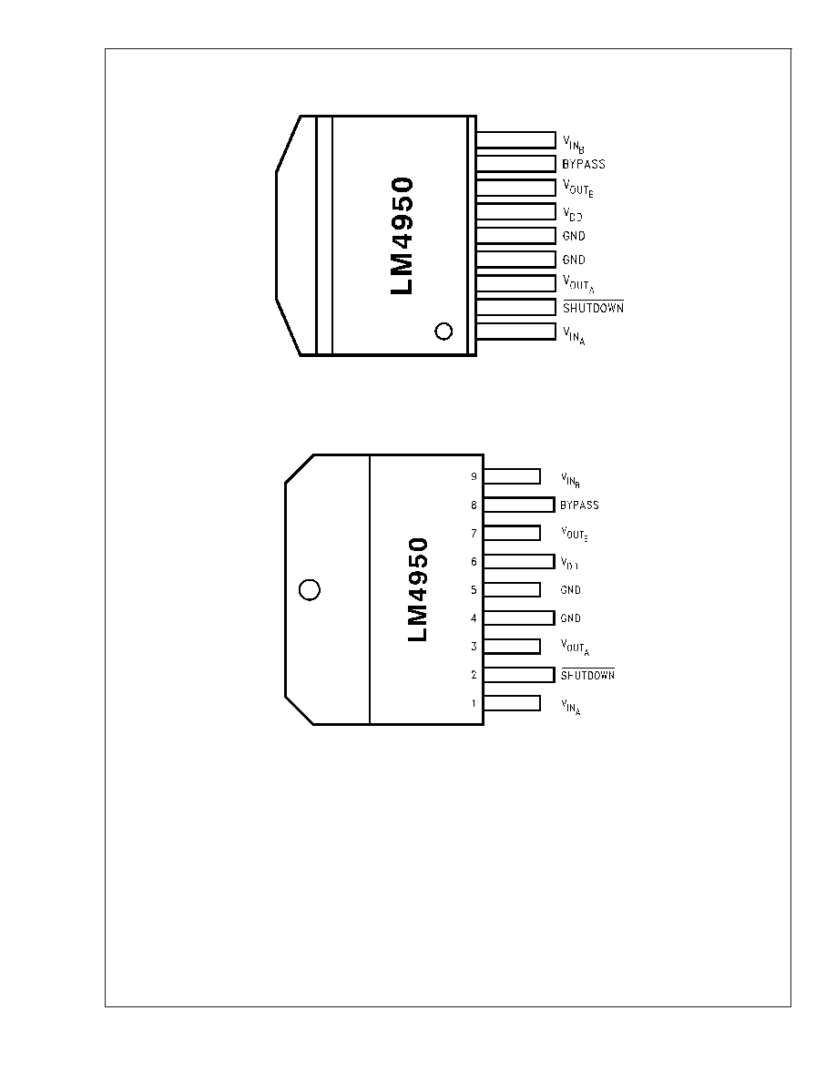
Connection Diagrams
Plastic Package, TO-263
20047070
Top View
Order Number LM4950TS
See NS Package Number TS9A
Plastic Package, TO-220
20047071
Top View
Order Number LM4950TA
See NS Package Number TA09A
LM4950
www.national.com
2
Absolute Maximum Ratings
(Notes 1,
2)
If Military/Aerospace specified devices are required,
please contact the National Semiconductor Sales Office/
Distributors for availability and specifications.
Supply Voltage (pin 6, referenced
to GND, pins 4 and 5)
18.0V
Storage Temperature
-65�C to +150�C
Input Voltage
pins 3 and 7
-0.3V to V
DD
+ 0.3V
pins 1, 2, 8, and 9
-0.3V to 9.5V
Power Dissipation (Note 3)
Internally limited
ESD Susceptibility (Note 4)
2000V
ESD Susceptibility (Note 5)
200V
Junction Temperature
150�C
Thermal Resistance
JC
(TS)
4�C/W
JA
(TS) (Note 3)
20�C/W
JC
(TA)
4�C/W
JA
(TA) (Note 3)
20�C/W
Operating Ratings
Temperature Range
T
MIN
T
A
T
MAX
-40�C
T
A
85�C
Supply Voltage
9.6V
V
DD
16V
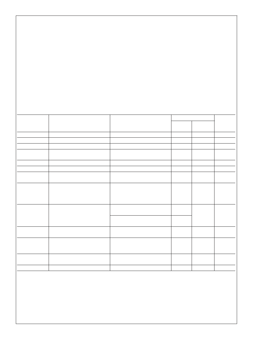
Electrical Characteristics V
DD
= 12V
(Notes 1, 2)
The following specifications apply for V
DD
= 12V, A
V
= 0dB (SE) or 6dB (BTL) unless otherwise specified. Limits apply for T
A
=
25�C.
Symbol
Parameter
Conditions
LM4950
Units
(Limits)
Typical
(Note 6)
Limit
(Notes 7, 8)
I
DD
Quiescent Power Supply Current
V
IN
= 0V, I
O
= 0A, No Load
16
30
mA (max)
I
SD
Shutdown Current
V
SHUTDOWN
= GND (Note 9)
40
80
�A (max)
V
OS
Offset Voltage
V
IN
= 0V, RL = 8
5
30
mV (max)
V
SDIH
Shutdown Voltage Input High
2.0
V
DD
/2
V (min)
V (max)
V
SDIL
Shutdown Voltage Input Low
0.4
V (max)
T
WU
Wake-up Time
C
B
= 10�F
440
ms
TSD
Thermal Shutdown Temperature
170
150
190
�C (min)
�C (max)
P
O
Output Power
f = 1kHz
R
L
= 4
SE, Single Channel,
THD+N = 1%
R
L
= 8
BTL, THD+N = 10%
3.1
7.5
3.0
W (min)
THD+N
Total Harmomic Distortion + Noise
P
O
= 2.5Wrms; f = 1kHz;
R
L
= 4
SE
0.05
%
P
O
= 2.5Wrms; A
V
= 10; f = 1kHz;
R
L
= 4
, SE
0.14
e
OS
Output Noise
A-Weighted Filter, V
IN
= 0V,
Input Referred
10
�V
X
TALK
Channel Separation
f
IN
= 1kHz, P
O
= 1W, SE Mode
R
L
= 8
R
L
= 4
76
70
dB
PSRR
Power Supply Rejection Ratio
V
RIPPLE
= 200mV
p-p
, f = 1kHz,
R
L
= 8
, BTL
70
56
dB (min)
I
OL
Output Current Limit
V
IN
= 0V, R
L
= 500m
5
A
Note 1: All voltages are measured with respect to the GND pin, unless otherwise specified.
Note 2: Absolute Maximum Ratings indicate limits beyond which damage to the device may occur. Operating Ratings indicate conditions for which the device is
functional, but do not guarantee specific performance limits. Electrical Characteristics state DC and AC electrical specifications under particular test conditions which
guarantee specific performance limits. This assumes that the device is within the Operating Ratings. Specifications are not guaranteed for parameters where no limit
is given, however, the typical value is a good indication of device performance.
Note 3: The maximum power dissipation must be derated at elevated temperatures and is dictated by T
JMAX
,
JA
, and the ambient temperature, T
A
. The maximum
allowable power dissipation is P
DMAX
= (T
JMAX
- T
A
) /
JA
or the given in Absolute Maximum Ratings, whichever is lower. For the LM4950 typical application (shown
in Figure 1) with V
DD
= 12V, R
L
= 4
stereo operation the total power dissipation is 3.65W.
JA
= 20�C/W for both TO263 and TO220 packages mounted to 16in
2
heatsink surface area.
Note 4: Human body model, 100pF discharged through a 1.5 k
resistor.
Note 5: Machine Model, 220pF�240pF discharged through all pins.
LM4950
www.national.com
3
Electrical Characteristics V
DD
= 12V
(Notes 1, 2) (Continued)
Note 6: Typicals are measured at 25�C and represent the parametric norm.
Note 7: Limits are guaranteed to National's AOQL (Average Outgoing Quality Level).
Note 8: Datasheet min/max specification limits are guaranteed by design, test, or statistical analysis.
Note 9: Shutdown current is measured in a normal room environment. The Shutdown pin should be driven as close as possible to GND for minimum shutdown
current.
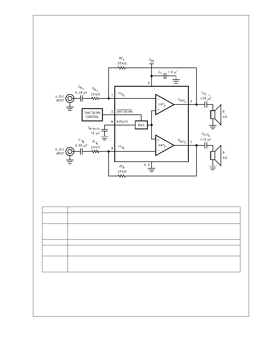
External Components Description
Refer to (Figure 1.)
Components
Functional Description
1. R
IN
This is the inverting input resistance that, along with R
F
, sets the closed-loop gain. Input resistance R
IN
and input capacitance C
IN
form a high pass filter. The filter's cutoff frequency is f
c
= 1/(2
R
IN
C
IN
).
2. C
IN
This is the input coupling capacitor. It blocks DC voltage at the amplifier's inverting input. C
IN
and R
IN
create a highpass filter. The filter's cutoff frequency is f
C
= 1/(2
R
IN
C
IN
). Refer to the SELECTING
EXTERNAL COMPONENTS, for an explanation of determining C
IN
's value.
3. R
F
This is the feedback resistance that, along with R
i
, sets closed-loop gain.
4. C
S
The supply bypass capacitor. Refer to the POWER SUPPLY BYPASSING section for information about
properly placing, and selecting the value of, this capacitor.
5. C
BYPASS
This capacitor filters the half-supply voltage present on the BYPASS pin. Refer to the Application section,
SELECTING EXTERNAL COMPONENTS, for information about properly placing, and selecting the
value of, this capacitor.
20047072
FIGURE 2. Typical Stereo Single-Ended (SE) Audio Amplifier Application Circuit
LM4950
www.national.com
4
Typical Performance Characteristics
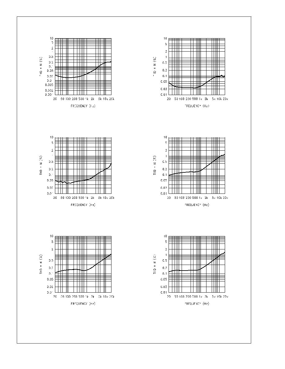
THD+N vs Frequency
THD+N vs Frequency
200470B2
V
DD
= 12V, R
L
= 8
,
BTL operation, P
OUT
= 1W
200470B3
V
DD
= 12V, R
L
= 8
,
BTL operation, P
OUT
= 3W
THD+N vs Frequency
THD+N vs Frequency
200470B4
V
DD
= 12V, R
L
= 8
,
BTL operation, P
OUT
= 5W
200470D5
V
DD
= 12V, R
L
= 8
,
BTL operation, BTLA
V
= 20, P
OUT
= 1W
THD+N vs Frequency
THD+N vs Frequency
200470D4
V
DD
= 12V, R
L
= 8
,
BTL operation, BTLA
V
= 20, P
OUT
= 3W
200470D6
V
DD
= 12V, R
L
= 8
,
BTL operation, BTLA
V
= 20, P
OUT
= 5W
LM4950
www.national.com
5