LM4951
Wide Voltage Range 1.8 Watt Audio Amplifier
General Description
The LM4951 is an audio power amplifier primarily designed
for demanding applications in Portable Handheld devices. It
is capable of delivering 1.8W mono BTL to an 8
load,
continuous average power, with less than 1% distortion
(THD+N) from a 7.5V
DC
power supply.
Boomer audio power amplifiers were designed specifically to
provide high quality output power with a minimal amount of
external components. The LM4951 does not require boot-
strap capacitors, or snubber circuits.
The LM4951 features a low-power consumption active-low
shutdown mode. Additionally, the LM4951 features an inter-
nal thermal shutdown protection mechanism.
The LM4951 contains advanced pop & click circuitry that
eliminates noises which would otherwise occur during
turn-on and turn-off transitions.
The LM4951 is unity-gain stable and can be configured by
external gain-setting resistors.
Key Specifications
j
Wide Voltage Range
2.7V to 9V
j
Quiescent Power Supply Current
(V
DD
= 7.5V)
2.5mA (typ)
j
Power Output BTL at 7.5V,
1% THD
1.8W (typ)
j
Shutdown Current
0.01�A (typ)
j
Fast Turn on Time
25mS (typ)
Features
n
Pop & click circuitry eliminates noise during turn-on and
turn-off transitions
n
Low current, active-low shutdown mode
n
Low quiescent current
n
Thermal shutdown protection
n
Unity-gain stable
n
External gain configuration capability
Applications
n
Portable Handheld Devices up to 9V
n
Cell Phone
n
PDA
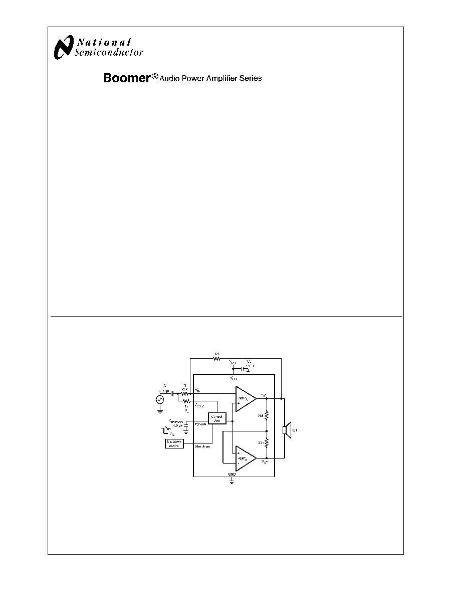
Typical Application
Boomer
�
is a registered trademark of National Semiconductor Corporation.
200942F4
* R
C
is needed for over/under voltage protection. If inputs are less than V
DD
+0.3V and greater than �0.3V, and if inputs are
disabled when in shutdown mode, then R
C
may be shorted.
FIGURE 1. Typical Bridge-Tied-Load (BTL) Audio Amplifier Application Circuit
November 2005
LM4951
W
ide
V
oltage
Range
1.8
W
att
Audio
Amplifier
� 2005 National Semiconductor Corporation
DS200942
www.national.com
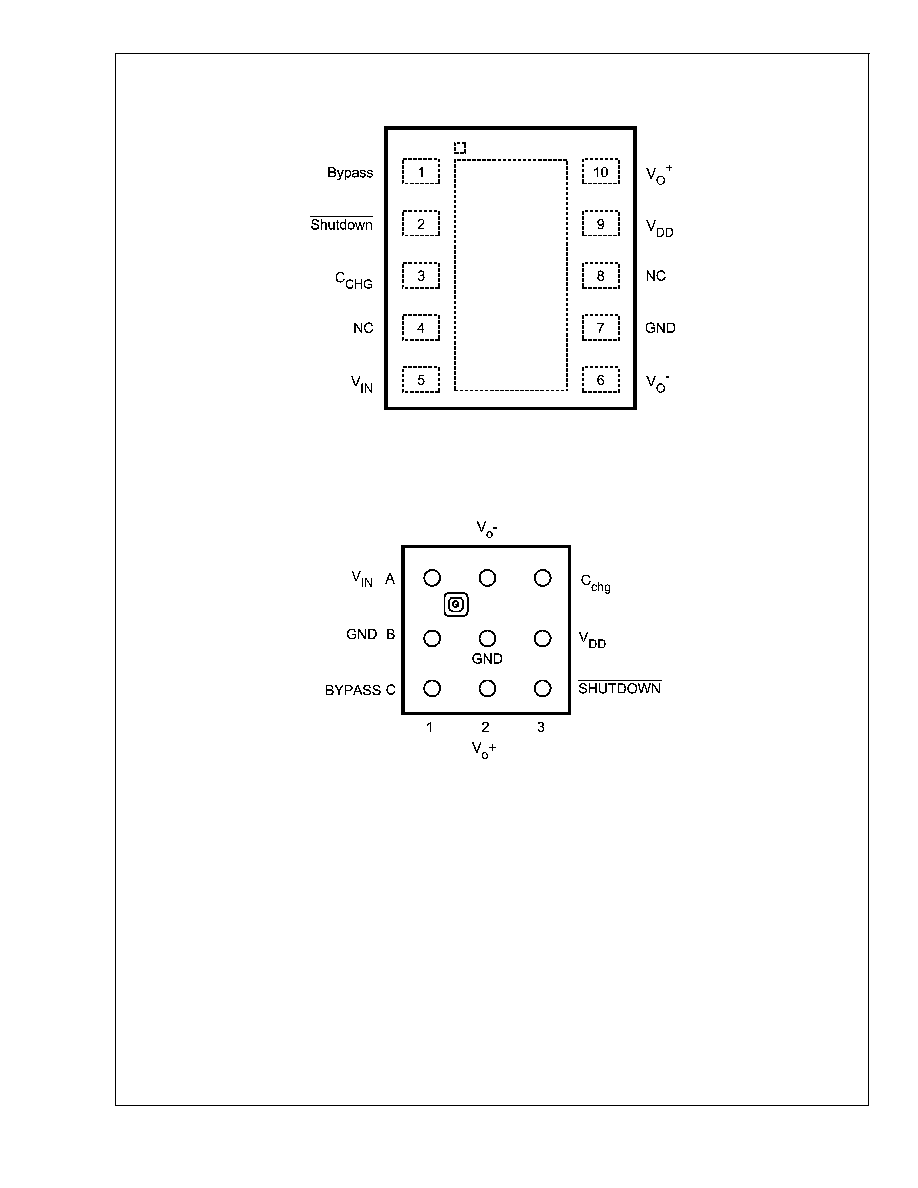
Connection Diagrams
SD Package
20094229
Top View
Order Number LM4951SD
See NS Package Number SDC10A
9 Bump micro SMD Package
20094228
Top View
Order Number LM4951TL, TLX
See NS Package Number TLA09ZZA
* DAP can either be soldered to GND or left floating.
LM4951
www.national.com
2
Absolute Maximum Ratings
(Notes 1, 2)
If Military/Aerospace specified devices are required,
please contact the National Semiconductor Sales Office/
Distributors for availability and specifications.
Supply Voltage
9.5V
Storage Temperature
-65�C to +150�C
Input Voltage
-0.3V to V
DD
+ 0.3V
Power Dissipation (Note 3)
Internally limited
ESD Susceptibility (Note 4)
2000V
ESD Susceptibility (Note 5)
200V
Junction Temperature
150�C
Thermal Resistance
JA
(LLP) (Note 3)
73�C/W
See AN-1187 'Leadless
Leadframe Packaging (LLP).'
Operating Ratings
Temperature Range
T
MIN
T
A
T
MAX
-40�C
T
A
+85�C
Supply Voltage
2.7V
V
DD
9V
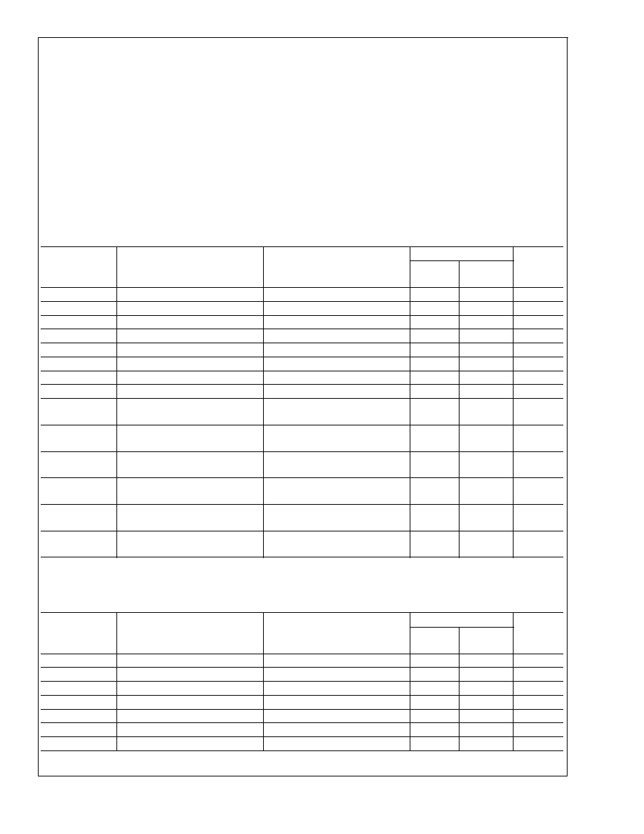
Electrical Characteristics V
DD
= 7.5V
(Notes 1, 2)
The following specifications apply for V
DD
= 7.5V, A
V-BTL
= 6dB, R
L
= 8
unless otherwise specified. Limits apply for T
A
=
25�C.
Symbol
Parameter
Conditions
LM4951
Units
(Limits)
Typical
(Note 6)
Limit
(Notes 7, 8)
I
DD
Quiescent Power Supply Current
V
IN
= 0V, I
O
= 0A,RL = 8
2.5
4.5
mA (max)
I
SD
Shutdown Current
V
SHUTDOWN
= GND (Note 9)
0.01
5
�A (max)
V
OS
Offset Voltage
5
30
mV (max)
V
SDIH
Shutdown Voltage Input High
1.2
V (min)
V
SDIL
Shutdown Voltage Input Low
0.4
V (max)
Rpulldown
Pulldown Resistor on S/D
75
45
k
(min)
T
WU
Wake-up Time
C
B
= 1.0�F
25
ms
Tsd
Shutdown time
C
B
= 1.0�F
10
ms (max)
TSD
Thermal Shutdown Temperature
170
150
190
�C (min)
�C (max)
P
O
Output Power
THD = 1% (max); f = 1kHz
R
L
= 8
Mono BTL
1.8
1.5
W (min)
THD+N
Total Harmomic Distortion + Noise
P
O
= 600mWrms; f = 1kHz
A
V-BTL
= 6dB
0.07
0.5
% (max)
THD+N
Total Harmomic Distortion + Noise
P
O
= 600mWrms; f = 1kHz
A
V-BTL
= 26dB
0.35
%
e
OS
Output Noise
A-Weighted Filter, R
i
= R
f
= 20k
Input Referred, Note 10
10
�V
PSRR
Power Supply Rejection Ratio
V
RIPPLE
= 200mV
p-p
, f = 217Hz,
C
B
= 1.0�F, Input Referred
66
56
dB (min)
Electrical Characteristics V
DD
= 3.3V
(Notes 1, 2)
The following specifications apply for V
DD
= 3.3V, A
V-BTL
= 6dB, R
L
= 8
unless otherwise specified. Limits apply for T
A
=
25�C.
Symbol
Parameter
Conditions
LM4951
Units
(Limits)
Typical
(Note 6)
Limit
(Notes 7, 8)
I
DD
Quiescent Power Supply Current
V
IN
= 0V, I
O
= 0A,RL = 8
2.5
4.5
mA (max)
I
SD
Shutdown Current
V
SHUTDOWN
= GND (Note 9)
0.01
2
�A (max)
V
OS
Offset Voltage
3
30
mV (max)
V
SDIH
Shutdown Voltage Input High
1.2
V (min)
V
SDIL
Shutdown Voltage Input Low
0.4
V (max)
T
WU
Wake-up Time
C
B
= 1.0�F
25
ms (max)
Tsd
Shutdown time
C
B
= 1.0�F
10
ms (max)
LM4951
www.national.com
3
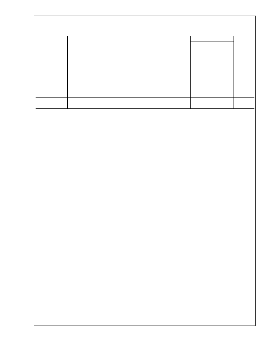
Electrical Characteristics V
DD
= 3.3V
(Notes 1, 2) (Continued)
The following specifications apply for V
DD
= 3.3V, A
V-BTL
= 6dB, R
L
= 8
unless otherwise specified. Limits apply for T
A
=
25�C.
Symbol
Parameter
Conditions
LM4951
Units
(Limits)
Typical
(Note 6)
Limit
(Notes 7, 8)
P
O
Output Power
THD = 1% (max); f = 1kHz
R
L
= 8
Mono BTL
280
230
W (min)
THD+N
Total Harmomic Distortion + Noise1 P
O
= 100mWrms; f = 1kHz
A
V-BTL
= 6dB
0.07
0.5
% (max)
THD+N
Total Harmomic Distortion + Noise1 P
O
= 100mWrms; f = 1kHz
A
V-BTL
= 26dB
0.35
%
e
OS
Output Noise
A-Weighted Filter, R
i
= R
f
= 20k
Input Referred, Note 10
10
�V
PSRR
Power Supply Rejection Ratio
V
RIPPLE
= 200mV
p-p
, f = 217Hz,
C
B
= 1�F, Input Referred
71
61
dB (min)
Note 1: All voltages are measured with respect to the GND pin, unless otherwise specified.
Note 2: Absolute Maximum Ratings indicate limits beyond which damage to the device may occur. Operating Ratings indicate conditions for which the device is
functional, but do not guarantee specific performance limits. Electrical Characteristics state DC and AC electrical specifications under particular test conditions which
guarantee specific performance limits. This assumes that the device is within the Operating Ratings. Specifications are not guaranteed for parameters where no limit
is given, however, the typical value is a good indication of device performance.
Note 3: The maximum power dissipation must be derated at elevated temperatures and is dictated by T
JMAX
,
JA
, and the ambient temperature, T
A
. The maximum
allowable power dissipation is P
DMAX
= (T
JMAX
- T
A
) /
JA
or the given in Absolute Maximum Ratings, whichever is lower. For the LM4951 typical application (shown
in Figure 1) with V
DD
= 7.5V, R
L
= 8
mono-BTL operation the max power dissipation is 1.42W.
JA
= 73�C/W.
Note 4: Human body model, 100pF discharged through a 1.5k
resistor.
Note 5: Machine Model, 220pF�240pF discharged through all pins.
Note 6: Typicals are measured at 25�C and represent the parametric norm.
Note 7: Limits are guaranteed to National's AOQL (Average Outgoing Quality Level).
Note 8: Datasheet min/max specification limits are guaranteed by design, test, or statistical analysis.
Note 9: Shutdown current is measured in a normal room environment. The Shutdown pin should be driven as close as possible to GND for minimum shutdown
current.
Note 10: Noise measurements are dependent on the absolute values of the closed loop gain setting resistors (input and feedback resistors).
LM4951
www.national.com
4
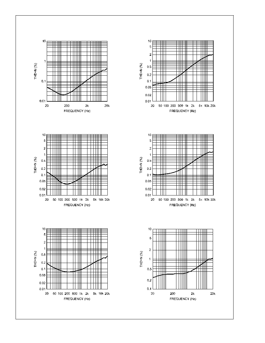
Typical Performance Characteristics
THD+N vs Frequency
V
DD
= 3.3V, P
O
= 100mW, A
V
= 6dB
THD+N vs Frequency
V
DD
= 3.3V, P
O
= 100mW, A
V
= 26dB
200942F9
20094202
THD+N vs Frequency
V
DD
= 5V, P
O
= 400mW, A
V
= 6dB
THD+N vs Frequency
V
DD
= 5V, P
O
= 400mW, A
V
= 26dB
20094203
20094204
THD+N vs Frequency
V
DD
= 7.5V, P
O
= 600mW, A
V
= 6dB
THD+N vs Frequency
V
DD
= 7.5V, P
O
= 600mW, A
V
= 26dB
20094205
200942G0
LM4951
www.national.com
5