 | –≠–ª–µ–∫—Ç—Ä–æ–Ω–Ω—ã–π –∫–æ–º–ø–æ–Ω–µ–Ω—Ç: LM4953 | –°–∫–∞—á–∞—Ç—å:  PDF PDF  ZIP ZIP |
LM4953
Ground-Referenced, Ultra Low Noise, Ceramic Speaker
Driver
General Description
The LM4953 is an audio power amplifier designed for driving
Ceramic Speaker in portable applications. When powered by
a 3.6V supply, it is capable of forcing 12.6Vpp across a 2µF
+ 30
bridge-tied-load (BTL) with less than 1% THD+N.
Boomer audio power amplifiers were designed specifically to
provide high quality output power with a minimal amount of
external components. The LM4953 does not require boot-
strap capacitors, or snubber circuits. Therefore it is ideally
suited for display applications requiring high power and mini-
mal size.
The LM4953 features a low-power consumption shutdown
mode. Additionally, the LM4953 features an internal thermal
shutdown protection mechanism.
The LM4953 contains advanced pop & click circuitry that
eliminates noises which would otherwise occur during
turn-on and turn-off transitions.
The LM4953 is unity-gain stable and can be configured by
external gain-setting resistors.
Key Specifications
j
Quiescent Power Supply Current (V
dd
= 3V) 7mA(typ)
j
BTL Voltage Swing
(2µF+30
load, 1% THD+N,
V
dd
= 3.6V)
12.6V
pp
(typ)
j
Shutdown Current
1µA (max)
Features
n
Pop & click circuitry eliminates noise during turn-on and
turn-off transitions
n
Low, 1µA (max) shutdown current
n
Low, 7mA (typ) quiescent current
n
12.6Vpp mono BTL output, load = 2µF+ 30
n
Thermal shutdown
n
Unity-gain stable
n
External gain configuration capability
Applications
n
Cellphone
n
PDA
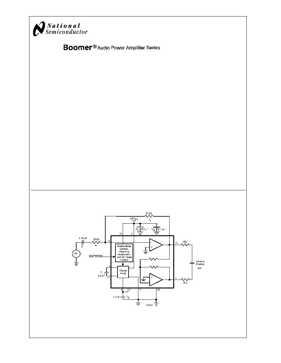
Typical Application
Boomer
Æ
is a registered trademark of National Semiconductor Corporation.
20142168
FIGURE 1. Typical Application Circuit
September 2005
LM4953
Ground-Referenced,
Ultra
Low
Noise,
Ceramic
Speaker
Driver
© 2005 National Semiconductor Corporation
DS201421
www.national.com
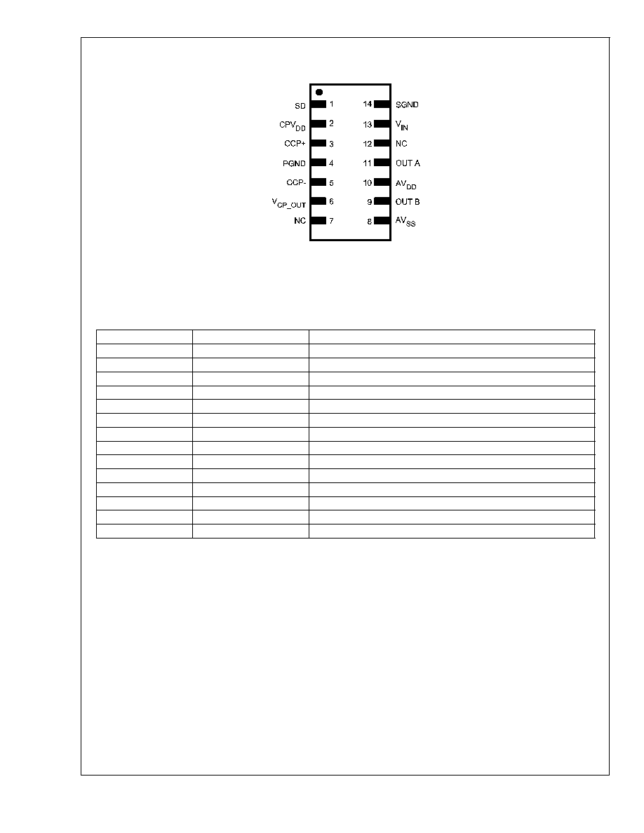
Connection Diagram
LLP Package
20142101
Top View
Order Number LM4953SD
See NS Package Number SDA14A
Pin Descriptions
Pin
Name
Function
1
SD
Active Low Shutdown
2
CP
VDD
Charge Pump Power Supply
3
CCP+
Positive Terminal - Charge Pump Flying Capacitor
4
PGND
Power Ground
5
CCP-
Negative Terminal - Charge Pump Flying Capacitor
6
V
CP_OUT
Charge Pump Output
7
NC
No Connect
8
AV
SS
Negative Power Supply - Amplifier
9
OUT B
Output B
10
AV
DD
Positive Power Supply - Amplifier
11
OUT A
Output A
12
NC
No Connect
13
V
IN
Signal Input
14
SGND
Signal Ground
LM4953
www.national.com
2
Absolute Maximum Ratings
(Notes 1, 2)
If Military/Aerospace specified devices are required,
please contact the National Semiconductor Sales Office/
Distributors for availability and specifications.
Supply Voltage (V
DD
)
4.5V
Storage Temperature
-65∞C to +150∞C
Input Voltage
-0.3V to V
DD
+ 0.3V
Power Dissipation (Note 3)
Internally Limited
ESD Susceptibility (Note 4)
2000V
ESD Susceptibility (Note 5)
200V
Junction Temperature
150∞C
Thermal Resistance
See AN-1187 'Leadless Leadframe Packaging (LLP).'
Operating Ratings
Temperature Range
T
MIN
T
A
T
MAX
-40∞C
T
A
85∞C
Supply Voltage (V
DD
)
1.6V
V
DD
4.2V
Electrical Characteristics V
DD
= 3.6V
The following specifications apply for V
DD
= 3.6V, A
V-BTL
= 6dB, Z
L
= 2µF+30
unless otherwise specified. Limits apply to T
A
=
25∞C. See Figure 1.
Symbol
Parameter
Conditions
LM4953
Units (Limits)
Typ
(Note 6)
Limit
(Notes 7, 8)
I
DD
Quiescent Power Supply
Current
V
IN
= 0, R
LOAD
= 2µF+30
8
TBD
mA (max)
I
standby
Quiescent Power Supply
Current Auto Standby Mode
V
IN
= 0, Z
LOAD
= 2µF+30
2.7
mA
I
SD
Shutdown Current
V
SD
= GND
0.1
1
µA (max)
V
SDIH
Shutdown Voltage Input High
SD1
SD2
0.7*CPVdd
V (min)
V
SDIL
Shutdown Voltage Input Low
SD1
SD2
0.3*CPVdd
V (max)
T
WU
Wake-up Time
125
µsec
V
OS
Output Offset Voltage
1
10
mV (max)
V
OUT
Output Voltage Swing
THD = 1% (max); f = 1kHz
R
L
= 2µF+30
, Mono BTL
12.6
Vpp
THD+N
Total Harmonic Distortion +
Noise
V
OUT
= 6Vp-p, f
IN
= 1kHz
0.02
%
OS
Output Noise
A-Weighted Filter, V
IN
= 0V
15
µV
PSRR
Power Supply Rejection
Ratio
V
RIPPLE
= 200mVp-p, f = 217Hz,
Input Referred
67
dB
V
RIPPLE
= 200mVp-p, f = 1kHz,
Input Referred
65
dB
SNR
Signal-to-Noise Ratio
Z
L
= 2µF+30
, V
OUT
= 6Vp-p
105
dB
Electrical Characteristics V
DD
= 3.0V
The following specifications apply for V
DD
= 3.0V, A
V-BTL
= 6dB, Z
L
= 2µF+30
unless otherwise specified. Limits apply to T
A
=
25∞C. See Figure 1.
Symbol
Parameter
Conditions
LM4953
Units (Limits)
Typ
(Note 6)
Limit
(Notes 7, 8)
I
DD
Quiescent Power Supply
Current
V
IN
= 0, Z
LOAD
= 2µF+30
7
10
mA (max)
I
standby
Quiescent Power Supply
Current Auto Standby Mode
V
IN
= 0, Z
LOAD
= 2µF+30
2.3
mA
I
SD
Shutdown Current
V
SD-LC
= V
SD-RC
= GND
0.1
1
µA (max)
V
SDIH
Shutdown Voltage Input High
SD1
SD2
0.7*CPVdd
V (min)
LM4953
www.national.com
3
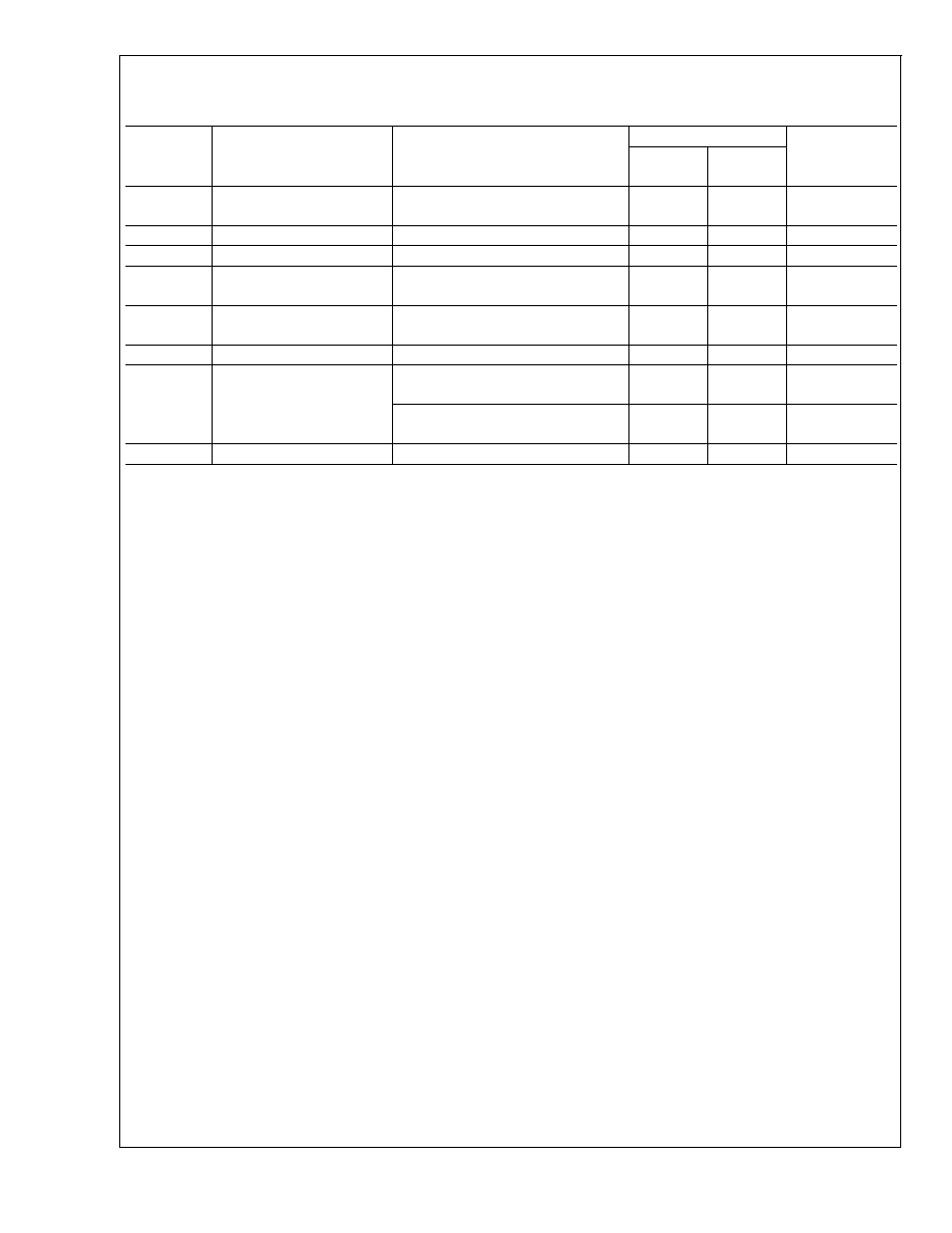
Electrical Characteristics V
DD
= 3.0V
(Continued)
The following specifications apply for V
DD
= 3.0V, A
V-BTL
= 6dB, Z
L
= 2µF+30
unless otherwise specified. Limits apply to T
A
=
25∞C. See Figure 1.
Symbol
Parameter
Conditions
LM4953
Units (Limits)
Typ
(Note 6)
Limit
(Notes 7, 8)
V
SDIL
Shutdown Voltage Input Low
SD1
SD2
0.3*CPVdd
V (max)
T
WU
Wake-up Time
125
µsec
V
OS
Output Offset Voltage
1
10
mV (max)
V
OUT
Output Voltage Swing
THD = 1% (max); f = 1kHz
Z
L
= 2µF+30
, Mono BTL
10.2
Vpp
THD+N
Total Harmonic Distortion +
Noise
V
OUT
= 8.5Vp-p, f
IN
= 1kHz
0.02
%
OS
Output Noise
A-Weighted Filter, V
IN
= 0V
15
µV
PSRR
Power Supply Rejection
Ratio
V
RIPPLE
= 200mVp-p, f = 217Hz,
Input Referred
73
dB
V
RIPPLE
= 200mVp-p, f = 1kHz,
Input Referred
68
dB
SNR
Signal-to-Noise Ratio
Z
L
= 2µF+30
, V
OUT
= 8.5Vp-p
105
dB
Note 1: All voltages are measured with respect to the GND pin unless otherwise specified.
Note 2: Absolute Maximum Ratings indicate limits beyond which damage to the device may occur. Operating Ratings indicate conditions for which the device is
functional but do not guarantee specific performance limits. Electrical Characteristics state DC and AC electrical specifications under particular test conditions that
guarantee specific performance limits. This assumes that the device is within the Operating Ratings. Specifications are not guaranteed for parameters where no limit
is given; however, the typical value is a good indication of device performance.
Note 3: The maximum power dissipation must be derated at elevated temperatures and is dictated by T
JMAX
,
JA
, and the ambient temperature, T
A
. The maximum
allowable power dissipation is P
DMAX
= (T
JMAX
≠ T
A
)/
JA
or the number given in Absolute Maximum Ratings, whichever is lower. For the LM4xxx typical application
(shown in Figure 1) with V
DD
= yyV, R
L
= 2µF+30
mono BTL operation the total power dissipation is xxxW.
JA
= 40∞C/W.
Note 4: Human body model, 100pF discharged through a 1.5k
resistor.
Note 5: Machine Model, 220pF-240pF discharged through all pins.
Note 6: Typicals are measured at 25∞C and represent the parametric norm.
Note 7: Limits are guaranteed to National's AOQL (Average Outgoing Quality Level).
Note 8: Datasheet min/max specification limits are guaranteed by design, test, or statistical analysis.
Note 9: If the product is in shutdown mode and V
DD
exceeds 3.6V (to a max of 4V V
DD
), then most of the excess current will flow through the ESD protection circuits.
If the source impedance limits the current to a max of 10mA, then the part will be protected. If the part is enabled when V
DD
is above 4V, circuit performance will
be curtailed or the part may be permanently damaged.
LM4953
www.national.com
4
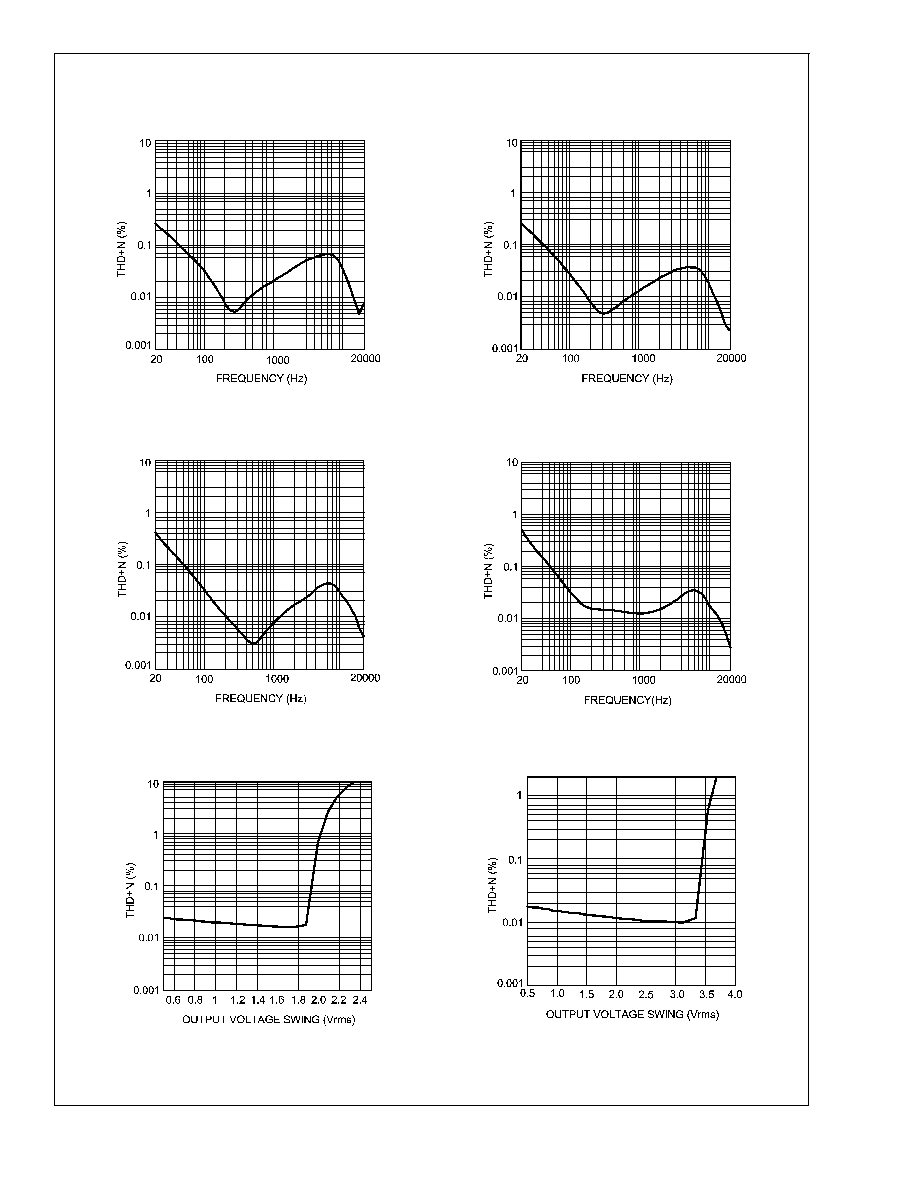
Typical Performance Characteristics
THD+N vs Frequency
V
DD
= 2V, V
O
= 2Vpp, Z
L
= 2µF+30
THD+N vs Frequency
V
DD
= 3V, V
O
= 6Vpp, Z
L
= 2µF+30
20142112
20142113
THD+N vs Frequency
V
DD
= 3.6V, V
O
= 8.5Vpp, Z
L
= 2µF+30
THD+N vs Frequency
V
DD
= 4.2V, V
O
= 10Vpp, Z
L
= 2µF+30
20142114
20142118
THD+N vs Output Voltage
V
DD
= 2V, f = 1kHz, Z
L
= 2µF+30
THD+N vs Output Voltage
V
DD
= 3V, f = 1kHz, Z
L
= 2µF+30
20142119
20142121
LM4953
www.national.com
5