LM4960
Piezoelectric Speaker Driver
General Description
The LM4960 utilizes a switching regulator to drive a dual
audio power amplifier. It delivers 24V
P-P
mono-BTL to a
ceramic speaker with less than 1.0% THD+N while operating
on a 3.0V power supply.
The LM4960's switching regulator is a current-mode boost
converter operating at a fixed frequency of 1.6MHz.
Boomer audio power amplifiers were designed specifically to
provide high quality output power with a minimal amount of
external components. The LM4960 does not require output
coupling capacitors or bootstrap capacitors, and therefore is
ideally suited for mobile phone and other low voltage appli-
cations where minimal power consumption is a primary re-
quirement.
The LM4960 features a low-power consumption externally
controlled micropower shutdown mode. Additionally, the
LM4960 features and internal thermal shutdown protection
mechanism along with a short circuit protection.
The LM4960 is unity-gain stable and can be configured by
external gain-setting resistors.
Key Specifications
n
V
OUT
@
V
DD
= 3.0 THD+N
1%
24V
P-P
(typ)
n
Power supply range
3.0 to 7V
n
Switching Frequency
1.6MHz (typ)
Features
n
Stereo BTL amplifier
n
Low current shutdown mode
n
"Click and pop" suppression circuitry
n
Low Quiescent current
n
Unity-gain stable audio amplifiers
n
External gain configuration capability
n
Thermal shutdown protection circuitry
n
Wide input voltage range (3.0V - 7V)
n
1.6MHz switching frequency
Applications
n
Mobile phone
n
PDA's
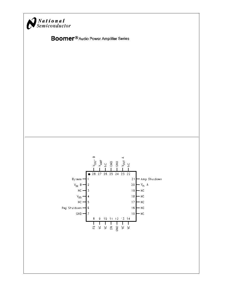
Connection Diagram
LM4960SQ
20076582
Top View
Order Number LM4960SQ
See NS Package Number
Boomer
�
is a registered trademark of National Semiconductor Corporation.
October 2004
LM4960
Piezoelectric
Speaker
Driver
� 2004 National Semiconductor Corporation
DS200765
www.national.com
Absolute Maximum Ratings
(Notes 1, 2)
If Military/Aerospace specified devices are required,
please contact the National Semiconductor Sales Office/
Distributors for availability and specifications.
Supply Voltage (V
DD
)
8.5V
Supply Voltage (V1)
(Pin 27 referred to GND)
18V
Storage Temperature
-65�C to +150�C
Input Voltage
-0.3V to V
DD
+ 0.3V
Power Dissipation (Note 3)
Internally limited
ESD Susceptibility (Note 4)
2000V
ESD Susceptibility (Note 5)
200V
Junction Temperature
150�C
Thermal Resistance
JA
(LLP)
�C/W
See AN-1187 'Leadless Leadframe Packaging (LLP).'
Operating Ratings
Temperature Range
T
MIN
T
A
T
MAX
-40�C
T
A
+85�C
Supply Voltage (V
DD
)
3.0V
V
DD
7V
Supply Voltage (V1)
9.6V
V
1
16V
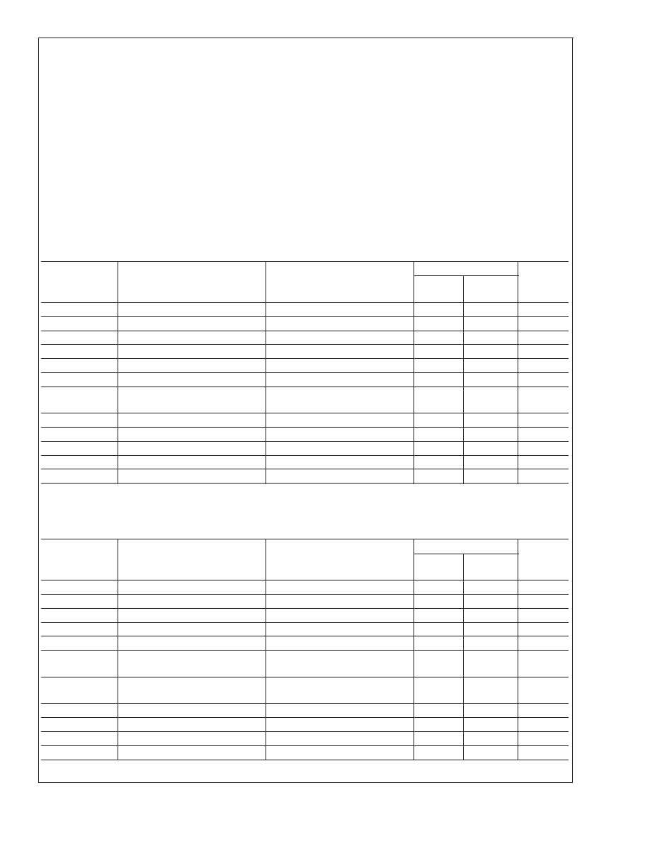
Electrical Characteristics V
DD
= 3.0V
(Notes 1, 2)
The following specifications apply for V
DD
= 3V, A
V
= 10, R
L
= 800nF+20
, V1 = 12V unless otherwise specified. Limits apply
for T
A
= 25�C.
Symbol
Parameter
Conditions
LM4960
Units
(Limits)
Typical
(Note 6)
Limit
(Notes 7, 8)
I
DD
Quiescent Power Supply Current
V
IN
= GND, No Load
85
150
mA (max)
I
SD
Shutdown Current
V
SHUTDOWN
= GND (Note 9)
30
100
�A (max)
V
OS
Output Offset Voltage
5
40
mV (max)
V
SDIH
Shutdown Voltage Input High
2
V (max)
V
SDIL
Shutdown Voltage Input Low
0.4
V (min)
T
WU
Wake-up Time
C
B
= 0.22�F
50
ms
TSD
Thermal Shutdown Temperature
170
150
190
�C (min)
�C (max)
V
O
Output Voltage
THD = 1% (max); f = 1kHz
24
20
V
P-P
(min)
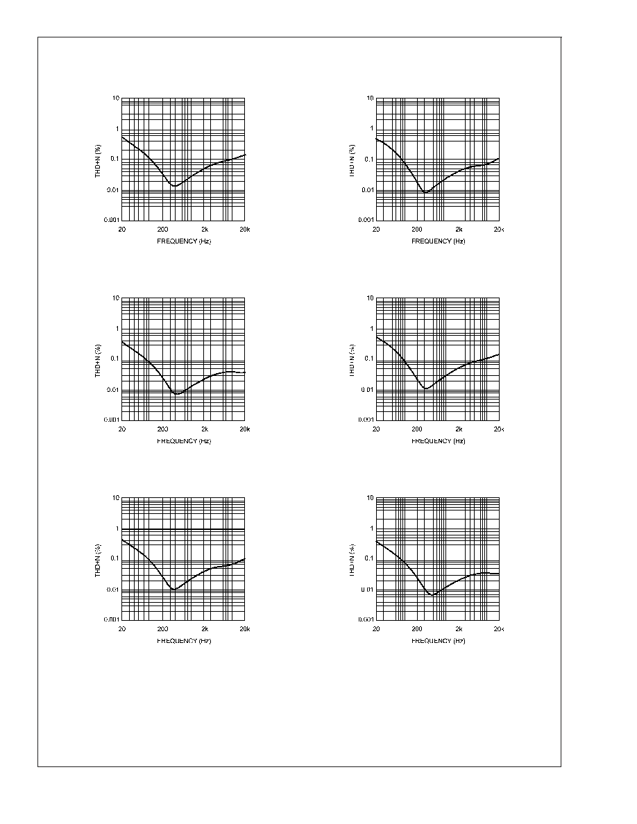
THD+N
Total Harmomic Distortion + Noise
V
O
= 3Wrms; f = 1kHz
0.04
%
e
OS
Output Noise
A-Weighted Filter, V
IN
= 0V
90
�V
PSRR
Power Supply Rejection Ratio
V
RIPPLE
= 200mV
p-p
, f = 1kHz
55
50
dB (min)
V
FB
Feedback Pin Reference Voltage
1.23
V (max)
Electrical Characteristics V
DD
= 5.0V
(Notes 1, 2)
The following specifications apply for V
DD
= 5V, A
V
= 10, R
L
= 800nF+20
unless otherwise specified. Limits apply for T
A
=
25�C.
Symbol
Parameter
Conditions
LM4960
Units
(Limits)
Typical
(Note 6)
Limit
(Notes 7, 8)
I
DD
Quiescent Power Supply Current
V
IN
= GND, No Load
45
mA (max)
I
SD
Shutdown Current
V
SHUTDOWN
= GND (Note 9)
55
100
�A (max)
V
SDIH
Shutdown Voltage Input High
2
V (max)
V
SDIL
Shutdown Voltage Input Low
0.4
V (min)
T
WU
Wake-up Time
C
B
= 0.22�F
50
s
TSD
Thermal Shutdown Temperature
170
150
190
�C (min)
�C (max)
V
O
Output Voltage
THD = 1% (max); f = 1kHz
R
L
= Ceramic Speaker
24
20
V
P-P
(min)
THD+N
Total Harmomic Distortion + Noise
V
O
= 3Wrms; f = 1kHz
0.04
%
e
OS
Output Noise
A-Weighted Filter, V
IN
= 0V
90
�V
PSRR
Power Supply Rejection Ratio
V
RIPPLE
= 200mV
p-p
, f = 1kHz
60
dB (min)
V
FB
Feedback Pin Reference Voltage
1.23
V (max)
Note 1: All voltages are measured with respect to the GND pin, unless otherwise specified.
LM4960
www.national.com
3

Electrical Characteristics V
DD
= 5.0V
(Notes 1, 2) (Continued)
Note 2: Absolute Maximum Ratings indicate limits beyond which damage to the device may occur. Operating Ratings indicate conditions for which the device is
functional, but do not guarantee specific performance limits. Electrical Characteristics state DC and AC electrical specifications under particular test conditions which
guarantee specific performance limits. This assumes that the device is within the Operating Ratings. Specifications are not guaranteed for parameters where no limit
is given, however, the typical value is a good indication of device performance.
Note 3: The maximum power dissipation must be derated at elevated temperatures and is dictated by T
JMAX
,
JA
, and the ambient temperature, T
A
. The maximum
allowable power dissipation is P
DMAX
= (T
JMAX
- T
A
) /
JA
or the given in Absolute Maximum Ratings, whichever is lower. For the LM4960 typical application (shown
in Figure 1) with V
DD
= 12V, R
L
= 4
stereo operation the total power dissipation is 3.65W.
JA
= 35�C/W.
Note 4: Human body model, 100pF discharged through a 1.5k
resistor.
Note 5: Machine Model, 220pF�240pF discharged through all pins.
Note 6: Typicals are measured at 25�C and represent the parametric norm.
Note 7: Limits are guaranteed to National's AOQL (Average Outgoing Quality Level).
Note 8: Datasheet min/max specification limits are guaranteed by design, test, or statistical analysis.
Note 9: Shutdown current is measured in a normal room environment. The Shutdown pin should be driven as close as possible to V
DD
for minimum shutdown
current.
LM4960
www.national.com
4