LM4961
Ceramic Speaker Driver
General Description
The LM4961 is an audio power amplifier primarily designed
for driving Ceramic Speaker for applications in Cell Phone
and PDAs. It integrates a boost converter, with variable
output voltage, with an audio power amplifier. It is capable of
driving 15V
p-p
in BTL mode to 2uF+ 30 ohms load, continu-
ous average power, with less than 1% distortion (THD+N)
from a 3.2V
DC
power supply.
Boomer audio power amplifiers were designed specifically to
provide high quality output power with a minimal number of
external components. The LM4961 does not require boot-
strap capacitors, or snubber circuits therefore it is ideally
suited for portable applications requiring high voltage output
to drive capacitive loads like Ceramic Speakers. The
LM4961 features a low-power consumption shutdown mode.
Additionally, the LM4961 features an internal thermal shut-
down protection mechanism.
The LM4961 contains advanced pop & click circuitry that
eliminates noises which would otherwise occur during
turn-on and turn-off transitions.
The LM4961 is unity-gain stable and can be configured by
external gain-setting resistors.
Key Specifications
n
Quiescent Power Supply Current
7mA (typ)
n
Voltage Swing in BTL at 1% THD
15Vp-p (typ)
n
Shutdown current
0.1µA (typ)
Features
n
Pop & click circuitry eliminates noise during turn-on and
turn-off transitions
n
Low current shutdown mode
n
Low quiescent current
n
Mono 15Vp-p BTL output, R
L
= 2µF+30
, f = 1kHz
n
Thermal shutdown protection
n
Unity-gain stable
n
External gain configuration capability
n
Including Band exchange SW
n
Including Leakage cut SW
Applications
n
Cellphone
n
PDA
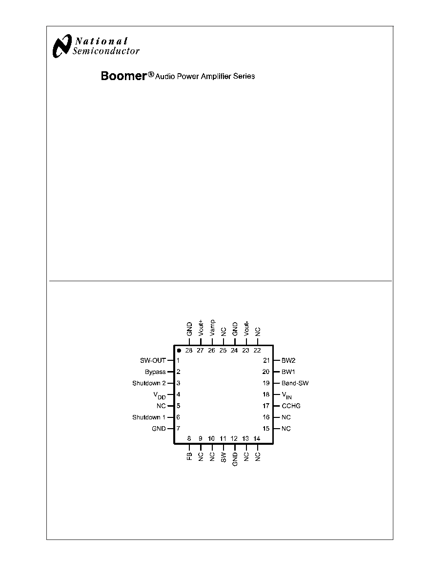
Connection Diagram
LM4961LQ (5x5)
20094084
Top View
Order Number LM4XXX
See NS Package Number
Boomer
Æ
is a registered trademark of National Semiconductor Corporation.
October 2004
LM4961
Ceramic
Speaker
Driver
© 2004 National Semiconductor Corporation
DS200940
www.national.com
Absolute Maximum Ratings
(Notes 1, 2)
If Military/Aerospace specified devices are required,
please contact the National Semiconductor Sales Office/
Distributors for availability and specifications.
Supply Voltage (V
dd
)
6.0V
Amplifier Supply Voltage (V
1
)
9.5V
Storage Temperature
-65∞C to +150∞C
Input Voltage
-0.3V to V
DD
+ 0.3V
Power Dissipation (Note 3)
Internally limited
ESD Susceptibility (Note 4)
2000V
ESD Susceptibility (Note 5)
200V
Junction Temperature
150∞C
Thermal Resistance
JA
(LLP)
66∞C/W
See AN-1187 'Leadless Leadframe Packaging (LLP).'
Operating Ratings
Temperature Range
T
MIN
T
A
T
MAX
-40∞C
T
A
+85∞C
Supply Voltage (V
DD
)
3.0V
<
V
DD
<
5.0V
Amplifier Supply Voltage (V
1
)
2.7V
<
V
1
<
9.0V
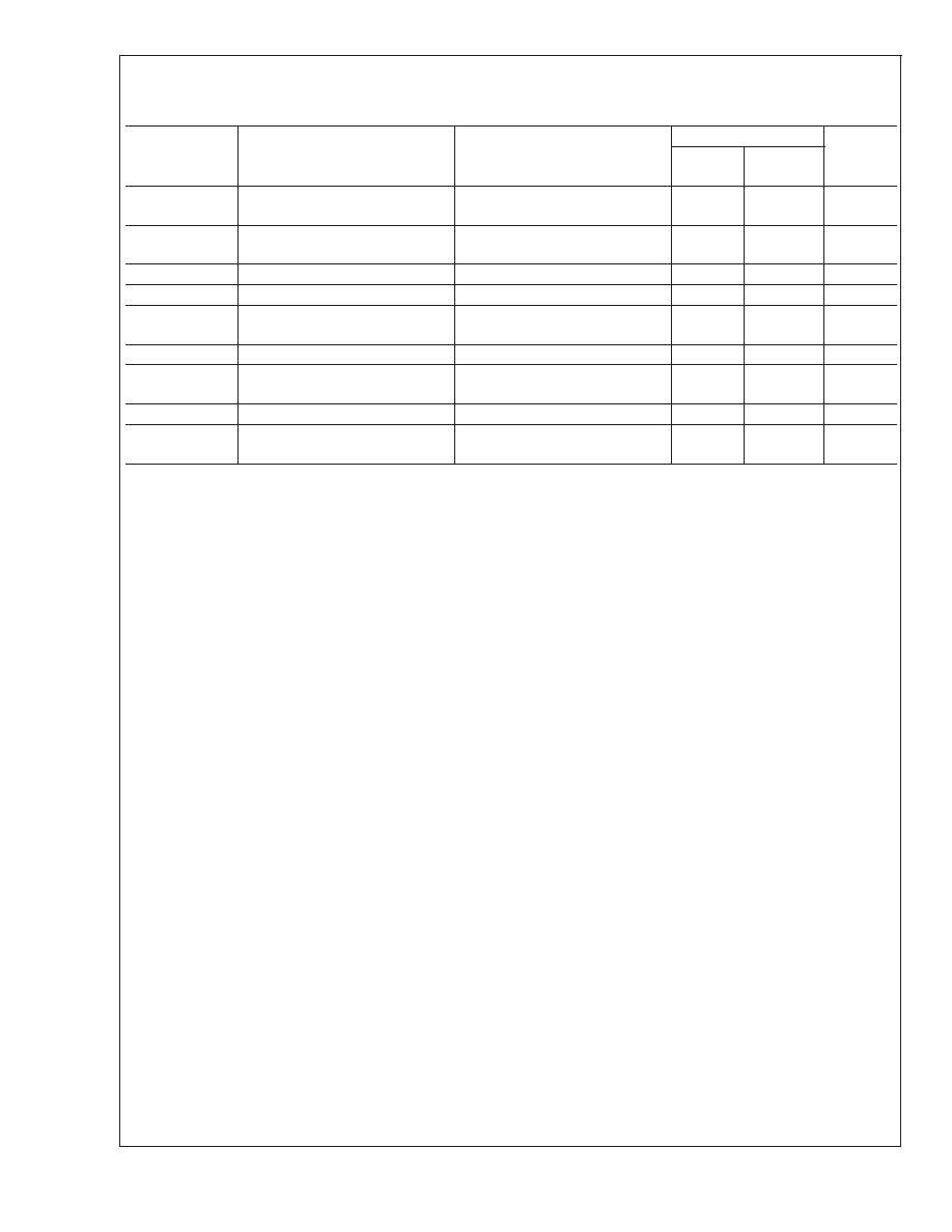
Electrical Characteristics V
DD
= 4.2V
The following specifications apply for V
DD
= 4.2V, A
V-BTL
= 26dB, R
L
= 2µF+30
, Cb = 1.0µF, Band-SW = V
DD
unless other-
wise specified. Limits apply for T
A
= 25∞C.
Symbol
Parameter
Conditions
LM4961
Units
(Limits)
Typical
(Note 6)
Limit
(Notes 7, 8)
I
DD
Quiescent Power Supply Current
V
IN
= 0V, No Load
Band-SW = V
DD
7
14
mA (max)
Iddrcv
Iq in receiver mode
V
IN
= 0V, No Load
Band-SW = GND
2
4
mA (max)
I
SD
Shutdown Current
V
SHUTDOWN1
= V
SHUTDOWN2
=
GND
Band-SW = GND (Note 9)
0.1
2.0
µA (max)
V
LH
Logic High Threshold Voltage
For Shutdown 1, Shutdown 2, and
Band-SW
1.5
V (min)
V
LL
Logic Low Threshold Voltage
For Shutdown 1, Shutdown 2, and
Band-SW
0.4
V (max)
R
PULLDOWN
Pulldown Resistor
For Shutdown 2 and Band-SW
70k
50k
(min)
TSD
Thermal Shutdown Temperature
125
∞C (min)
V
out
Output Voltage Swing
THD = 1%, f = 1kHz
R
L
= 2µF+30
Mono BTL
15
14
Vp-p (min)
THD+N
Total Harmomic Distortion + Noise
V
out
= 14Vp-p, f = 1kHz
0.05
1.0
% (max)
e
OS
Output Noise
A-Weighted Filter, V
IN
= 0V (Note
10)
115
µV
PSRR
Power Supply Rejection Ratio
V
RIPPLE
= 200mV
p-p
, f = 100Hz
80
65
dB (min)
Ron-sw-out
On Resistance on SW-Out
Band SW "High" Isink = 100µA
(Between pin 1 and pin 28)
170
220
(max)
Electrical Characteristics V
DD
= 3.2V
The following specifications apply for V
DD
= 3.2V, A
V-BTL
= 26dB, R
L
= 2µF+30
, Cb = 1.0µF, Band-SW = V
DD
unless other-
wise specified. Limits apply for T
A
= 25∞C.
Symbol
Parameter
Conditions
LM4961
Units
(Limits)
Typical
(Note 6)
Limit
(Notes 7, 8)
I
DD
Quiescent Power Supply Current
V
IN
= 0V, No Load
Band-SW = V
DD
9
15
mA (max)
Iddrcv
Iq in receiver mode
V
IN
= 0V, No Load
Band-SW = GND
2
4
mA (max)
I
SD
Shutdown Current
V
SHUTDOWN1
= V
SHUTDOWN2
=
GND
Band-SW = GND (Note 9)
0.1
2.0
µA (max)
LM4961
www.national.com
3
Electrical Characteristics V
DD
= 3.2V
(Continued)
The following specifications apply for V
DD
= 3.2V, A
V-BTL
= 26dB, R
L
= 2µF+30
, Cb = 1.0µF, Band-SW = V
DD
unless other-
wise specified. Limits apply for T
A
= 25∞C.
Symbol
Parameter
Conditions
LM4961
Units
(Limits)
Typical
(Note 6)
Limit
(Notes 7, 8)
V
LH
Logic High Threshold Voltage
For Shutdown 1, Shutdown 2, and
Band-SW
1.5
V (min)
V
LL
Logic Low Threshold Voltage
For Shutdown 1, Shutdown 2, and
Band-SW
0.4
V (max)
R
PULLDOWN
Pulldown Resistor
For Shutdown 2 and Band-SW
70k
50k
(min)
TSD
Thermal Shutdown Temperature
125
∞C (min)
V
out
Output Voltage Swing
THD = 1%, f = 1kHz
R
L
= 2µF+30
Mono BTL
15
14
Vp-p (min)
THD+N
Total Harmomic Distortion + Noise
V
out
= 14Vp-p, f = 1kHz
0.1
1.0
% (max)
e
OS
Output Noise
A-Weighted Filter, V
IN
= 0V (Note
10)
125
µV
PSRR
Power Supply Rejection Ratio
V
RIPPLE
= 200mV
p-p
, f = 100Hz
80
65
dB (min)
Ron-sw-out
On Resistance on SW-Out
Band SW "High" Isink = 100µA
(Between pin 1 and pin 28)
170
220
(max)
Note 1: All voltages are measured with respect to the GND pin, unless otherwise specified.
Note 2: Absolute Maximum Ratings indicate limits beyond which damage to the device may occur. Operating Ratings indicate conditions for which the device is
functional, but do not guarantee specific performance limits. Electrical Characteristics state DC and AC electrical specifications under particular test conditions which
guarantee specific performance limits. This assumes that the device is within the Operating Ratings. Specifications are not guaranteed for parameters where no limit
is given, however, the typical value is a good indication of device performance.
Note 3: The maximum power dissipation must be derated at elevated temperatures and is dictated by T
JMAX
,
JA
, and the ambient temperature, T
A
. The maximum
allowable power dissipation is P
DMAX
= (T
JMAX
- T
A
) /
JA
or the given in Absolute Maximum Ratings, whichever is lower. For the LM4961 typical application (shown
in Figure 1) with V
DD
= 4.2V, R
L
= 2µF+30
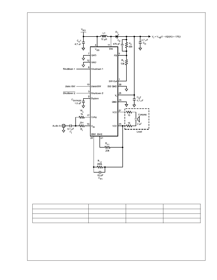
mono BTL operation the maximum power dissipation is 232mW.
JA
= 66∞C/W.
Note 4: Human body model, 100pF discharged through a 1.5k
resistor.
Note 5: Machine Model, 220pF≠240pF discharged through all pins.
Note 6: Typicals are measured at 25∞C and represent the parametric norm.
Note 7: Limits are guaranteed to National's AOQL (Average Outgoing Quality Level).
Note 8: Datasheet min/max specification limits are guaranteed by design, test, or statistical analysis.
Note 9: Shutdown current is measured in a normal room environment. The Shutdown pin should be driven as close as possible to GND for minimum shutdown
current.
Note 10: Noise measurements are dependent on the absolute values of closed loop gain setting resistors (input and feedback resistors).
LM4961
www.national.com
4