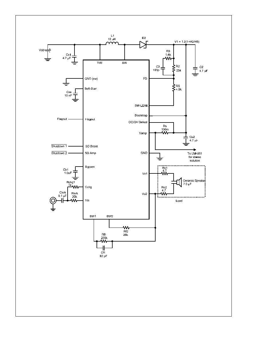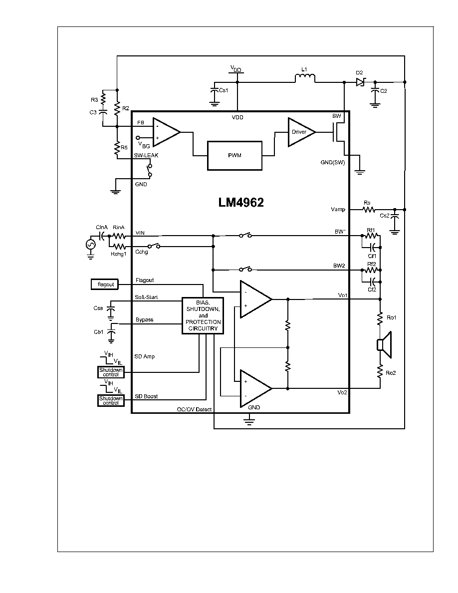
LM4962
Ceramic Speaker Driver
General Description
The LM4962 is an audio power amplifier primarily designed
for driving Ceramic Speaker for applications in Cell Phones,
Smart Phones, PDA's and other portable applications. It is
capable of driving 15Vpp (typ) BTL with less than 1%
THD+N from a 3.2V
DC
power supply. The LM4962 features
and low power consumption shutdown mode, an internal
thermal shutdown protection mechanism, along with over
current protection (OCP) and over voltage protection (OVP).
Boomer audio power amplifiers were designed specifically to
provide high quality output power with a minimal number of
external components. The LM4962 does not require boot-
strap capacitors, or snubber circuits.
The LM4962 also features a Band-Switch function which
allows the user to use one amplifier device for both receiver
(earpiece) mode and ringer/loudspeaker mode.
The LM4962 contains advanced pop & click circuitry that
eliminates noises which would otherwise occur during
turn-on and turn-off transitions. Additionally, the internal
boost converter features a soft-start function.
The LM4962 is unity-gain stable and can be configured by
external gain-setting resistors.
Key Specifications
n
Quiescent Power Supply Current (Boost Converter +
Amplifier)
9mA (typ)
n
Voltage Swing in BTL at 1% THD, f=1KHz
15Vp-p (typ)
n
Shutdown current
0.1µA (typ)
n
OVP
8.5V
<
V
AMP
<
9.5V
Features
n
Pop & click circuitry eliminates noise during turn-on and
turn-off transitions
n
Low current shutdown mode
n
Low quiescent current
n
Mono 15Vp-p BTL output, R
L
= 2µF+9.4
, f = 1kHz, 1%
THD+N
n
Over-current protection
n
Over-Voltage Protection
n
Unity-gain stable
n
External gain configuration capability
n
Including Band switch function
n
Leakage cut switch (SW-LEAK)
n
Soft-Start function
n
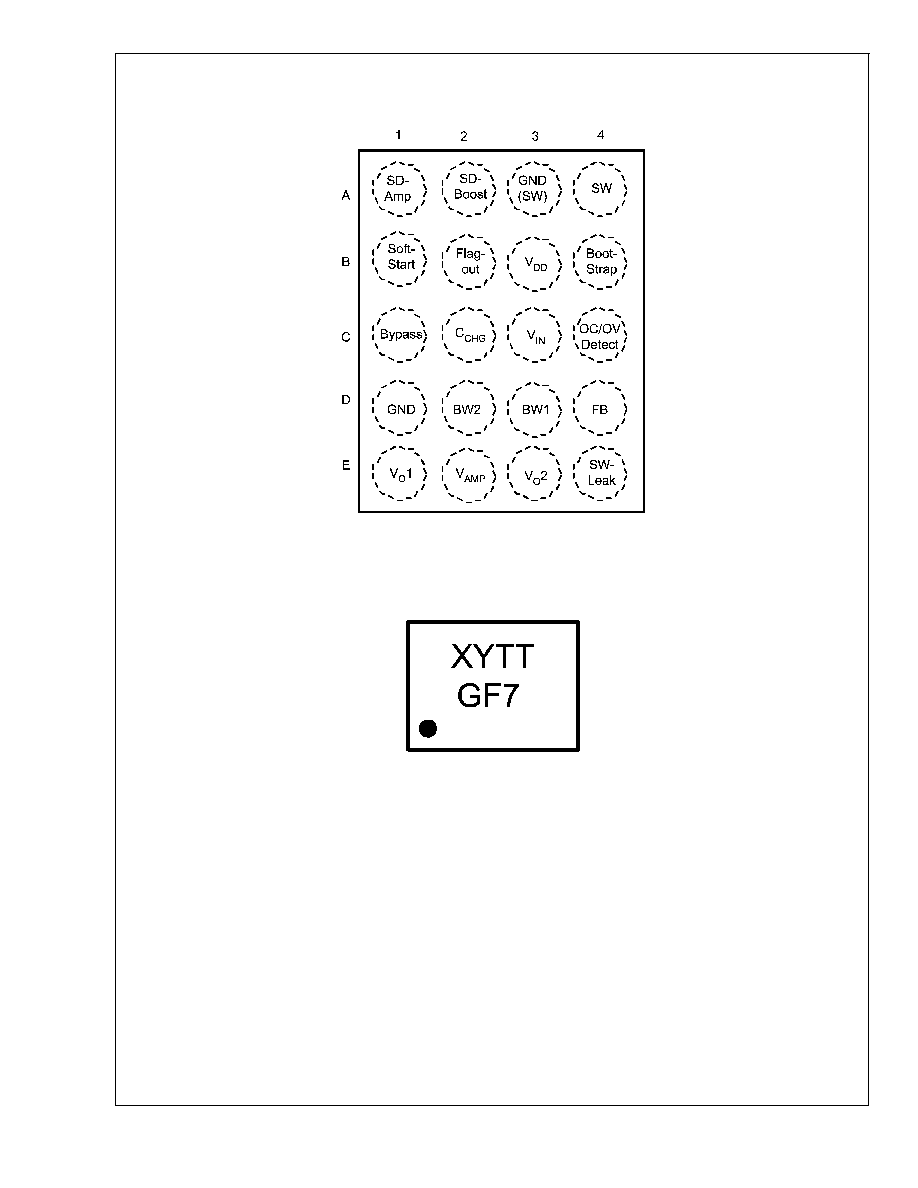
Space-saving micro SMD package (2mm x 2.5mm)
Applications
n
Smart phones
n
Mobile Phones and Multimedia Terminals
n
PDA's, Internet Appliances, and Portable Gaming
n
Portable DVD
n
Digital still cameras/camcorders
Boomer
Æ
is a registered trademark of National Semiconductor Corporation.
January 2006
LM4962
Ceramic
Speaker
Driver
© 2006 National Semiconductor Corporation
DS201422
www.national.com
Absolute Maximum Ratings
(Notes 1, 2)
If Military/Aerospace specified devices are required,
please contact the National Semiconductor Sales Office/
Distributors for availability and specifications.
Supply Voltage (V
DD
)
9.5V
Amplifier Supply Voltage (V
AMP
)
9.5V
Storage Temperature
-65∞C to +150∞C
Input Voltage
-0.3V to V
DD
+ 0.3V
Power Dissipation (Note 3)
Internally limited
ESD Susceptibility (Note 4)
2000V
ESD Susceptibility (Note 5)
200V
Junction Temperature
150∞C
Thermal Resistance
JA
(µSMD) (Note 12)
73∞C/W
See AN-1187 'Leadless Leadframe Packaging (LLP).'
Operating Ratings
Temperature Range
T
MIN
T
A
T
MAX
(Note 10)
-40∞C
T
A
+85∞C
Supply Voltage (V
DD
)
3.0V
<
V
DD
<
5.0V
Amplifier Supply Voltage (V
1
)
(Note 11)
2.7V
<
V
AMP
<
9.0V
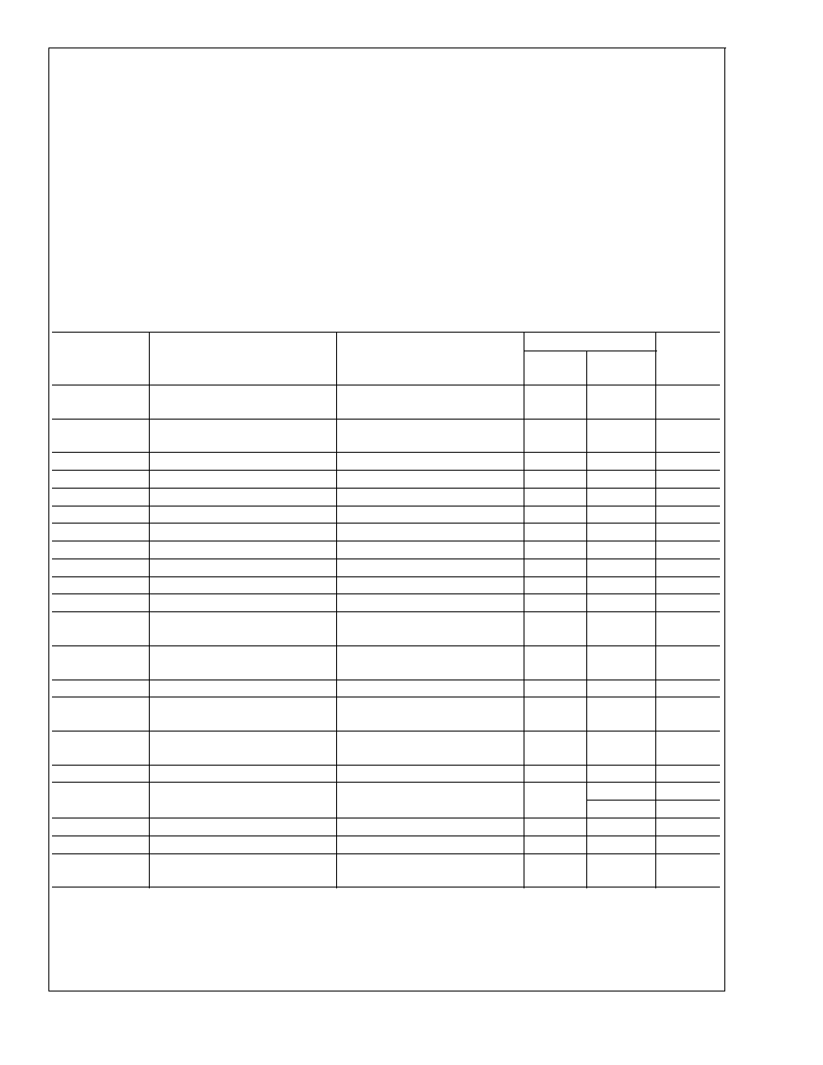
Electrical Characteristics
The following specifications apply for V
DD
= 3.2V, A
V-BTL
= 26dB, Z
L
= 2µF+9.4
, Cb = 1.0µF, R
2
=25K
, R
5
=4.9K
unless
otherwise specified. Limits apply for T
A
= 25∞C.
Symbol
Parameter
Conditions
LM4962
Units
(Limits)
Typical
(Note 6)
Limit
(Notes 7, 8)
I
DD
Quiescent Power Supply Current
in Boosted Ringer Mode
V
IN
= 0V,
9
12
mA (max)
Iddrcv
Quiescent Power Supply Current
in Receiver Mode
SD Boost = GND
SD Amp = V
DD
3
5
mA (max)
I
SD
Shutdown Current (Note 9)
SD Boost = SD Amp = GND
0.1
2.0
µA (max)
V
LH
Logic High Threshold Voltage
For SD Boost, SD Amp
1.2
V (min)
V
LL
Logic Low Threshold Voltage
For SD Boost, SD Amp
0.4
V (max)
R
PULLDOWN
Pulldown Resistor
For SD Amp, SD Boost
80
60
k
(min)
T
WUBC
Boost Converter Wake-up Time
C
SS
= 10nF
2
5
ms (max)
T
WUA
Audio Amplifier Wake-up Time
(For Vdd = 2.7V to 8.5V)
20
40
msec
V
OUT
Output Voltage Swing
THD = 1% (max), f = 1kHz
15
14
Vpp (min)
THD+N
Total Harmonic Distortion + Noise
Vout = 14Vpp, f = 1kHz
0.4
1.0
%
e
OS
Output Noise
A-Weighted Filter, V
IN
= 0V
125
µV
PSRR
Power Supply Rejection Ratio
V
RIPPLE
= 200mV
p-p
, f = 100Hz,
Input Referred
86
71
dB (min)
Ron-sw-leak
On Resistance on SW-Leak
SD Boost = GND
Isink = 100µA
30
50
(max)
Ron
Flagout On resistance
Isink = 1mA
50
100
(max)
Vovp
Sensitivity of Over Voltage
Protection on V
AMP
Flagout = GND
9.0
9.5
8.5
V (max)
V (min)
Vocp
Sensitivity of Over Current
Protection (Voltage Across R
S
)
Flagout = GND
185
275
75
mV (max)
mV (min)
Ileak
Leak Current on Flagout pin
Vflagout = V
DD
2
µA (max)
I
SW
SW Current Limit
2
2.7
A (max)
1.2
A (min)
TSD
Thermal Shutdown Temperature
150
∞C (min)
Vos
Output Offset Voltage
5
25
mV
V
FB
Feedback Voltage
SD Boost = V
DD
SD Amp = V
DD
1.23
1.15
1.31
V (min)
V (max)
LM4962
www.national.com
5