 | –≠–ª–µ–∫—Ç—Ä–æ–Ω–Ω—ã–π –∫–æ–º–ø–æ–Ω–µ–Ω—Ç: LM4981SQ | –°–∫–∞—á–∞—Ç—å:  PDF PDF  ZIP ZIP |
LM4981
Ground-Referenced, 80mW Stereo Headphone Amplifier
with Digital Volume Control
General Description
The
LM4981
is
a
stereo,
ground-referenced,
output
capacitor-less headphone amplifier capable of delivering
83mW of continuous average power into a 16
load with
less than 1% THD+N while operating from a single 3V
supply.
The LM4981 features a new circuit technology that utilizes a
charge pump to generate a negative reference voltage. This
allows the outputs to be biased about ground, thereby elimi-
nating output-coupling capacitors typically used with normal
single-ended loads.
The LM4981 provides high quality audio reproduction with
minimal external components. A ground referenced output
eliminates the output coupling capacitors typically required
to drive single-ended loads such as headphones. The
ground reference architecture reduces components count,
cost and board space consumption, making the LM4981
ideal for handheld MP3 players, mobile phones and other
portable equipment where board space is at a premium.
Eliminating the output capacitors also improves low fre-
quency response.
The LM4981 operates from a single 2.0V ≠ 4.2V supply, and
features a 2-wire, up/down volume control that sets the gain
of the amplifier between -33dB to +12dB in 16 discrete
steps. Selectable (active high/low) low power shutdown
mode provides flexible shutdown control. Superior click and
pop
suppression
eliminates
audible
transients
during
start-up and shutdown.
The LM4981 features an Automatic Standby Mode circuitry
(patent pending). In the absence of an input signal, after
approximately 12 seconds, the LM4981 goes into low cur-
rent standby mode. The LM4981 recovers into full power
operating mode immediately after a signal is applied to either
the left or right input pins. This feature saves power supply
current in battery operated applications.
Key Specifications
j
Improved PSRR at 217Hz
67dB (typ)
j
THD+N at 1kHz, 50mW
into 32
SE (3V)
1.0% (typ)
j
Single Supply Operation (V
DD
)
2.0 to 4.2V
j
Power Output at VDD = 3V,
RL = 16
, THD 1%
83mW (typ)
j
Shutdown Current
0.01µA (typ)
Features
n
Ground Referenced Outputs
n
No Output Coupling Capacitors
n
16-Step Volume Control
n
Auto-Standby Mode
n
High PSRR
n
Available in Space Saving LLP package
n
Low Power Shutdown Mode
n
Improved Click and Pop Suppression Eliminates Noises
During Turn-on and Turn-off Transients
n
2.0V to 4.2V Operation
n
83mW Per Channel Into 16
n
Selectable Shutdown Controls (Active High/Low)
Applications
n
Portable MP3 Players
n
Mobile Phones
n
PDAs
Boomer
Æ
is a registered trademark of National Semiconductor Corporation.
November 2005
LM4981
Ground-Referenced,
80mW
Stereo
Headphone
Amplifier
with
Digital
V
olume
Control
© 2005 National Semiconductor Corporation
DS201473
www.national.com
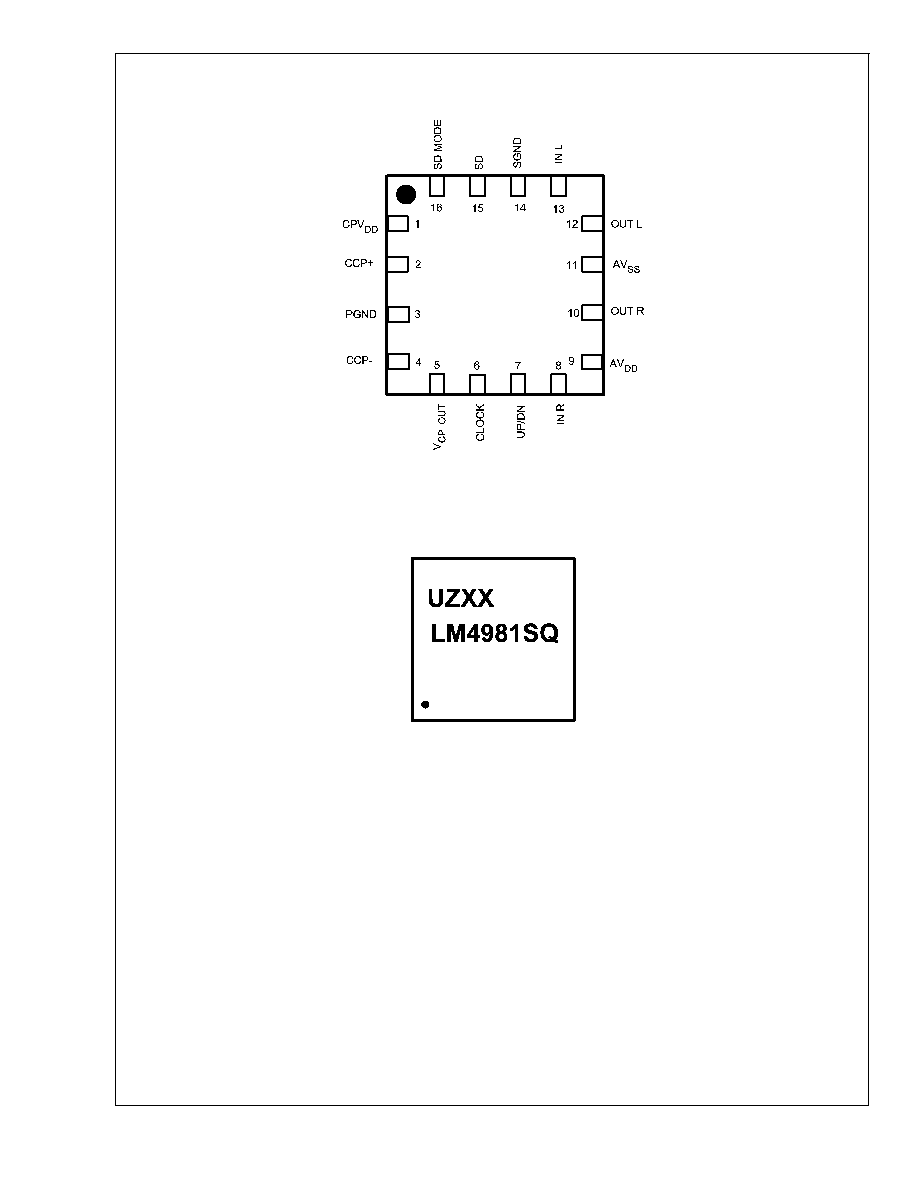
Connection Diagrams
LLP Package
20147338
Top View
Order Number LM4981SQ
See NS Package Number SQA16A
LLP Marking
20147321
Top View
U = Plant Code
ZX = Date Code
X = Die Traceability
Bottom Line = Part Number
LM4981
www.national.com
2
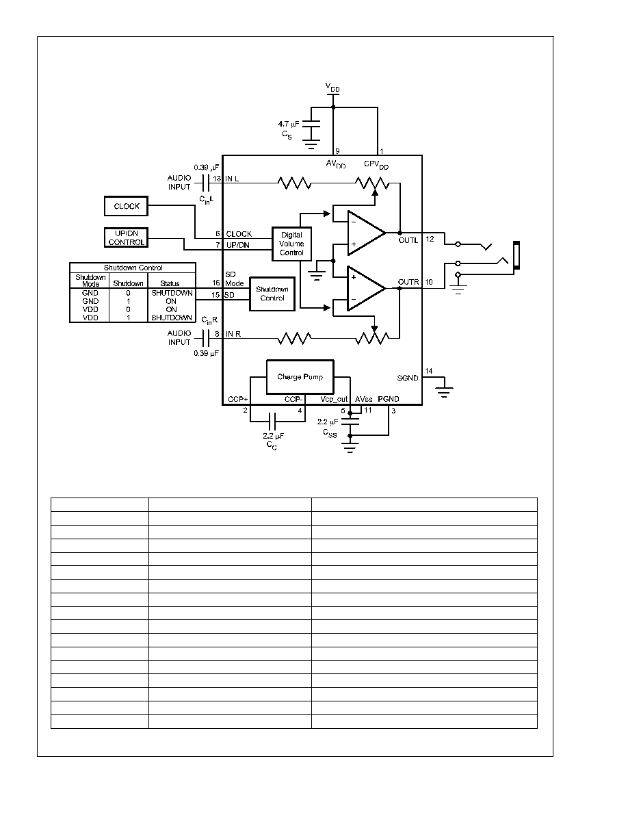
Typical Application
Pin
Name
Function
1
CP
VDD
Charge Pump Power Supply
2
CCP+
Positive Terminal- charge pump flying capacitor
3
PGND
Power Ground
4
CCP-
Negative Terminal- charge pump flying capacitor
5
VCP_OUT
Charge Pump Output
6
CLOCK
Clock
7
UP/DN
Up / Down
8
INR
Right Input
9
AV
DD
Positive Power Supply - Amplifier
10
OUT R
Right Output
11
AV
SS
Negative Power Supply - Amplifier
12
OUT L
Left Output
13
IN L
Left Input
14
SGND
Signal Ground
15
SD
Shutdown
16
SD MODE
Shutdown Mode Pin
20147337
FIGURE 1. Typical Audio Amplifier Application Circuit
LM4981
www.national.com
3
Absolute Maximum Ratings
(Note 2)
If Military/Aerospace specified devices are required,
please contact the National Semiconductor Sales Office/
Distributors for availability and specifications.
Supply Voltage
4.5V
Storage Temperature
-65∞C to +150∞C
Input Voltage
-0.3V to V
DD
+0.3V
Power Dissipation(Note 3)
Internally Limited
ESD Susceptibility (Note 4)
2500V
ESD Susceptibility (Note 5)
250V
Junction Temperature
150∞C
Operating Ratings
Temperature Range
T
MIN
T
A
T
MAX
-40∞C
T
A
85∞C
Supply Voltage (V
DD
)
2.0V
V
CC
4.2V
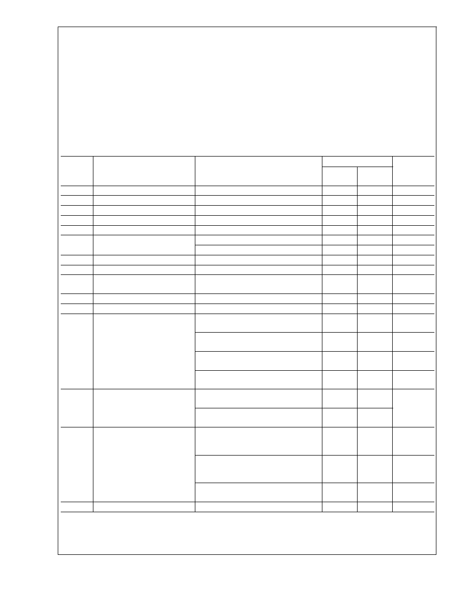
Electrical Characteristics V
DD
= 3V
(Notes 1, 2)
The following specifications apply for V
DD
= 3V, AV = 1V/V R
L
= 32
, f = 1kHz, unless otherwise specified. Limits apply to T
A
= 25∞C.
Symbol
Parameter
Conditions
LM4981
Units
(Limits)
Typical
(Note 6)
Limit
(Note 7)
I
DD
Quiescent Power Supply Current
V
IN
= 0V, R
L
=
7
10
mA
I
DD
Standby Power Supply Current
2.3
mA
I
SD
Shutdown Current
V
SD
= GND
0.1
3.5
µA
V
IH
Logic Input Voltage High
SHDN, SDM, CLOCK, U/D
0.7V
DD
V
V
IL
Logic Input Voltage Low
SHDN, SDM, CLOCK, U/D
0.3V
DD
V
Digital Volume
Input Referred Maximum Gain
12
dB
Input Referred Minimum Gain
≠33
dB
Volume Step Size
3
dB
Step Size Error
±
0.3
dB
Channel-to-Channel Volume
Tracking Error
All gain settings
0.15
dB
T
WU
Wake Up Time
300
µs
V
OS
Output Offset Voltage
R
L
= 32
1
5
mV
P
O
Output Power
THD+N = 1% (max); f = 1kHz,
R
L
= 16
, one channel
83
mW
THD+N = 1% (max); f = 1kHz,
R
L
= 32
, one channel
75
mW
THD+N = 1% (max); f = 1kHz,
R
L
= 16
, (two channels in phase)
40
33
mW (min)
THD+N = 1% (max); f = 1kHz,
R
L
= 32
, (two channels in phase)
47
43
mW (min)
THD+N
Total Harmonic Distortion
P
O
= 60mW, f = 1kHz, R
L
= 16
single channel
0.03
%
P
O
= 50mW, f = 1kHz, R
L
= 32
single channel
0.02
PSRR
Power Supply Rejection Ratio
V
RIPPLE
= 200mV
P-P
Sine,
f
RIPPLE
= 1kHz, Inputs AC GND,
Cl = 1µF
65
dB
V
RIPPLE
= 200mV
P-P
Sine,
f
RIPPLE
= 10kHz, Inputs AC GND,
Cl = 1µF
50
dB
V
RIPPLE
= 200mV
P-P
Sine,
f
RIPPLE
= 217Hz
67
dB
OS
Output Noise
A-Weighted Filter
11
µV
LM4981
www.national.com
4

Electrical Characteristics V
DD
= 3V
(Notes 1, 2) (Continued)
Note 1: All voltages are measured with respect to the GND pin unless other wise specified
Note 2: Absolute Maximum Ratings indicate limits beyond which damage to the device may occur. Operating Ratings indicate conditions for which the device is
functional but do not guarantee specific performance limits. Electrical Characteristics state DC and AC electrical specifications under particular test conditions which
guarantee specific performance limits. This assumes that the device is within the Operating Ratings. Specifications are not guaranteed for parameters where no limit
is given, however, the typical value is a good indication of device performance.
Note 3: The maximum power dissipation must be derated at elevated temperatures and is dictated by T
JMAX
,
JA
, and the ambient temperature, T
A
. The maximum
allowable power dissipation is P
DMAX
= (T
JMAX
≠ T
A
) /
JA
or the number given in Absolute Maximum Ratings, whichever is lower. For the LM4917, see power
derating currents for more information.
Note 4: Human body model, 100pF discharged through a 1.5k
resistor.
Note 5: Machine Model, 220pF-240pF discharged through all pins.
Note 6: Typical specifications are specified at +25∞C and represent parametric norm.
Note 7: Limits are guaranteed to National's AOQL (Average Outgoing Quality Level).
LM4981
www.national.com
5