LM4995
1.3 W Audio Power Amplifier
General Description
The LM4995 is an audio power amplifier primarily designed
for demanding applications in mobile phones and other por-
table communication device applications. It is capable of
delivering 1.2W of continuous average power to an 8
BTL
load with less than 1% distortion (THD+N) from a 5V
DC
power supply.
Boomer audio power amplifiers were designed specifically to
provide high quality output power with a minimal amount of
external components. The LM4995 does not require output
coupling capacitors or bootstrap capacitors, and therefore is
ideally suited for mobile phone and other low voltage appli-
cations where minimal power consumption is a primary re-
quirement.
The LM4995 features a low-power consumption shutdown
mode, which is achieved by driving the shutdown pin with
logic low. Additionally, the LM4995 features an internal ther-
mal shutdown protection mechanism.
The LM4995 contains advanced pop & click circuitry which
eliminates noise which would otherwise occur during turn-on
and turn-off transitions.
The LM4995 is unity-gain stable and can be configured by
external gain-setting resistors.
Key Specifications
j
PSRR at 3.6V (217Hz & 1kHz)
75dB
j
Output Power at 5.0V, 1% THD+N, 8
1.3W (typ)
j
Output Power at 3.6V, 1% THD+N, 8
625mW (typ)
j
Shutdown Current
0.01�A (typ)
Features
n
Available in space-saving 0.4mm pitch �SMD package
n
Ultra low current shutdown mode
n
BTL output can drive capacitive loads
n
Improved pop & click circuitry eliminates noise during
turn-on and turn-off transitions
n
2.4 - 5.5V operation
n
No output coupling capacitors, snubber networks or
bootstrap capacitors required
n
Unity-gain stable
n
External gain configuration capability
n
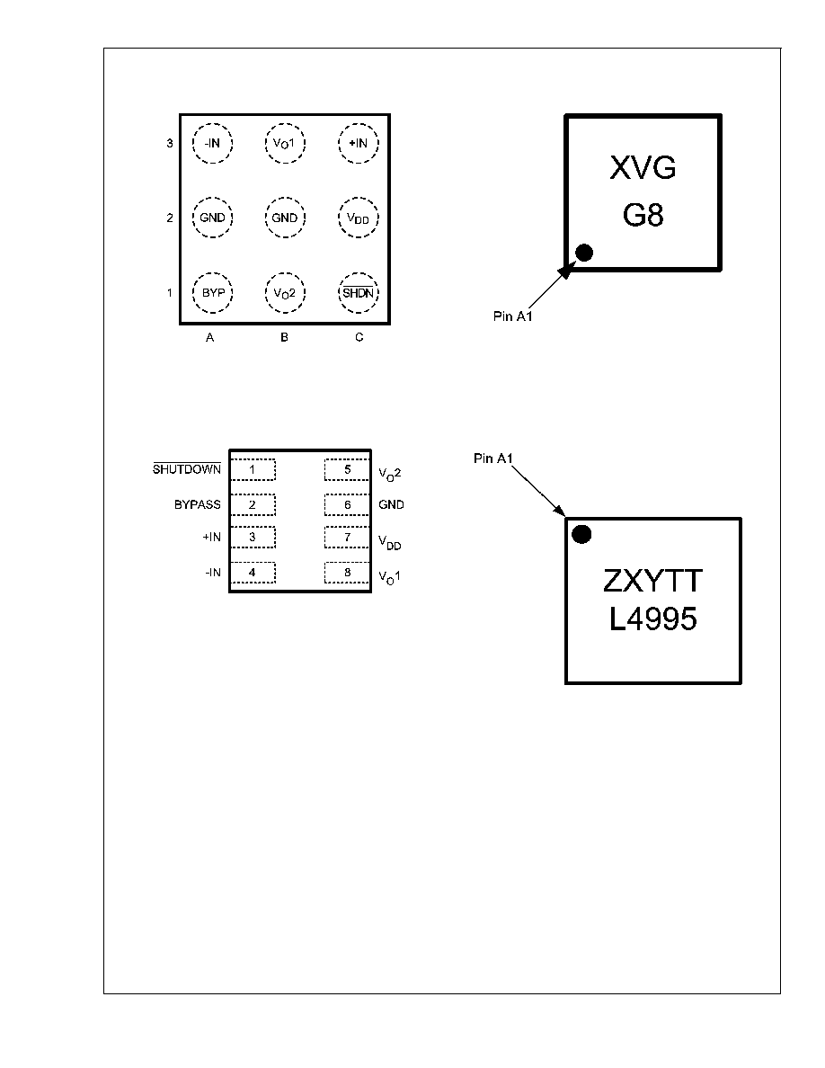
LLP package: 0.5mm pitch, 3 x 3 mm
Applications
n
Mobile Phones
n
PDAs
n
Portable electronic devices
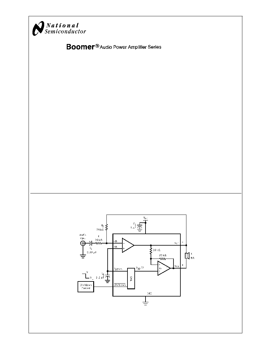
Typical Application
Boomer
�
is a registered trademark of National Semiconductor Corporation.
201599D3
FIGURE 1. Typical Audio Amplifier Application Circuit
August 2006
LM4995
1.3
W
Audio
Power
Amplifier
� 2006 National Semiconductor Corporation
DS201599
www.national.com
Absolute Maximum Ratings
(Note 2)
If Military/Aerospace specified devices are required,
please contact the National Semiconductor Sales Office/
Distributors for availability and specifications.
Supply Voltage (Note 10)
6.0V
Storage Temperature
-65�C to +150�C
Input Voltage
-0.3V to V
DD
+0.3V
Power Dissipation (Notes 3, 11)
Internally Limited
ESD Susceptibility (Note 4)
2000V
ESD Susceptibility (Note 5)
200V
Junction Temperature
150�C
Thermal Resistance
JA
(TM)
96.5�C/W
JA
(SD)
56�C/W
Operating Ratings
Temperature Range
T
MIN
T
A
T
MAX
-40�C
T
A
85�C
Supply Voltage
2.4V
V
DD
5.5V
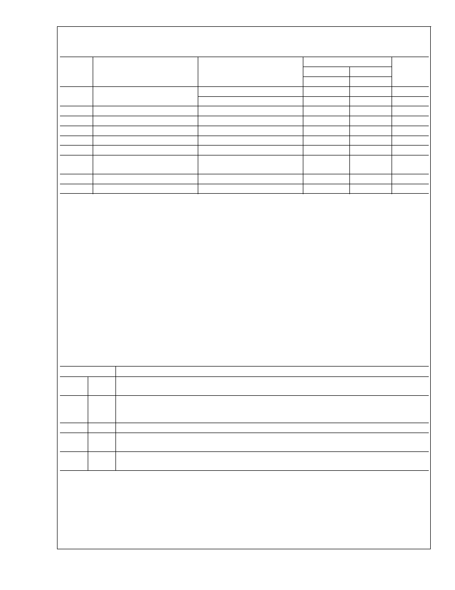
Electrical Characteristics V
DD
= 5V
(Notes 1, 2)
The following specifications apply for the circuit shown in Figure 1, unless otherwise specified. Limits apply for T
A
= 25�C.
Symbol
Parameter
Conditions
LM4995
Units
(Limits)
Typical
Limit
(Note 6)
(Notes 7, 8)
I
DD
Quiescent Power Supply Current
V
IN
= 0V, I
o
= 0A, No Load
1.5
2.5
mA (max)
V
IN
= 0V, I
o
= 0A, 8
Load
1.8
mA
I
SD
Shutdown Current
V
SD
= V
GND
0.01
1
�A (max)
V
OS
Output Offset Voltage
No Load
5
26
mV (max)
P
o
Output Power
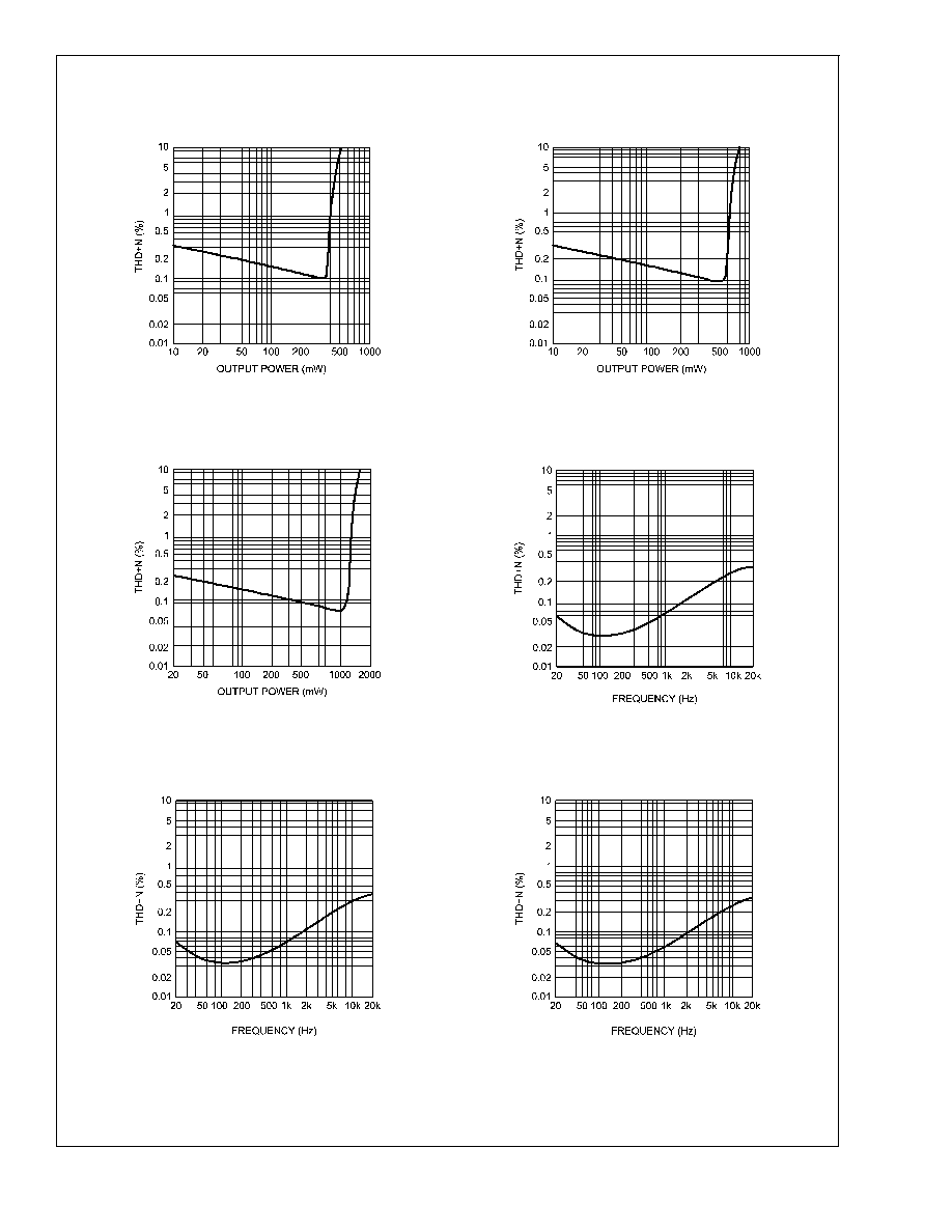
THD+N = 1% (max); f = 1 kHz
1.3 (TM)
1.25 (SD)
W
T
WU
Wake-up time
165
ms
THD+N
Total Harmonic Distortion + Noise
P
o
= 500mW
RMS
; f = 1kHz
0.08
%
PSRR
Power Supply Rejection Ratio
V
ripple
= 200mV sine p-p
Input terminated to GND
73 (f = 217Hz)
73 (f = 1kHz)
dB
V
SDIH
Shutdown Voltage Input High
1.5
V
V
SDIL
Shutdown Voltage Input Low
1.2
V
Electrical Characteristics V
DD
= 3.6V
(Notes 1, 2)
The following specifications apply for the circuit shown in Figure 1, unless otherwise specified. Limits apply for T
A
= 25�C.
Symbol
Parameter
Conditions
LM4995
Units
(Limits)
Typical
Limit
(Note 6)
(Notes 7, 8)
I
DD
Quiescent Power Supply Current
V
IN
= 0V, I
o
= 0A, No Load
1.3
2.3
mA (max)
V
IN
= 0V, I
o
= 0A, 8
Load
1.6
mA
I
SD
Shutdown Current
V
SD
= V
GND
0.01
1
�A (max)
V
OS
Output Offset Voltage
No Load
5
26
mV (max)
P
o
Output Power
THD+N = 1% (max); f = 1 kHz
625 (TM)
610 (SD)
mW
T
WU
Wake-up time
130
ms
THD+N
Total Harmonic Distortion + Noise
P
o
= 300mW
RMS
; f = 1kHz
0.07
%
PSRR
Power Supply Rejection Ratio
V
ripple
= 200mV sine p-p
Input terminated to GND
75 (f = 217Hz)
76 (f = 1kHz)
dB
V
SDIH
Shutdown Voltage Input High
1.3
V
V
SDIL
Shutdown Voltage Input Low
1
V
LM4995
www.national.com
3
Electrical Characteristics V
DD
= 3.0V
(Notes 1, 2)
The following specifications apply for the circuit shown in Figure 1, unless otherwise specified. Limits apply for T
A
= 25�C.
Symbol
Parameter
Conditions
LM4995
Units
(Limits)
Typical
Limit
(Note 6)
(Notes 7, 8)
I
DD
Quiescent Power Supply Current
V
IN
= 0V, I
o
= 0A, No Load
1.3
mA
V
IN
= 0V, I
o
= 0A, 8
Load
1.6
mA
I
SD
Shutdown Current
V
SD
= V
GND
0.01
�A
V
OS
Output Offset Voltage
No Load
5
mV
P
o
Output Power
THD+N = 1% (max); f = 1 kHz
400
mW
T
WU
Wake-up time
110
ms
THD+N
Total Harmonic Distortion + Noise
P
o
= 250mW
RMS
; f = 1kHz
0.07
%
PSRR
Power Supply Rejection Ratio
V
ripple
= 200mV sine p-p
Input terminated to GND
74 (f = 217Hz)
75 (f = 1kHz)
dB
V
SDIH
Shutdown Voltage Input High
1.2
V
V
SDIL
Shutdown Voltage Input Low
1
V
Note 1: All voltages are measured with respect to the ground pin, unless otherwise specified.
Note 2: Absolute Maximum Ratings indicate limits beyond which damage to the device may occur. Operating Ratings indicate conditions for which the device is
functional, but do not guarantee specific performance limits. Electrical Characteristics state DC and AC electrical specifications under particular test conditions which
guarantee specific performance limits. This assumes that the device is within the Operating Ratings. Specifications are not guaranteed for parameters where no limit
is given, however, the typical value is a good indication of device performance.
Note 3: The maximum power dissipation must be derated at elevated temperatures and is dictated by T
JMAX
,
JA
, and the ambient temperature T
A
. The maximum
allowable power dissipation is P
DMAX
= (T
JMAX
�T
A
)/
JA
or the number given in Absolute Maximum Ratings, whichever is lower. For the LM4995, see power derating
curves for additional information.
Note 4: Human body model, 100pF discharged through a 1.5k
resistor.
Note 5: Machine Model, 220pF�240pF discharged through all pins.
Note 6: Typicals are measured at 25�C and represent the parametric norm.
Note 7: Limits are guaranteed to National's AOQL (Average Outgoing Quality Level).
Note 8: Datasheet min/max specification limits are guaranteed by design, test, or statistical analysis.
Note 9: R
OUT
is measured from the output pin to ground. This value represents the parallel combination of the 10k
output resistors and the two 20k resistors.
Note 10: If the product is in Shutdown mode and V
DD
exceeds 6V (to a max of 8V V
DD
), then most of the excess current will flow through the ESD protection circuits.
If the source impedance limits the current to a max of 10mA, then the device will be protected. If the device is enabled when V
DD
is greater than 5.5V and less than
6.5V, no damage will occur, although operation life will be reduced. Operation above 6.5V with no current limit will result in permanent damage.
Note 11: Maximum power dissipation in the device (P
DMAX
) occurs at an output power level significantly below full output power. P
DMAX
can be calculated using
Equation 1 shown in the Application Information section. It may also be obtained from the power dissipation graphs.
External Components Description
(Figure 1)
Components
Functional Description
1.
R
i
Inverting input resistance which sets the closed-loop gain in conjunction with R
f
. This resistor also forms a
high pass filter with C
i
at f
C
= 1/(2
R
i
C
i
).
2.
C
i
Input coupling capacitor which blocks the DC voltage at the amplifiers input terminals. Also creates a
highpass filter with R
i
at f
C
= 1/(2
R
i
C
i
). Refer to the section, Proper Selection of External Components,
for an explanation of how to determine the value of C
i
.
3.
R
f
Feedback resistance which sets the closed-loop gain in conjunction with R
i
.
4.
C
S
Supply bypass capacitor which provides power supply filtering. Refer to the Power Supply Bypassing
section for information concerning proper placement and selection of the supply bypass capacitor.
5.
C
B
Bypass pin capacitor which provides half-supply filtering. Refer to the section, Proper Selection of External
Components, for information concerning proper placement and selection of C
B
.
LM4995
www.national.com
4