 | –≠–ª–µ–∫—Ç—Ä–æ–Ω–Ω—ã–π –∫–æ–º–ø–æ–Ω–µ–Ω—Ç: LM5008 | –°–∫–∞—á–∞—Ç—å:  PDF PDF  ZIP ZIP |
LM5008
High Voltage (100V) Step Down Switching Regulator
General Description
The LM5008 Step Down Switching Regulator features all of
the functions needed to implement a low cost, efficient, Buck
bias regulator. This high voltage regulator contains an 100 V
N-Channel Buck Switch. The device is easy to implement
and is provided in the MSOP-8 and the thermally enhanced
LLP-8 packages. The regulator is based on a hysteretic
control scheme using an ON time inversely proportional to
V
IN
. This feature allows the operating frequency to remain
relatively constant. The hysteretic control requires no loop
compensation. An intelligent current limit is implemented
with forced OFF time, which is inversely proportional to Vout.
This scheme ensures short circuit protection while providing
minimum foldback. Other protection features include: Ther-
mal Shutdown, V
CC
under-voltage lockout, Gate drive under-
voltage lockout, and Max Duty Cycle limiter
Features
n
Integrated 100V, N-Channel buck switch
n
Internal V
CC
regulator
n
No loop compensation required
n
Ultra-Fast transient response
n
On time varies inversely with line voltage
n
Operating frequency remains constant with varying line
voltage and load current
n
Adjustable output voltage
n
Highly efficient operation
n
Precision internal reference
n
Low bias current
n
Intelligent current limit protection
n
Thermal shutdown
Typical Applications
n
Non-Isolated Telecommunication Buck Regulator
n
Secondary High Voltage Post Regulator
n
+42V Automotive Systems
Package
n
MSOP - 8
n
LLP - 8 (4mm x 4mm)
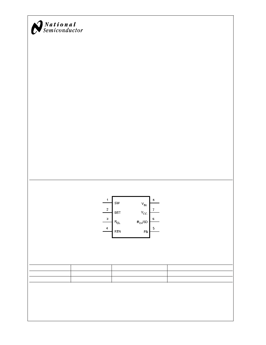
Connection Diagram
20097902
8-Lead MSOP, LLP
Ordering Information
Order Number
Package Type
NSC Package Drawing
Supplied As
LM5008MM
MSOP-8
MUA08A
1000 Units on Tape and Reel
LM5008SD
LLP-8
SDC08A
1000 Units on Tape and Reel
October 2004
LM5008
High
V
oltage
(100V)
Step
Down
Switching
Regulator
© 2004 National Semiconductor Corporation
DS200979
www.national.com
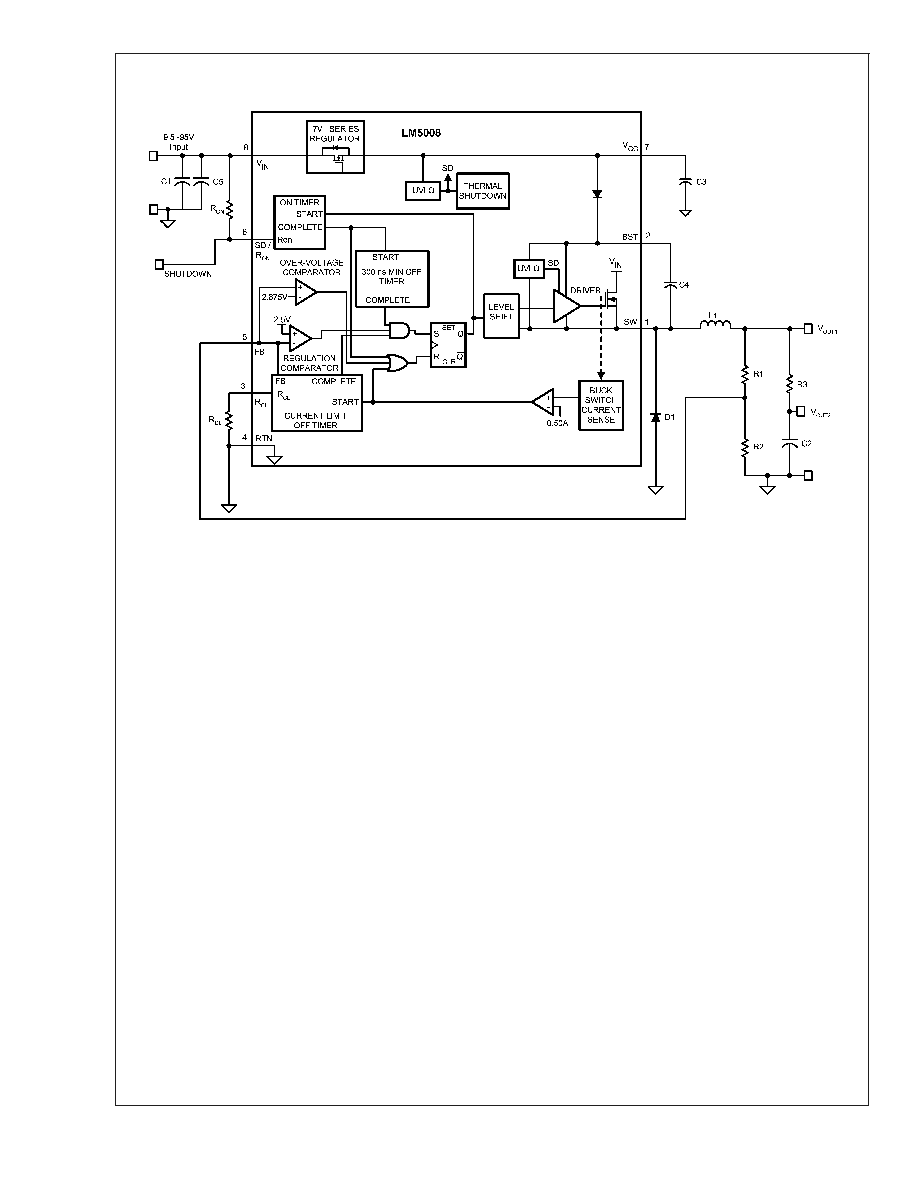
Typical Application Circuit and Block Diagram
20097901
FIGURE 1.
LM5008
www.national.com
2
Pin Description
PIN
NAME
DESCRIPTION
APPLICATION INFORMATION
1
SW
Switching Node
Power switching node. Connect to the output
inductor, re-circulating diode, and bootstrap
capacitor.
2
BST
Boost Pin (Boot≠strap capacitor input)
An external capacitor is required between the BST
and the SW pins. A 0.01µF ceramic capacitor is
recommended. An internal diode charges the
capacitor from V
CC
.
3
R
CL
Current Limit OFF time set pin
Toff = 10
-5
/ (0.285 + (FB / 6.35 x 10
- 6
x R
CL
))
A resistor between this pin and RTN sets the
off-time when current limit is detected. The off-time
is preset to 35µs if FB = 0V.
4
RTN
Ground pin
Ground for the entire circuit.
5
FB
Feedback input from Regulated Output
This pin is connected to the inverting input of the
internal regulation comparator. The regulation
threshold is 2.5V.
6
R
ON
/SD
On time set pin
Ton = 1.25 x 10
-10
R
ON
/ V
IN
A resistor between this pin and V
IN
sets the switch
on time as a function of V
IN
. The minimum
recommended on time is 400ns at the maximum
input voltage. This pin can be used for remote
shutdown.
7
V
CC
Output from the internal high voltage series pass
regulator. Regulated at 7.0V.
If an auxiliary voltage is available to raise the
voltage on this pin, above the regulation setpoint
(7V), the internal series pass regulator will
shutdown, reducing the IC power dissipation. Do not
exceed 14V. This voltage provides gate drive power
for the internal Buck switch. An internal diode is
provided between this pin and the BST pin. A local
0.1µF decoupling capacitor is recommended. Series
pass regulator is current limited to 10mA.
8
V
IN
Input voltage
Recommended operating range: 9.5V to 95V.
LM5008
www.national.com
3
Absolute Maximum Ratings
(Note 1)
If Military/Aerospace specified devices are required,
please contact the National Semiconductor Sales Office/
Distributors for availability and specifications.
V
IN
to GND
-0.3V to 100V
BST to GND
-0.3V to 114V
SW to GND (Steady State)
-1V
ESD Rating (Note 5)
Human Body Model
1.5kV
BST to V
CC
100V
BST to SW
14V
V
CC
to GND
14V
All Other Inputs to GND
-0.3 to 7V
Lead Temperature (Soldering 4 sec)
200∞C
Storage Temperature Range
-55∞C to +150∞C
Operating Ratings
(Note 1)
V
IN
9.5V to 95V
Operating Junction Temperature
-40∞C to + 125∞C
Electrical Characteristics
Specifications with standard typeface are for T
J
= 25∞C, and those with boldface type apply over full Operating Junction
Temperature range. V
IN
= 48V, unless otherwise stated (Note 3).
Symbol
Parameter
Conditions
Min
Typ
Max
Units
V
CC
Supply
V
CC
Reg
V
CC
Regulator Output
6.6
7
7.4
V
V
CC
Current Limit
(Note 4)
9.5
mA
V
CC
undervoltage Lockout
Voltage (V
CC
increasing)
6.3
V
V
CC
Undervoltage Hysteresis
200
mV
V
CC
UVLO Delay (filter)
100mV overdrive
10
µs
I
IN
Operating Current
Non-Switching, FB = 3V
485
675
µA
I
IN
Shutdown Current
R
ON
/SD = 0V
76
150
µA
Switch Characteristics
Buck Switch Rds(on)
I
TEST
= 200mA, (Note 6)
1.15
2.47
Gate Drive UVLO
V
BST
- V
SW
Rising
3.4
4.5
5.5
V
Gate Drive UVLO Hysteresis
430
mV
Current Limit
Current Limit Threshold
0.41
0.51
0.61
A
Current Limit Response Time
I
switch
Overdrive = 0.1A
Time to Switch Off
400
ns
OFF time generator (test 1)
FB=0V, R
CL
= 100K
35
µs
OFF time generator (test 2)
FB=2.3V, R
CL
= 100K
2.56
µs
On Time Generator
T
ON
- 1
Vin = 10V
Ron = 200K
2.15
2.77
3.5
µs
T
ON
- 2
Vin = 95V
Ron = 200K
200
300
420
ns
Remote Shutdown Threshold
Rising
0.40
0.70
1.05
V
Remote Shutdown Hysteresis
35
mV
LM5008
www.national.com
4

Electrical Characteristics
(Continued)
Specifications with standard typeface are for T
J
= 25∞C, and those with boldface type apply over full Operating Junction
Temperature range. V
IN
= 48V, unless otherwise stated (Note 3).
Symbol
Parameter
Conditions
Min
Typ
Max
Units
Minimum Off Time
Minimum Off Timer
FB = 0V
300
ns
Regulation and OV Comparators
FB Reference Threshold
Internal reference
Trip point for switch ON
2.445
2.5
2.550
V
FB Over-Voltage Threshold
Trip point for switch OFF
2.875
V
FB Bias Current
100
nA
Thermal Shutdown
Tsd
Thermal Shutdown Temp.
165
∞C
Thermal Shutdown Hysteresis
25
∞C
Thermal Resistance
JA
Junction to Ambient
MUA Package
200
∞C/W
SDC Package
40
∞C/W
Note 1: Absolute Maximum Ratings are limits beyond which damage to the device may occur. Operating Ratings are conditions under which operation of the device
is intended to be functional. For guaranteed specifications and test conditions, see the Electrical Characteristics.
Note 2: For detailed information on soldering plastic MSOP and LLP packages, refer to the Packaging Data Book available from National Semiconductor
Corporation.
Note 3: All limits are guaranteed. All electrical characteristics having room temperature limits are tested during production with T
A
= T
J
= 25∞C. All hot and cold limits
are guaranteed by correlating the electrical characteristics to process and temperature variations and applying statistical process control.
Note 4: The V
CC
output is intended as a self bias for the internal gate drive power and control circuits. Device thermal limitations limit external loading.
Note 5: The human body model is a 100pF capacitor discharged through a 1.5k
resistor into each pin.
Note 6: For devices procured in the LLP-8 package the Rds(on) limits are guaranteed by design characterization data only.
LM5008
www.national.com
5
Typical Performance Characteristics
20097909
FIGURE 2. I
CC
Current vs Applied V
CC
Voltage
20097910
FIGURE 3. ON-Time vs Input Voltage and R
ON
20097911
FIGURE 4. Maximum Frequency vs V
OUT
and V
IN
20097912
FIGURE 5. Current Limit Off-Time vs V
FB
and R
CL
LM5008
www.national.com
6
Typical Performance
Characteristics
(Continued)
Functional Description
The LM5008 Step Down Switching Regulator features all the
functions needed to implement a low cost, efficient, Buck
bias power converter. This high voltage regulator contains a
100 V N-Channel Buck Switch, is easy to implement and is
provided in the MSOP-8 and the thermally enhanced LLP-8
packages. The regulator is based on a hysteretic control
scheme using an on-time inversely proportional to V
IN
. The
hysteretic control requires no loop compensation. Current
limit is implemented with forced off-time, which is inversely
proportional to V
OUT
. This scheme ensures short circuit pro-
tection while providing minimum foldback. The Functional
Block Diagram of the LM5008 is shown in Figure 1.
The LM5008 can be applied in numerous applications to
efficiently regulate down higher voltages. This regulator is
well suited for 48 Volt Telecom and the new 42V Automotive
power bus ranges. Protection features include: Thermal
Shutdown, V
CC
under-voltage lockout, Gate drive under-
voltage lockout, Max Duty Cycle limit timer and the intelligent
current limit off timer.
Hysteretic Control Circuit
Overview
The LM5008 is a Buck DC-DC regulator that uses a control
scheme in which the on-time varies inversely with line volt-
age (V
IN
). Control is based on a comparator and the on-time
one-shot, with the output voltage feedback (FB) compared to
an internal reference (2.5V). If the FB level is below the
reference the buck switch is turned on for a fixed time
determined by the line voltage and a programming resistor
(R
ON
). Following the ON period the switch will remain off for
at least the minimum off-timer period of 300ns. If FB is still
below the reference at that time the switch will turn on again
for another on-time period. This will continue until regulation
is achieved.
The LM5008 operates in discontinuous conduction mode at
light load currents, and continuous conduction mode at
heavy load current. In discontinuous conduction mode, cur-
rent through the output inductor starts at zero and ramps up
to a peak during the on-time, then ramps back to zero before
20097923
FIGURE 6. Efficiency vs V
IN
(Circuit of Figure 13)
20097927
FIGURE 7. Efficiency vs Load Current vs V
IN
(Circuit of Figure 13)
20097924
FIGURE 8. Output Voltage vs Load Current
(Circuit of Figure 13)
LM5008
www.national.com
7
Hysteretic Control Circuit
Overview
(Continued)
the end of the off-time. The next on-time period starts when
the voltage at FB falls below the internal reference - until
then the inductor current remains zero. In this mode the
operating frequency is lower than in continuous conduction
mode, and varies with load current. Therefore at light loads
the conversion efficiency is maintained, since the switching
losses reduce with the reduction in load and frequency. The
discontinuous operating frequency can be calculated as fol-
lows:
where R
L
= the load resistance
In continuous conduction mode, current flows continuously
through the inductor and never ramps down to zero. In this
mode the operating frequency is greater than the discontinu-
ous mode frequency and remains relatively constant with
load and line variations. The approximate continuous mode
operating frequency can be calculated as follows:
(1)
The output voltage (V
OUT
) can be programmed by two ex-
ternal resistors as shown in Figure 1. The regulation point
can be calculated as follows:
V
OUT
= 2.5 x (R1 + R2) / R2
All hysteretic regulators regulate the output voltage based on
ripple voltage at the feedback input, requiring a minimum
amount of ESR for the output capacitor C2. A minimum of
25mV to 50mV of ripple voltage at the feedback pin (FB) is
required for the LM5008. In cases where the capacitor ESR
is too small, additional series resistance may be required
(R3 in Figure 1).
For applications where lower output voltage ripple is re-
quired the output can be taken directly from a low ESR
output capacitor, as shown in Figure 9. However, R3 slightly
degrades the load regulation.
High Voltage Start-up Regulator
The LM5008 contains an internal high voltage startup regu-
lator. The input pin (V
IN
) can be connected directly to the line
voltages up to 95 Volts, with transient capability to 100 volts.
The regulator is internally current limited to 9.5mA at V
CC
.
Upon power up, the regulator sources current into the exter-
nal capacitor at V
CC
(C3). When the voltage on the V
CC
pin
reaches the under-voltage lockout threshold of 6.3V, the
buck switch is enabled.
In applications involving a high value for V
IN
, where power
dissipation in the V
CC
regulator is a concern, an auxiliary
voltage can be diode connected to the V
CC
pin. Setting the
auxiliary voltage to 8.0 -14V will shut off the internal regula-
tor, reducing internal power dissipation. See Figure 10. The
current required into the V
CC
pin is shown in Figure 2.
20097905
FIGURE 9. Low Ripple Output Configuration
LM5008
www.national.com
8

High Voltage Start-up Regulator
(Continued)
Regulation Comparator
The feedback voltage at FB is compared to an internal 2.5V
reference. In normal operation (the output voltage is regu-
lated), an on-time period is initiated when the voltage at FB
falls below 2.5V. The buck switch will stay on for the on-time,
causing the FB voltage to rise above 2.5V. After the on-time
period, the buck switch will stay off until the FB voltage again
falls below 2.5V. During start-up, the FB voltage will be below
2.5V at the end of each on-time, resulting in the minimum
off-time of 300 ns. Bias current at the FB pin is nominally 100
nA.
Over-Voltage Comparator
The feedback voltage at FB is compared to an internal
2.875V reference. If the voltage at FB rises above 2.875V
the on-time pulse is immediately terminated. This condition
can occur if the input voltage, or the output load, change
suddenly. The buck switch will not turn on again until the
voltage at FB falls below 2.5V.
ON-Time Generator and Shutdown
The on-time for the LM5008 is determined by the R
ON
resis-
tor, and is inversely proportional to the input voltage (Vin),
resulting in a nearly constant frequency as Vin is varied over
its range. The on-time equation for the LM5008 is:
T
ON
= 1.25 x 10
-10
x R
ON
/ V
IN
(2)
See Figure 3. R
ON
should be selected for a minimum on-time
(at maximum V
IN
) greater than 400 ns, for proper current
limit operation. This requirement limits the maximum fre-
quency for each application, depending on V
IN
and V
OUT
.
See Figure 4.
The LM5008 can be remotely disabled by taking the R
ON
/SD
pin to ground. See Figure 11. The voltage at the R
ON
/SD pin
is between 1.5 and 3.0 volts, depending on Vin and the value
of the R
ON
resistor.
20097906
FIGURE 10. Self Biased Configuration
20097907
FIGURE 11. Shutdown Implementation
LM5008
www.national.com
9
Current Limit
The LM5008 contains an intelligent current limit OFF timer. If
the current in the Buck switch exceeds 0.5A the present
cycle is immediately terminated, and a non-resetable OFF
timer is initiated. The length of off-time is controlled by an
external resistor (R
CL
) and the FB voltage (see Figure 5).
When FB = 0V, a maximum off-time is required, and the time
is preset to 35µs. This condition occurs when the output is
shorted, and during the initial part of start-up. This amount of
time ensures safe short circuit operation up to the maximum
input voltage of 95V. In cases of overload where the FB
voltage is above zero volts (not a short circuit) the current
limit off-time will be less than 35µs. Reducing the off-time
during less severe overloads reduces the amount of fold-
back, recovery time, and the start-up time. The off-time is
calculated from the following equation:
T
OFF
= 10
-5
/ (0.285 + (V
FB
/ 6.35 x 10
-6
x R
CL
))
(3)
The current limit sensing circuit is blanked for the first 50-
70ns of each on-time so it is not falsely tripped by the current
surge which occurs at turn-on. The current surge is required
by the re-circulating diode (D1) for its turn-off recovery.
N - Channel Buck Switch and
Driver
The LM5008 integrates an N-Channel Buck switch and as-
sociated floating high voltage gate driver. The gate driver
circuit works in conjunction with an external bootstrap ca-
pacitor and an internal high voltage diode. A 0.01µF ceramic
capacitor (C4) connected between the BST pin and SW pin
provides the voltage to the driver during the on-time.
During each off-time, the SW pin is at approximately 0V, and
the bootstrap capacitor charges from Vcc through the inter-
nal diode. The minimum OFF timer, set to 300ns, ensures a
minimum time each cycle to recharge the bootstrap capaci-
tor.
An external re-circulating diode (D1) carries the inductor
current after the internal Buck switch turns off. This diode
must be of the Ultra-fast or Schottky type to minimize turn-on
losses and current over-shoot.
Thermal Protection
The LM5008 should be operated so the junction temperature
does not exceed 125∞C during normal operation. An internal
Thermal Shutdown circuit is provided to protect the LM5008
in the event of a higher than normal junction temperature.
When activated, typically at 165∞C, the controller is forced
into a low power reset state, disabling the buck switch and
the V
CC
regulator. This feature prevents catastrophic failures
from accidental device overheating. When the junction tem-
perature reduces below 140∞C (typical hysteresis = 25∞C),
the Vcc regulator is enabled, and normal operation is re-
sumed.
Applications Information
SELECTION OF EXTERNAL COMPONENTS
A guide for determining the component values will be illus-
trated with a design example. Refer to Figure 1. The follow-
ing steps will configure the LM5008 for:
∑
Input voltage range (Vin): 12V to 95V
∑
Output voltage (V
OUT1
): 10V
∑
Load current (for continuous conduction mode): 100 mA
to 300 mA
∑
Maximum ripple at V
OUT2
: 100 mVp-p at maximum input
voltage
R1 and R2: From Figure 1, V
OUT1
= V
FB
x (R1 + R2) / R2,
and since V
FB
= 2.5V, the ratio of R1 to R2 calculates as 3:1.
Standard values of 3.01 k
(R1) and 1.00 k (R2) are
chosen. Other values could be used as long as the 3:1 ratio
is maintained. The selected values, however, provide a small
amount of output loading (2.5 mA) in the event the main load
is disconnected. This allows the circuit to maintain regulation
until the main load is reconnected.
F
s
and R
ON
: The recommended operating frequency range
for the LM5008 is 50kHz to 600 kHz. Unless the application
requires a specific frequency, the choice of frequency is
generally a compromise since it affects the size of L1 and
C2, and the switching losses. The maximum allowed fre-
quency, based on a minimum on-time of 400 ns, is calcu-
lated from:
F
MAX
= V
OUT
/ V
INMAX
x 400ns
For this exercise, Fmax = 263kHz. From equation 1, R
ON
calculates to 304 k
. A standard value 357 k resistor will
be used to allow for tolerances in equation 1, resulting in a
frequency of 224kHz.
L1: The main parameter affected by the inductor is the
output current ripple amplitude. The choice of inductor value
therefore depends on both the minimum and maximum load
currents, keeping in mind that the maximum ripple current
occurs at maximum Vin.
a) Minimum load current: To maintain continuous conduc-
tion at minimum Io (100 mA), the ripple amplitude (I
OR
) must
be less than 200 mA p-p so the lower peak of the waveform
does not reach zero. L1 is calculated using the following
equation:
At Vin = 95V, L1(min) calculates to 200 µH. The next larger
standard value (220 µH) is chosen and with this value I
OR
calculates to 181 mA p-p at Vin = 95V, and 34 mA p-p at Vin
= 12V.
b) Maximum load current: At a load current of 300 mA, the
peak of the ripple waveform must not reach the minimum
guaranteed value of the LM5008's current limit threshold
(410 mA). Therefore the ripple amplitude must be less than
220 mA p-p, which is already satisfied in the above calcula-
tion. With L1 = 220 µH, at maximum Vin and Io, the peak of
the ripple will be 391 mA. While L1 must carry this peak
current without saturating or exceeding its temperature rat-
ing, it also must be capable of carrying the maximum guar-
anteed value of the LM5008's current limit threshold (610
mA) without saturating, since the current limit is reached
during startup.
The DC resistance of the inductor should be as low as
possible. For example, if the inductor's DCR is one ohm, the
power dissipated at maximum load current is 0.09W. While
small, it is not insignificant compared to the load power of
3W.
C3: The capacitor on the V
CC
output provides not only noise
filtering and stability, but its primary purpose is to prevent
LM5008
www.national.com
10
Applications Information
(Continued)
false triggering of the V
CC
UVLO at the buck switch on/off
transitions. For this reason, C3 should be no smaller than 0.1
µF.
C2, and R3: When selecting the output filter capacitor C2,
the items to consider are ripple voltage due to its ESR, ripple
voltage due to its capacitance, and the nature of the load.
a) ESR and R3: A low ESR for C2 is generally desirable so
as to minimize power losses and heating within the capaci-
tor. However, a hysteretic regulator requires a minimum
amount of ripple voltage at the feedback input for proper loop
operation. For the LM5008 the minimum ripple required at
pin 5 is 25 mV p-p, requiring a minimum ripple at V
OUT1
of
100 mV. Since the minimum ripple current (at minimum Vin)
is 34 mA p-p, the minimum ESR required at V
OUT1
is 100mV/
34mA = 2.94
. Since quality capacitors for SMPS applica-
tions have an ESR considerably less than this, R3 is inserted
as shown in Figure 1. R3's value, along with C2's ESR, must
result in at least 25 mV p-p ripple at pin 5. Generally, R3 will
be 0.5 to 3.0
.
b) Nature of the Load: The load can be connected to V
OUT1
or V
OUT2
. V
OUT1
provides good regulation, but with a ripple
voltage which ranges from 100 mV (
@
Vin = 12V) to 500mV
(
@
Vin = 95V). Alternatively, V
OUT2
provides low ripple, but
lower regulation due to R3.
For a maximum allowed ripple voltage of 100 mVp-p at
V
OUT2
(
@
Vin = 95V), assume an ESR of 0.4
for C2. At
maximum Vin, the ripple current is 181 mAp-p, creating a
ripple voltage of 72 mVp-p. This leaves 28 mVp-p of ripple
due to the capacitance. The average current into C2 due to
the ripple current is calculated using the waveform in Figure
12.
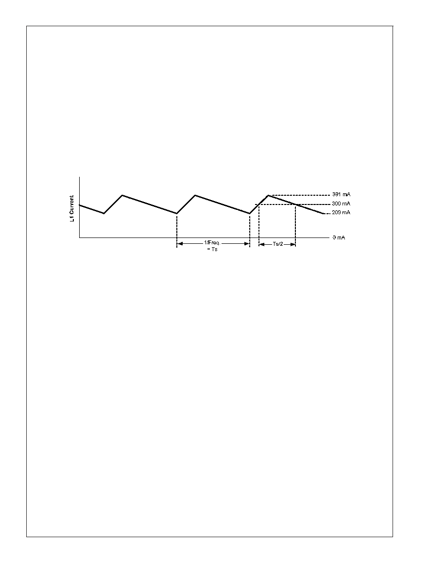
Starting when the current reaches Io (300 mA in Figure 12)
half way through the on-time, the current continues to in-
crease to the peak (391 mA), and then decreases to 300 mA
half way through the off-time. The average value of this
portion of the waveform is 45.5mA, and will cause half of the
voltage ripple, or 14 mV. The interval is one half of the
frequency cycle time, or 2.23 µs. Using the capacitor's basic
equation:
C = I x
t / V
the minimum value for C2 is 7.2 µF. The ripple due to C2's
capacitance is 90∞ out of phase from the ESR ripple, and the
two numbers do not add directly. However, this calculation
provides a practical minimum value for C2 based on its ESR,
and the target spec. To allow for the capacitor's tolerance,
temperature effects, and voltage effects, a 15 µF, X7R ca-
pacitor will be used.
c) In summary: The above calculations provide a minimum
value for C2, and a calculation for R3. The ESR is just as
important as the capacitance. The calculated values are
guidelines, and should be treated as starting points. For
each application, experimentation is needed to determine
the optimum values for R3 and C2.
R
CL
: When a current limit condition is detected, the minimum
off-time set by this resistor must be greater than the maxi-
mum normal off-time which occurs at maximum Vin. Using
equation 2, the minimum on-time is 0.470 µs, yielding a
maximum off-time of 3.99 µs. This is increased by 117 ns (to
4.11 µs) due to a
±
25% tolerance of the on-time. This value
is then increased to allow for:
The response time of the current limit detection loop
(400ns),
The off-time determined by equation 3 has a
±
25% toler-
ance,
t
OFFCL(MIN)
= (4.11 µs + 0.40µs) x 1.25 = 5.64 µs
Using equation 3, R
CL
calculates to 264k
(at V
FB
= 2.5V).
The closest standard value is 267 k
.
D1: The important parameters are reverse recovery time and
forward voltage. The reverse recovery time determines how
long the reverse current surge lasts each time the buck
switch is turned on. The forward voltage drop is significant in
the event the output is short-circuited as it is only this diode's
voltage which forces the inductor current to reduce during
the forced off-time. For this reason, a higher voltage is better,
although that affects efficiency. A good choice is an ultrafast
power diode, such as the MURA110T3 from ON Semicon-
ductor. Its reverse recovery time is 30ns, and its forward
voltage drop is approximately 0.72V at 300 mA at 25∞C.
Other types of diodes may have a lower forward voltage
drop, but may have longer recovery times, or greater reverse
leakage. D1's reverse voltage rating must be at least as
great as the maximum Vin, and its current rating be greater
than the maximum current limit threshold (610 mA).
C1: This capacitor's purpose is to supply most of the switch
current during the on-time, and limit the voltage ripple at Vin,
on the assumption that the voltage source feeding Vin has
an output impedance greater than zero. At maximum load
current, when the buck switch turns on, the current into pin 8
will suddenly increase to the lower peak of the output current
waveform, ramp up to the peak value, then drop to zero at
turn-off. The average input current during this on-time is the
load current (300 mA). For a worst case calculation, C1 must
20097926
FIGURE 12. Inductor Current Waveform
LM5008
www.national.com
11
Applications Information
(Continued)
supply this average load current during the maximum on-
time. To keep the input voltage ripple to less than 2V (for this
exercise), C1 calculates to:
Quality ceramic capacitors in this value have a low ESR
which adds only a few millivolts to the ripple. It is the capaci-
tance which is dominant in this case. To allow for the capaci-
tor's tolerance, temperature effects, and voltage effects, a
1.0 µF, 100V, X7R capacitor will be used.
C4: The recommended value is 0.01µF for C4, as this is
appropriate in the majority of applications. A high quality
ceramic capacitor, with low ESR is recommended as C4
supplies the surge current to charge the buck switch gate at
turn-on. A low ESR also ensures a quick recharge during
each off-time. At minimum Vin, when the on-time is at maxi-
mum, it is possible during start-up that C4 will not fully
recharge during each 300 ns off-time. The circuit will not be
able to complete the start-up, and achieve output regulation.
This can occur when the frequency is intended to be low
(e.g., R
ON
= 500K). In this case C4 should be increased so
it can maintain sufficient voltage across the buck switch
driver during each on-time.
C5: This capacitor helps avoid supply voltage transients and
ringing due to long lead inductance at V
IN
. A low ESR, 0.1µF
ceramic chip capacitor is recommended, located close to the
LM5008.
FINAL CIRCUIT
The final circuit is shown in Figure 13. The circuit was tested,
and the resulting performance is shown in Figure 6 through
Figure 8 .
PC BOARD LAYOUT
The LM5008 regulation and over-voltage comparators are
very fast, and as such will respond to short duration noise
pulses. Layout considerations are therefore critical for opti-
mum performance. The components at pins 1, 2, 3, 5, and 6
should be as physically close as possible to the IC, thereby
minimizing noise pickup in the PC tracks. The current loop
formed by D1, L1, and C2 should be as small as possible.
The ground connection from C2 to C1 should be as short
and direct as possible.
If the internal dissipation of the LM5008 produces excessive
junction temperatures during normal operation, good use of
the pc board's ground plane can help considerably to dissi-
pate heat. The exposed pad on the bottom of the LLP-8
package can be soldered to a ground plane on the PC board,
and that plane should extend out from beneath the IC to help
dissipate the heat. Additionally, the use of wide PC board
traces, where possible, can also help conduct heat away
from the IC. Judicious positioning of the PC board within the
end product, along with use of any available air flow (forced
or natural convection) can help reduce the junction
temperatures.
20097922
FIGURE 13. LM5008 Example Circuit
LM5008
www.national.com
12
Applications Information
(Continued)
Bill of Materials (Circuit of Figure 13)
Item
Description
Part Number
Value
C1
Ceramic Capacitor
TDK C4532X7R2A105M
1µF, 100V
C2
Ceramic Capacitor
TDK C4532X7R1E156M
15µF, 25V
C3
Ceramic Capacitor
Kemet C1206C104K5RAC
0.1µF, 50V
C4
Ceramic Capacitor
Kemet C1206C103K5RAC
0.01µF, 50V
C5
Ceramic Capacitor
TDK C3216X7R2A104M
0.1µF, 100V
D1
UltraFast Power Diode
ON Semi MURA110T3
100V, 1A
L1
Power Inductor
Coilcraft DO3316-224 or
220 µH
TDK SLF10145T-221MR65
R1
Resistor
Vishay CRCW12063011F
3.01 k
R2
Resistor
Vishay CRCW12061001F
1.0 k
R3
Resistor
Vishay CRCW12062R00F
2.0
R
ON
Resistor
Vishay CRCW12063573F
357 k
R
CL
Resistor
Vishay CRCW12062673F
267 k
U1
Switching Regulator
National Semiconductor LM5008
LM5008
www.national.com
13
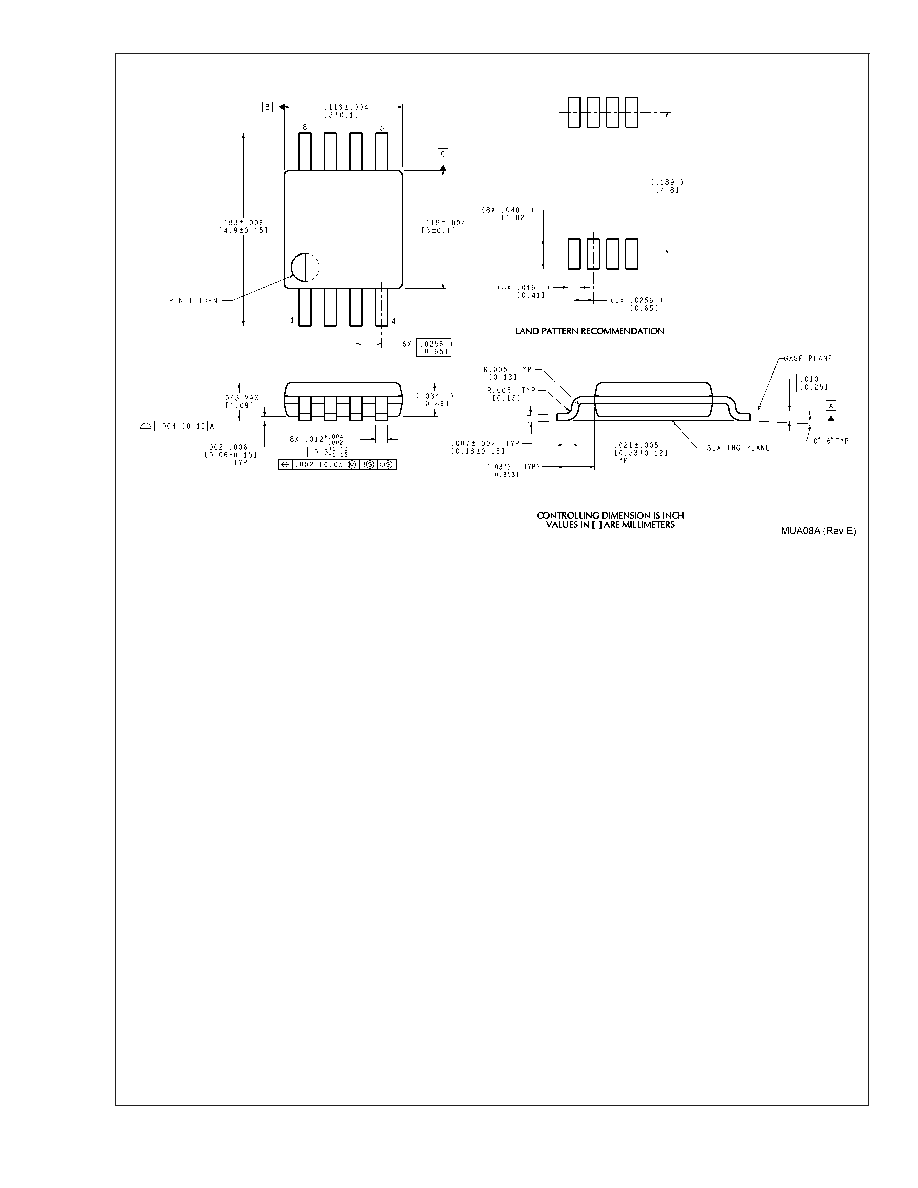
Physical Dimensions
inches (millimeters) unless otherwise noted
8-Lead MSOP Package
NS Package Number MUA08A
LM5008
www.national.com
14
Physical Dimensions
inches (millimeters) unless otherwise noted (Continued)
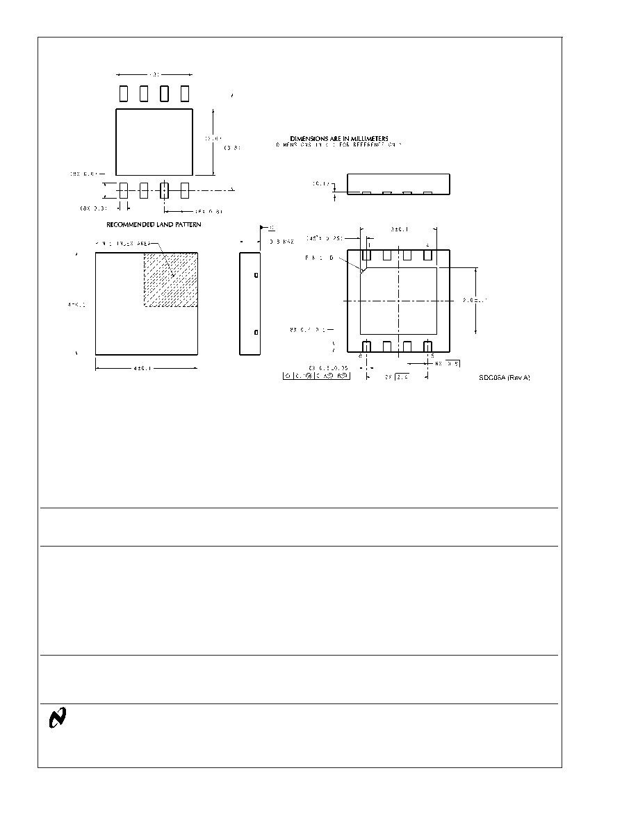
8-Lead LLP Package
NS Package Number SDC08A
National does not assume any responsibility for use of any circuitry described, no circuit patent licenses are implied and National reserves
the right at any time without notice to change said circuitry and specifications.
For the most current product information visit us at www.national.com.
LIFE SUPPORT POLICY
NATIONAL'S PRODUCTS ARE NOT AUTHORIZED FOR USE AS CRITICAL COMPONENTS IN LIFE SUPPORT DEVICES OR SYSTEMS
WITHOUT THE EXPRESS WRITTEN APPROVAL OF THE PRESIDENT AND GENERAL COUNSEL OF NATIONAL SEMICONDUCTOR
CORPORATION. As used herein:
1. Life support devices or systems are devices or systems
which, (a) are intended for surgical implant into the body, or
(b) support or sustain life, and whose failure to perform when
properly used in accordance with instructions for use
provided in the labeling, can be reasonably expected to result
in a significant injury to the user.
2. A critical component is any component of a life support
device or system whose failure to perform can be reasonably
expected to cause the failure of the life support device or
system, or to affect its safety or effectiveness.
BANNED SUBSTANCE COMPLIANCE
National Semiconductor certifies that the products and packing materials meet the provisions of the Customer Products Stewardship
Specification (CSP-9-111C2) and the Banned Substances and Materials of Interest Specification (CSP-9-111S2) and contain no ``Banned
Substances'' as defined in CSP-9-111S2.
National Semiconductor
Americas Customer
Support Center
Email: new.feedback@nsc.com
Tel: 1-800-272-9959
National Semiconductor
Europe Customer Support Center
Fax: +49 (0) 180-530 85 86
Email: europe.support@nsc.com
Deutsch Tel: +49 (0) 69 9508 6208
English
Tel: +44 (0) 870 24 0 2171
FranÁais Tel: +33 (0) 1 41 91 8790
National Semiconductor
Asia Pacific Customer
Support Center
Email: ap.support@nsc.com
National Semiconductor
Japan Customer Support Center
Fax: 81-3-5639-7507
Email: jpn.feedback@nsc.com
Tel: 81-3-5639-7560
www.national.com
LM5008
High
V
oltage
(100V)
Step
Down
Switching
Regulator