 | –≠–ª–µ–∫—Ç—Ä–æ–Ω–Ω—ã–π –∫–æ–º–ø–æ–Ω–µ–Ω—Ç: LM5009MMX | –°–∫–∞—á–∞—Ç—å:  PDF PDF  ZIP ZIP |
LM5009
150 mA, 100V Step-Down Switching Regulator
General Description
The LM5009 Step Down Switching Regulator features all of
the functions needed to implement a low cost, efficient, Buck
bias regulator. This device is capable of driving a 150 mA
load current from a 9.5V to 95V input source. The switching
frequency can exceed 600 kHz, depending on the input and
output voltages. The output voltage may be set from 2.5V to
85V. This high voltage regulator contains an N-Channel buck
switch and internal startup regulator. The device is easy to
implement and is provided in the MSOP-8 and the thermally
enhanced LLP-8 packages. The LM5009 is a well suited
alternative to a high voltage monolithic or discrete linear
solution where the power loss becomes unacceptable. The
regulator's operation is based on a hysteretic control
scheme using an ON time inversely proportional to VIN. This
feature allows the operating frequency to remain relatively
constant over load and input voltage variations. The hyster-
etic control requires no loop compensation, resulting in an
ultra-fast transient response. An intelligent current limit is
implemented with forced OFF time, which is inversely pro-
portional to Vout. This scheme ensures short circuit protec-
tion while providing minimum foldback. Other features in-
clude: Thermal Shutdown, Vcc under-voltage lockout, Gate
drive under-voltage lockout, and Maximum Duty Cycle lim-
iter.
Features
n
Integrated N-Channel MOSFET
n
Guaranteed 150 mA output current capability
n
Ultra-Fast Transient Response
n
No loop compensation required
n
Vin feed forward provides constant operating frequency
n
Switching frequency can exceed 600 kHz
n
Highly efficient operation
n
2% accurate 2.5V feedback from -40∞C to 125∞C
n
Internal startup regulator
n
Intelligent current limit protection
n
External shutdown control
n
Thermal shutdown
n
MSOP-8 and thermally enhanced LLP packages
Typical Applications
n
Heat sink eliminator for classic linear regulator
applications
n
12V, 24V, 36V, and 48V rectified AC systems
n
42V Automotive
n
Non-isolated AC mains charge coupled supplies
n
LED Current Source
Package
n
MSOP - 8
n
LLP - 8 (4mm x 4mm) (Available Soon)
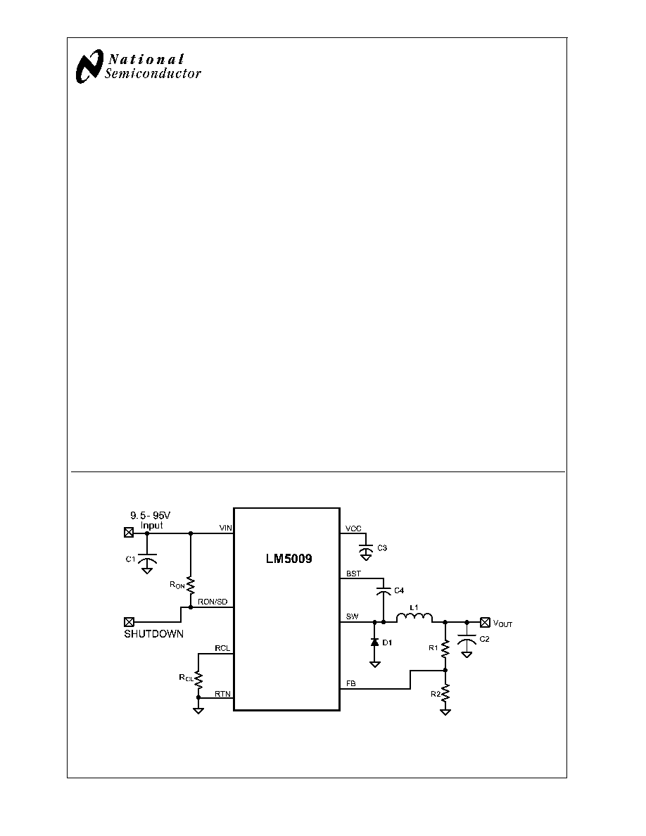
Typical Application Circuit
20165828
Basic Stepdown Regulator
February 2006
LM5009
150
mA,
100V
Step-Down
Switching
Regulator
© 2006 National Semiconductor Corporation
DS201658
www.national.com
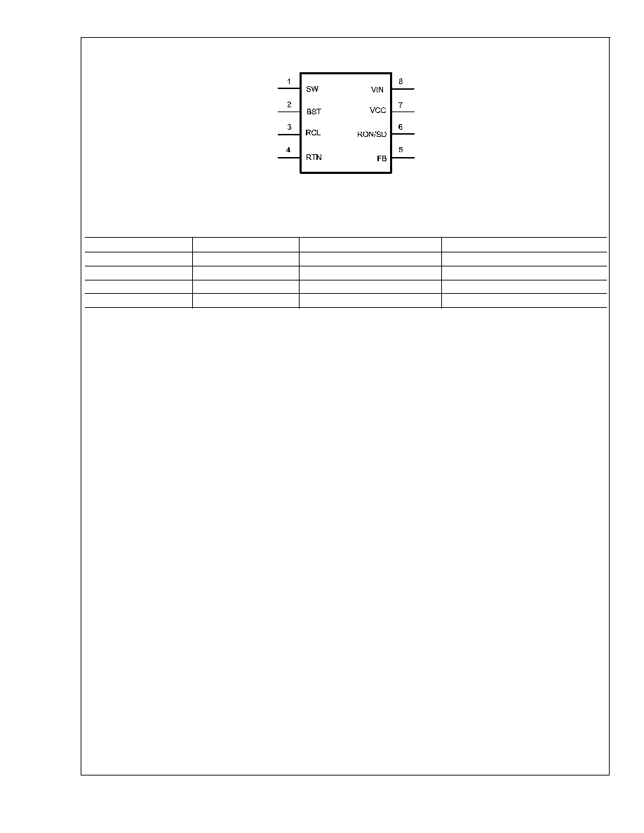
Connection Diagram
20165802
8-Lead MSOP, LLP
Ordering Information
Order Number
Package Type
NSC Package Drawing
Supplied As
LM5009MM
MSOP-8
MUA08A
1000 Units on Tape and Reel
LM5009MMX
MSOP-8
MUA08A
3500 Units per Reel
LM5009SD
LLP-8
Available Soon
LM5009SDX
LLP-8
Available Soon
LM5009
www.national.com
2
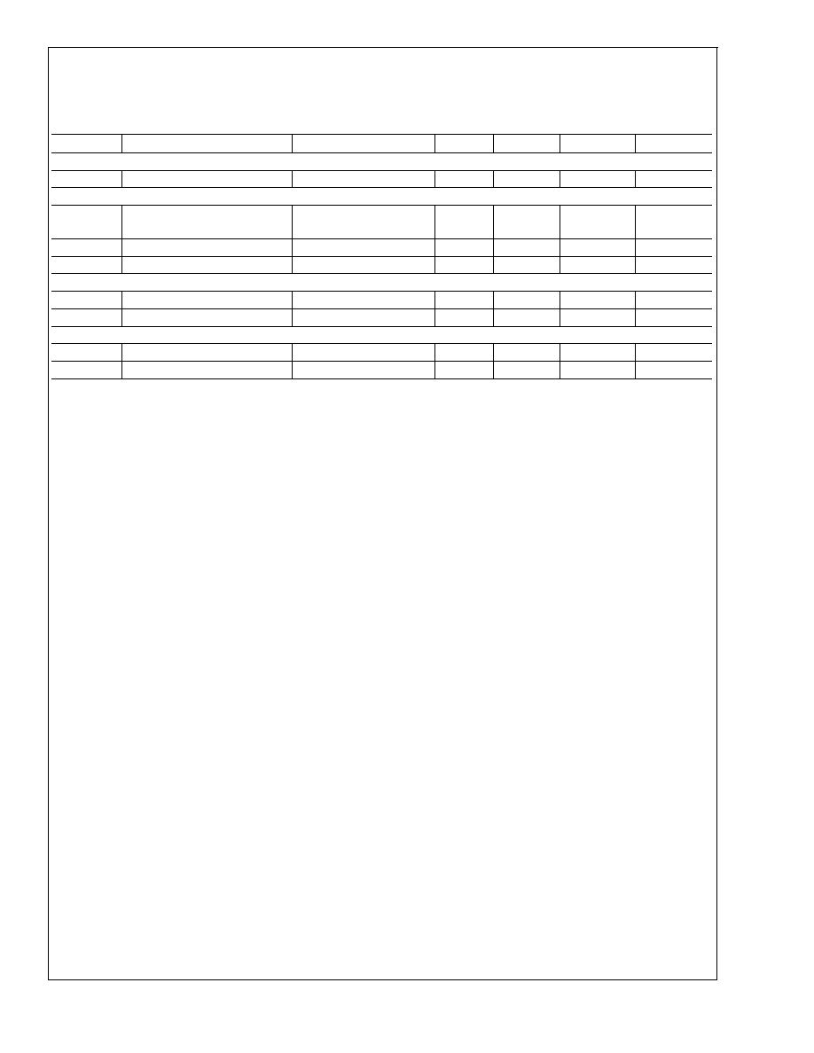
Pin Descriptions
Pin
Name
Description
Application Information
1
SW
Switching output
Power switching output. Connect to the inductor,
re-circulating diode, and bootstrap capacitor.
2
BST
Boost Pin
An external capacitor is required between the BST
and the SW pins. A 0.01µF ceramic capacitor is
recommended. An internal diode charges the
capacitor from V
CC
.
3
RCL
Current Limit off-time set pin
A resistor between this pin and RTN sets the
off-time when current limit is detected. The off-time
is preset to 35µs if FB = 0V.
4
RTN
Ground pin
Ground for the entire circuit.
5
FB
Feedback input from Regulated Output
This pin is connected to the inverting input of the
internal regulation comparator. The regulation
threshold is 2.5V.
6
RON/SD
On-time set pin
A resistor between this pin and VIN sets the switch
on-time as a function of V
IN
. The minimum
recommended on-time is 250ns at the maximum
input voltage. This pin can be used for remote
shutdown.
7
VCC
Output from the internal high voltage startup
regulator. Regulated at 7.0V.
If an auxiliary voltage is available to raise the
voltage on this pin above the regulation setpoint
(7V), the internal series pass regulator will
shutdown, reducing the IC power dissipation. Do not
exceed 14V. This voltage provides gate drive power
for the internal Buck switch. An internal diode is
provided between this pin and the BST pin. A local
0.1µF decoupling capacitor is required.
8
VIN
Input voltage
Recommended operating range: 9.5V to 95V.
EP
Exposed Pad (LLP Package only)
Exposed metal pad on the underside of the device.
It is recommended to connect this to the PC board
ground plane to aid in heat dissipation.
LM5009
www.national.com
3
Absolute Maximum Ratings
(Note 1)
If Military/Aerospace specified devices are required,
please contact the National Semiconductor Sales Office/
Distributors for availability and specifications.
V
IN
to RTN
-0.3V to 100V
BST to RTN
-0.3V to 114V
SW to RTN (Steady State)
-1V
ESD Rating (Note 5)
Human Body Model
2kV
BST to VCC
100V
BST to SW
14V
VCC to RTN
14V
All Other Inputs to RTN
-0.3 to 7V
Storage Temperature Range
-65∞C to +150∞C
Operating Ratings
(Note 1)
V
IN
9.5V to 95V
Operating Junction Temperature
-40∞C to + 125∞C
Electrical Characteristics
Limits in standard type are for T
J
= 25∞C only, and limits in boldface type apply over the junction temperature (T
J
) range of
-40∞C to +125∞C. Minimum and Maximum limits are guaranteed through test, design, or statistical correlation. Typical values
represent the most likely parametric norm at T
J
= 25∞C, and are provided for reference purposes only. Unless otherwise stated,
the following conditions apply: V
IN
= 48V, R
ON
= 200k
. See (Note 3)
Symbol
Parameter
Conditions
Min
Typ
Max
Units
V
CC
Supply
V
CC
Reg
V
CC
Regulator Output
6.6
7
7.4
V
V
CC
Current Limit
(Note 4)
9.5
mA
V
CC
undervoltage Lockout
Voltage (V
CC
increasing)
6.3
V
V
CC
Undervoltage Hysteresis
200
mV
V
CC
UVLO Delay (filter)
100mV overdrive
10
µs
I
IN
Operating Current
Non-Switching, FB = 3V
485
675
µA
I
IN
Shutdown Current
RON/SD = 0V
76
150
µA
Switch Characteristics
Buck Switch Rds(on)
I
TEST
= 200mA, (Note 6)
2.0
4.4
Gate Drive UVLO
V
BST
- V
SW
Rising
3.4
4.5
5.5
V
Gate Drive UVLO Hysteresis
430
mV
Current Limit
Current Limit Threshold
0.25
0.31
0.37
A
Current Limit Response Time
I
switch
Overdrive = 0.1A
Time to Switch Off
400
ns
OFF time generator (test 1)
FB=0V, R
CL
= 100K
35
µs
OFF time generator (test 2)
FB=2.3V, R
CL
= 100K
2.56
µs
On Time Generator
T
ON
- 1
Vin = 10V
Ron = 200K
2.15
2.77
3.5
µs
T
ON
- 2
Vin = 95V
Ron = 200K
200
300
420
ns
Remote Shutdown Threshold
Rising
0.40
0.70
1.05
V
Remote Shutdown Hysteresis
35
mV
LM5009
www.national.com
4
Electrical Characteristics
(Continued)
Limits in standard type are for T
J
= 25∞C only, and limits in boldface type apply over the junction temperature (T
J
) range of
-40∞C to +125∞C. Minimum and Maximum limits are guaranteed through test, design, or statistical correlation. Typical values
represent the most likely parametric norm at T
J
= 25∞C, and are provided for reference purposes only. Unless otherwise stated,
the following conditions apply: V
IN
= 48V, R
ON
= 200k
. See (Note 3)
Symbol
Parameter
Conditions
Min
Typ
Max
Units
Minimum Off Time
Minimum Off Timer
FB = 0V
300
ns
Regulation and OV Comparators
FB Reference Threshold
Internal reference
Trip point for switch ON
2.445
2.5
2.550
V
FB Over-Voltage Threshold
Trip point for switch OFF
2.875
V
FB Bias Current
1
nA
Thermal Shutdown
Tsd
Thermal Shutdown Temp.
165
∞C
Thermal Shutdown Hysteresis
25
∞C
Thermal Resistance
JA
Junction to Ambient
MUA Package
200
∞C/W
SDC Package
∞C/W
Note 1: Absolute Maximum Ratings are limits beyond which damage to the device may occur. Operating Ratings are conditions under which operation of the device
is intended to be functional. For guaranteed specifications and test conditions, see the Electrical Characteristics.
Note 2: For detailed information on soldering plastic MSOP and LLP packages, refer to the Packaging Data Book available from National Semiconductor
Corporation.
Note 3: All limits are guaranteed. All electrical characteristics having room temperature limits are tested during production with T
A
= T
J
= 25∞C. All hot and cold limits
are guaranteed by correlating the electrical characteristics to process and temperature variations and applying statistical process control.
Note 4: The V
CC
output is intended as a self bias for the internal gate drive power and control circuits. Device thermal limitations limit external loading.
Note 5: The human body model is a 100pF capacitor discharged through a 1.5k
resistor into each pin. All pins are rated for 2 kV, except VIN and VCC which are
rated for 1 kV.
Note 6: For devices procured in the LLP-8 package the Rds(on) limits are guaranteed by design characterization data only.
LM5009
www.national.com
5