 | ÐлекÑÑоннÑй компоненÑ: LM5010A | СкаÑаÑÑ:  PDF PDF  ZIP ZIP |
LM5010A High Voltage 1A Step Down Switching Regulator
LM5010A
High Voltage 1A Step Down Switching Regulator
General Description
The LM5010A Step Down Switching Regulator is an en-
hanced version of the LM5010 with the input operating range
extended to 6V minimum. The LM5010A features all the
functions needed to implement a low cost, efficient, buck
regulator capable of supplying in excess of 1A load current.
This high voltage regulator integrates an N-Channel Buck
Switch, and is available in thermally enhanced LLP-10 and
TSSOP-14EP packages. The constant on-time regulation
scheme requires no loop compensation resulting in fast load
transient response and simplified circuit implementation. The
operating frequency remains constant with line and load
variations due to the inverse relationship between the input
voltage and the on-time. The valley current limit detection is
set at 1.25A. Additional features include: VCC under-voltage
lock-out, thermal shutdown, gate drive under-voltage lock-
out, and maximum duty cycle limiter.
Features
n
Wide 6V to 75V Input Voltage Range
n
Valley Current Limiting At 1.25A
n
Programmable Switching Frequency Up To 1 MHz
n
Integrated 80V N-Channel Buck Switch
n
Integrated High Voltage Bias Regulator
n
No Loop Compensation Required
n
Ultra-Fast Transient Response
n
Nearly Constant Operating Frequency With Line and
Load Variations
n
Adjustable Output Voltage
n
2.5V,
±
2% Feedback Reference
n
Programmable Soft-Start
n
Thermal shutdown
Typical Applications
n
Non-Isolated Telecommunications Regulator
n
Secondary Side Post Regulator
n
Power SUpply for Automotive Electronics
Package
n
LLP-10 (4 mm x 4 mm)
n
TSSOP-14EP
n
Both Packages Have Exposed Thermal Pad For
Improved Heat Dissipation
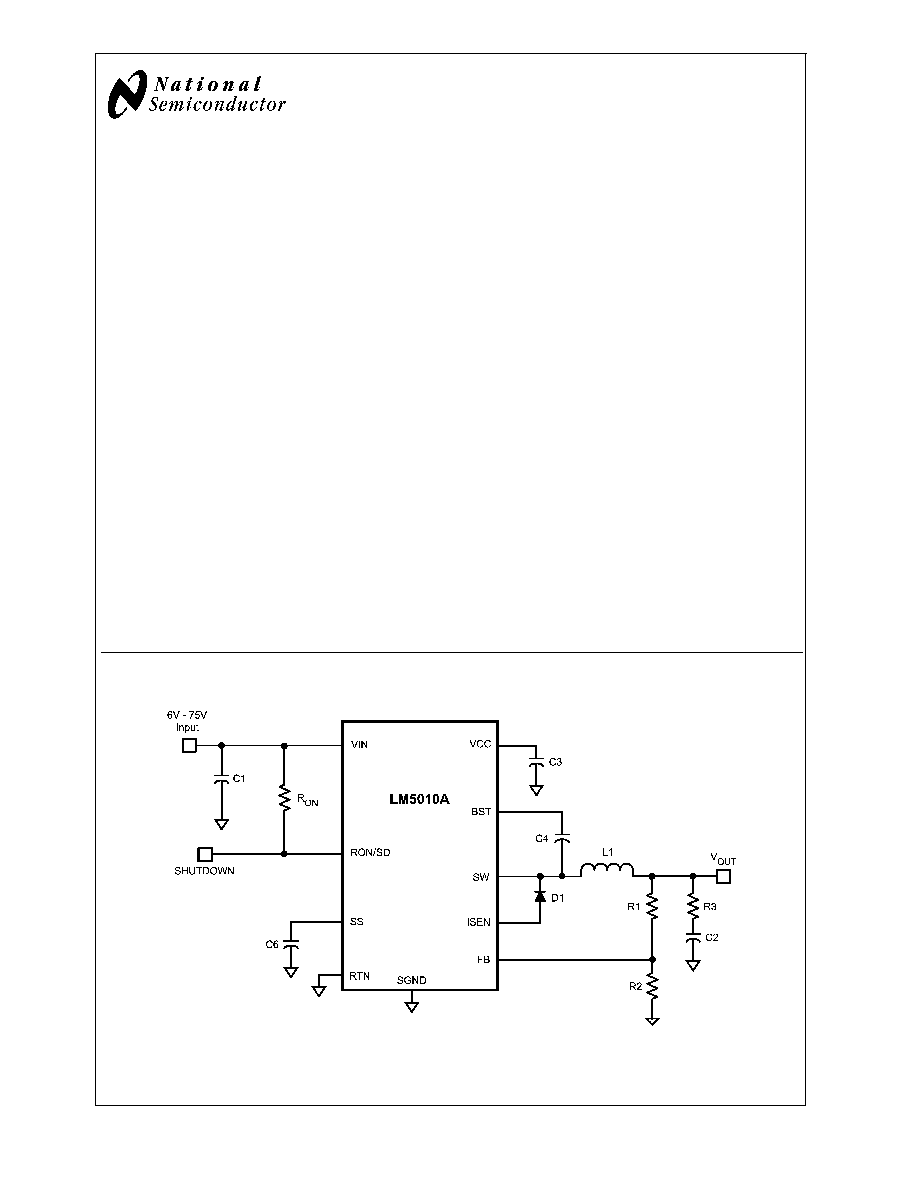
Basic Step Down Regulator
20153843
October 2005
LM5010A
High
V
oltage
1A
Step
Down
Switching
Regulator
© 2005 National Semiconductor Corporation
DS201538
www.national.com

Connection Diagrams
20153802
20153803
Ordering Information
Order Number
Package Type
NSC Package
Drawing
Junction Temperature
Range
Supplied As
LM5010ASD
LLP-10 (4x4)
SDC10A
-40°C to + 125°C
1000 Units on Tape and Reel
LM5010ASDX
LLP-10 (4x4)
SDC10A
-40°C to + 125°C
4500 Units on Tape and Reel
LM5010AMH
TSSOP-14EP
MXA14A
-40°C to + 125°C
94 Units in Rail
LM5010AMHX
TSSOP-14EP
MXA14A
-40°C to + 125°C
2500 Units on Tape and Reel
LM5010AHMH
TSSOP-14EP
MXA14A
-40°C to + 150°C
Available Soon
LM5010AHMHX
TSSOP-14EP
MXA14A
-40°C to + 150°C
Available Soon
LM5010A
www.national.com
2
Pin Descriptions
Pin Number
Name
Description
Application Information
LLP-10
TSSOP-14
1
2
SW
Switching Node
Internally connected to the buck switch source.
Connect to the inductor, free-wheeling diode, and
bootstrap capacitor.
2
3
BST
Boost pin for bootstrap capacitor
Connect a capacitor from SW to the BST pin. The
capacitor is charged from VCC via an internal diode
during the buck switch off-time.
3
4
ISEN
Current sense
During the buck switch off-time, the inductor current
flows through the internal sense resistor, and out of
the ISEN pin to the free-wheeling diode. The current
limit comparator keeps the buck switch off if the
ISEN current exceeds 1.25A (typical).
4
5
SGND
Current Sense Ground
Re-circulating current flows into this pin to the
current sense resistor.
5
6
RTN
Circuit Ground
Ground return for all internal circuitry other than the
current sense resistor.
6
9
FB
Voltage feedback input from the
regulated output
Input to both the regulation and over-voltage
comparators. The FB pin regulation level is 2.5V.
7
10
SS
Softstart
An internal 11.5 µA current source charges the SS
pin capacitor to 2.5V to soft-start the reference input
of the regulation comparator.
8
11
RON/SD
On-time control and shutdown
An external resistor from VIN to the RON/SD pin
sets the buck switch on-time. Grounding this pin
shuts down the regulator.
9
12
VCC
Output of the bias regulator
The voltage at VCC is nominally equal to V
IN
for V
IN
<
8.9V, and regulated at 7V for V
IN
>
8.9V.
Connect a 0.47 µF, or larger capacitor from VCC to
ground, as close as possible to the pins. An external
voltage can be applied to this pin to reduce internal
dissipation if V
IN
is greater than 8.9V. MOSFET
body diodes clamp VCC to VIN if V
CC
>
V
IN
.
10
13
VIN
Input supply voltage
Nominal input range is 6V to 75V. Input bypass
capacitors should be located as close as possible to
the VIN pin and RTN pins.
1,7,8,14
NC
No connection.
No internal connection. Can be connected to ground
plane to improve heat dissipation.
EP
Exposed Pad
Exposed metal pad on the underside of the device.
It is recommended to connect this pad to the PC
board ground plane to aid in heat dissipation.
LM5010A
www.national.com
3
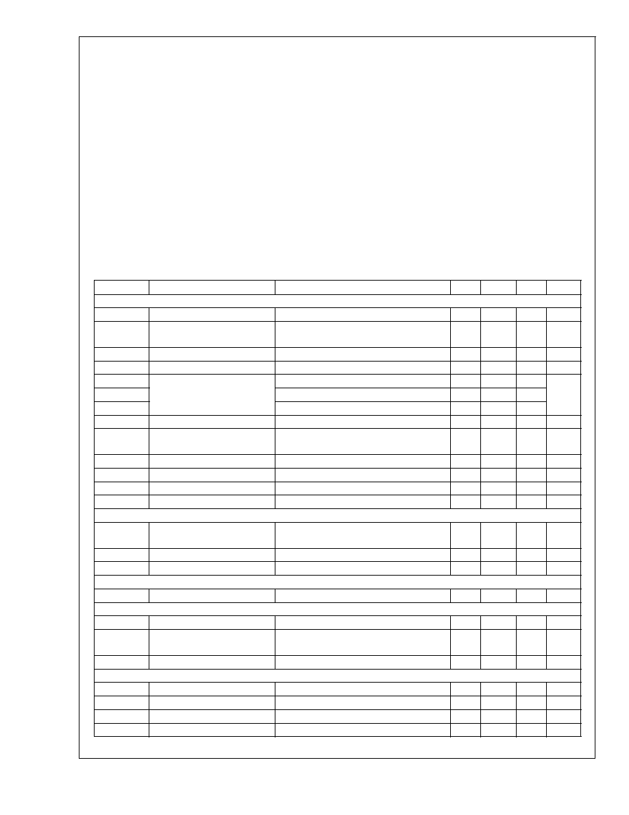
Absolute Maximum Ratings
(Note 1)
If Military/Aerospace specified devices are required,
please contact the National Semiconductor Sales Office/
Distributors for availability and specifications.
VIN to RTN
-0.3V to 76V
BST to RTN
-0.3V to 90V
SW to RTN (Steady State)
-1.5V
BST to VCC
76V
BST to SW
14V
VCC to RTN
-0.3V to 14V
SGND to RTN
-0.3V to +0.3V
SS to RTN
-0.3V to 4V
VIN to SW
76V
All Other Inputs to RTN
-0.3V to 7V
ESD Rating (Note 2)
Human Body Model
2kV
Storage Temperature Range
-65°C to +150°C
Lead Temperature (Soldering 4 sec) (Note 4)
260°C
Operating Ratings
(Note 1)
VIN Voltage
6.0V to 75V
Junction Temperature
LM5010A
-40°C to + 125°C
LM5010AH
-40°C to + 150°C
Electrical Charateristics
Specifications with standard type are for T
J
= 25°C only; limits in boldface type ap-
ply over the full Operating Junction Temperature (T
J
) range. Minimum and Maximum limits are guaranteed through test, de-
sign, or statistical correlation. Typical values represent the most likely parametric norm at T
J
= 25°C, and are provided for ref-
erence purposes only. Unless otherwise stated the following conditions apply: V
IN
= 48V, R
ON
= 200k
. See (Note 5).
Symbol
Parameter
Conditions
Min
Typ
Max
Units
V
CC
Regulator
V
CC
Reg
V
CC
regulated output
6.6
7
7.4
Volts
V
IN
- V
CC
I
CC
= 0 mA, F
S
<
200 kHz, 6.0V
V
IN
8.5V
100
mV
V
CC
Bypass Threshold
V
IN
Increasing
8.9
V
V
CC
Bypass Hysteresis
V
IN
Decreasing
260
mV
V
CC
output impedance
(0 mA
I
CC
5 mA)
V
IN
= 6.0V
55
V
IN
= 8.0V
50
V
IN
= 48V
0.21
V
CC
current limit (Note 3)
V
IN
= 48V, V
CC
= 0V
15
mA
UVLOVcc
V
CC
under-voltage lock-out
threshold
V
CC
Increasing
5.25
V
UVLO
VCC
hysteresis
V
CC
Decreasing
180
mV
UVLO
VCC
filter delay
100 mV overdrive
3
µs
I
IN
operating current
Non-switching, FB = 3V
675
950
µA
I
IN
shutdown current
RON/SD = 0V
100
200
µA
Switch Characteristics
R
DS(on)
Buck Switch R
DS(on)
@
I
SW
=
200 mA
T
J
125°C
T
J
150°C
0.35
0.80
0.85
UVLO
GD
Gate Drive UVLO
V
BST
- V
SW
Increasing
1.7
3.0
4.0
V
UVLO
GD
hysteresis
400
mV
SOFT-START Pin
I
SS
Internal current source
8.0
11.5
15
µA
Current Limit
I
LIM
Threshold
Current out of I
SEN
1
1.25
1.5
A
Resistance from ISEN to
SGND
130
m
Response time
150
ns
On Timer, RON/SD Pin
t
ON
- 1
On-time
V
IN
= 10V, R
ON
= 200 k
2.1
2.75
3.4
µs
t
ON
- 2
On-time
V
IN
= 75V, R
ON
= 200 k
290
390
496
ns
Shutdown threshold
Voltage at RON/SD rising
0.30
0.7
1.05
V
Threshold hysteresis
40
mV
LM5010A
www.national.com
4
Electrical Charateristics
Specifications with standard type are for T
J
= 25°C only; limits in boldface type apply
over the full Operating Junction Temperature (T
J
) range. Minimum and Maximum limits are guaranteed through test, design,
or statistical correlation. Typical values represent the most likely parametric norm at T
J
= 25°C, and are provided for reference
purposes only. Unless otherwise stated the following conditions apply: V
IN
= 48V, R
ON
= 200k
. See (Note 5). (Continued)
Symbol
Parameter
Conditions
Min
Typ
Max
Units
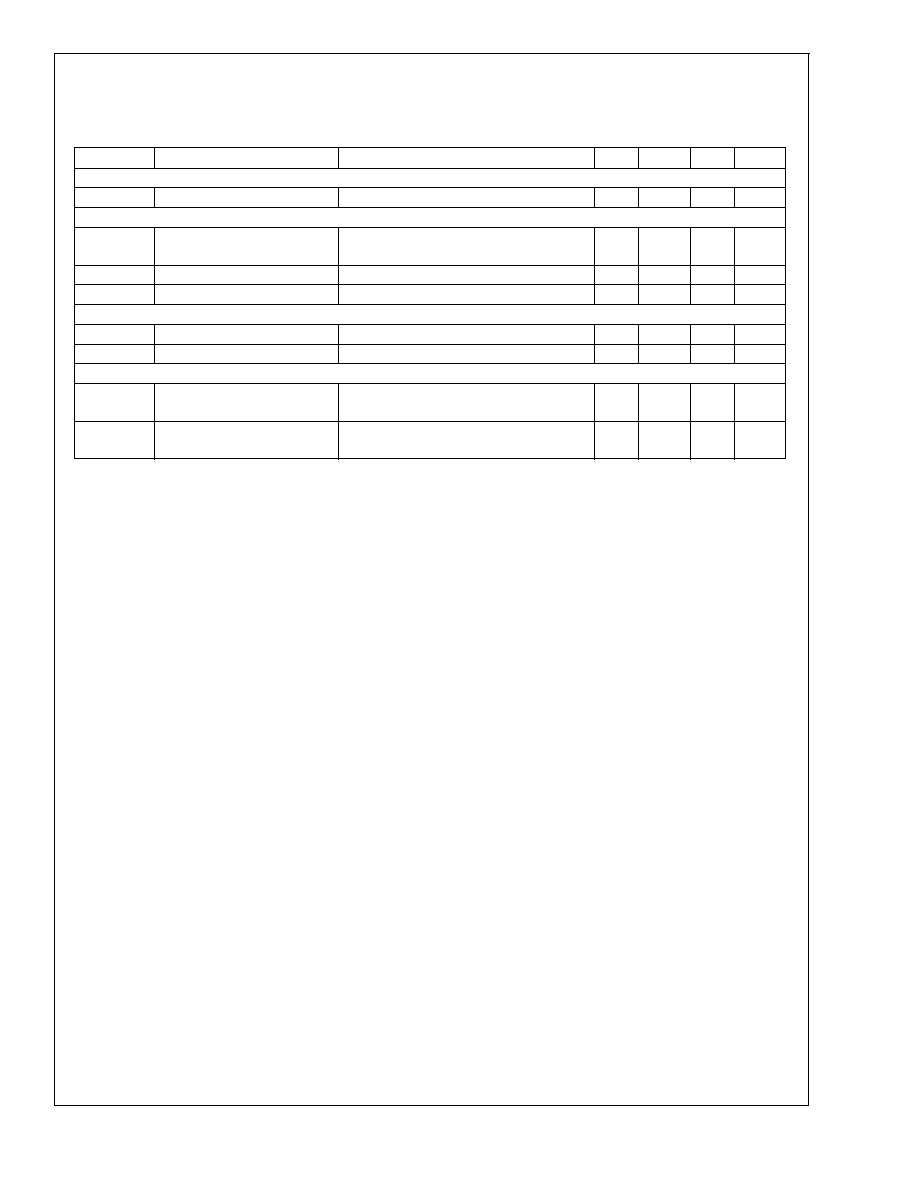
Off Timer
t
OFF
Minimum Off-time
260
ns
Regulation and Over-Voltage Comparators (FB Pin)
V
REF
FB regulation threshold
T
J
125°C
T
J
150°C
2.445
2.435
2.50
2.550
V
FB over-voltage threshold
2.9
V
FB bias current
1
nA
Thermal Shutdown
T
SD
Thermal shutdown temperature
175
°C
Thermal shutdown hysteresis
20
°C
Thermal Resistance
JA
Junction to Ambient, 0 LFPM
Air Flow
SDC Package
MXA Package
40
40
°C/W
JC
Junction to Case
SDC Package
MXA Package
5.2
5.2
°C/W
Note 1: Absolute Maximum Ratings are limits beyond which damage to the device may occur. Operating Ratings are conditions under which operation of the device
is intended to be functional. For guaranteed specifications and test conditions, see the Electrical Characteristics.
Note 2: The human body model is a 100pF capacitor discharged through a 1.5k
resistor into each pin.
Note 3: V
CC
provides bias for the internal gate drive and control circuits. Device thermal limitations limit external loading.
Note 4: For detailed information on soldering plastic TSSOP and LLP packages refer to the Packaging Data Book available from National Semiconductor
Corporation.
Note 5: Typical specifications represent the most likely parametric norm at 25°C operation.
LM5010A
www.national.com
5
Document Outline