LM5025
Active Clamp Voltage Mode PWM Controller
General Description
The LM5025 PWM controller contains all of the features
necessary to implement power converters utilizing the Active
Clamp / Reset technique. The device can be configured to
control either a P-Channel clamp switch or an N-Channel
clamp switch. With the active clamp technique, higher effi-
ciencies and greater power densities can be realized com-
pared to conventional catch winding or RDC clamp / reset
techniques. Two control outputs are provided, the main
power switch control (OUT_A) and the active clamp switch
control (OUT_B). The active clamp output can be configured
for either a guaranteed overlap time (for P-Channel switch
applications) or a guaranteed deadtime (for N_Channel ap-
plications). The two internal compound gate drivers parallel
both MOS and Bipolar devices, providing superior gate drive
characteristics. This controller is designed for high-speed
operation including an oscillator frequency range up to 1MHz
and total PWM and current sense propagation delays less
than 100ns. The LM5025 includes a high-voltage start-up
regulator that operates over a wide input range of 13V to
90V. Additional features include: Line Under Voltage Lockout
(UVLO), softstart, oscillator UP/DOWN sync capability, pre-
cision reference and thermal shutdown.
Features
n
Internal Start-up Bias Regulator
n
3A Compound Main Gate Driver
n
Programmable Line Under-Voltage Lockout (UVLO) with
Adjustable Hysteresis
n
Voltage Mode Control with Feed-Forward
n
Adjustable Dual Mode Over-Current Protection
n
Programmable Overlap or Deadtime between the Main
and Active Clamp Outputs
n
Volt x Second Clamp
n
Programmable Soft-start
n
Leading Edge Blanking
n
Single Resistor Programmable Oscillator
n
Oscillator UP / DOWN Sync Capability
n
Precision 5V Reference
n
Thermal Shutdown
Packages
n
TSSOP-16
n
LLP-16 (5x5 mm) Thermally Enhanced
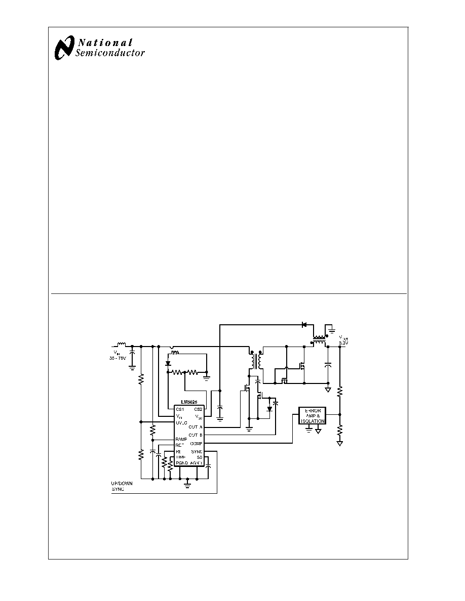
Typical Application Circuit
20086901
Simplified Active Clamp Forward Power Converter
March 2004
LM5025
Active
Clamp
V
oltage
Mode
PWM
Controller
� 2004 National Semiconductor Corporation
DS200869
www.national.com
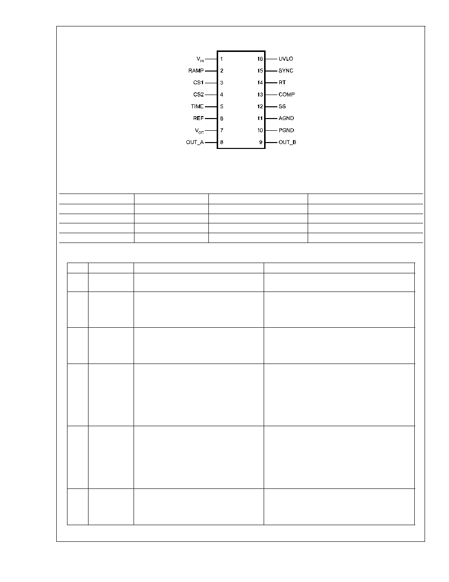
Connection Diagram
20086916
16-Lead TSSOP, LLP
Ordering Information
Order Number
Package Type
NSC Package Drawing
Supplied As
LM5025MTC
TSSOP-16
MTC-16
92 Units per anti-static tube
LM5025MTCX
TSSOP-16
MTC-16
2500 Units on Tape and Reel
LM5025SD
LLP-16
SDA-16A
1000 Units on Tape and Reel
LM5025SDX
LLP-16
SDA-16A
4500 Units on Tape and Reel
Pin Description
PIN
NAME
DESCRIPTION
APPLICATION INFORMATION
1
V
IN
Source Input Voltage
Input to start-up regulator. Input range 13V to 90V,
with transient capability to 100V.
2
RAMP
Modulator ramp signal
An external RC circuit from Vin sets the ramp slope.
This pin is discharged at the conclusion of every
cycle by an internal FET, initiated by either the
internal clock or the V*Sec Clamp comparator.
3
CS1
Current sense input for cycle-by-cycle limiting If CS1 exceeds 0.25V the outputs will go into
Cycle-by-Cycle current limit. CS1 is held low for
50ns after OUT_A switches high providing leading
edge blanking.
4
CS2
Current sense input for soft restart
If CS2 exceeds 0.25V the outputs will be disabled
and a softstart commenced. The soft-start capacitor
will be fully discharged and then released with a
pull-up current of 1�A. After the first output pulse
(when SS =1V), the SS charge current will revert
back to 20�A. CS2 is held low for 50ns after OUT_A
switches high, providing leading edge blanking.
5
TIME
Output overlap/Deadtime control
An external resistor (R
SET
) sets either the overlap
time or dead time for the active clamp output. An
R
SET
resistor connected between TIME and GND
produces in-phase OUT_A and OUT_B pulses with
overlap. An R
SET
resistor connected between TIME
and REF produces out-of-phase OUT_A and OUT_B
pulses with deadtime.
6
REF
Precision 5 volt reference output
Maximum output current: 10mA Locally decouple
with a 0.1�F capacitor. Reference stays low until the
line UVLO and the V
CC
UV comparators are
satisfied.
LM5025
www.national.com
2
Pin Description
(Continued)
PIN
NAME
DESCRIPTION
APPLICATION INFORMATION
7
V
CC
Output from the internal high voltage start-up
regulator. The V
CC
voltage is regulated to
7.6V.
If an auxiliary winding raises the voltage on this pin
above the regulation setpoint, the internal start-up
regulator will shutdown, reducing the IC power
dissipation.
8
OUT_A
Main output driver
Output of the main switch PWM output gate driver.
Output capability of 3A peak sink current.
9
OUT_B
Active Clamp output driver
Output of the Active Clamp switch gate driver.
Capable of 1.25A peak sink current..
10
PGND
Power ground
Connect directly to analog ground.
11
AGND
Analog ground
Connect directly to power ground. For the LLP
package option the exposed pad is electrically
connected to AGND.
12
SS
Soft-start control
An external capacitor and an internal 20�A current
source set the softstart ramp. The SS current source
is reduced to 1uA initially following a CS2
over-current event or an over temperature event.
13
COMP
Input to the Pulse Width Modulator
An internal 5K
resistor pull-up is provided on this
pin. The external opto-coupler sinks current from
COMP to control the PWM duty cycle.
14
RT
Oscillator timing resistor pin
An external resistor connected from RT to ground
sets the internal oscillator frequency.
15
SYNC
Oscillator UP/DOWN synchronization input
The internal oscillator can be synchronized to an
external clock with a frequency 20% lower than the
internal oscillator's free running frequency. There is
no constraint on the maximum sync frequency.
16
UVLO
Line Under-Voltage shutdown
An external voltage divider from the power source
sets the shutdown comparator levels. The
comparator threshold is 2.5V. Hysteresis is set by an
internal current source (20�A) that is switched on or
off as the UVLO pin potential crosses the 2.5V
threshold.
LM5025
www.national.com
3
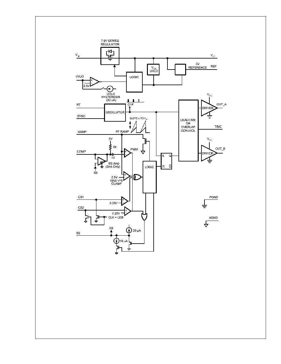
Block Diagram
Simplified Block Diagram
20086902
LM5025
www.national.com
4
Absolute Maximum Ratings
(Note 1)
If Military/Aerospace specified devices are required,
please contact the National Semiconductor Sales Office/
Distributors for availability and specifications.
V
IN
to GND
-0.3V to 100V
V
CC
to GND
-0.3V to 16V
CS1, CS2 to GND
-0.3 to 1.00V
All other inputs to GND
-0.3 to 7V
ESD Rating (Note 2)
Human Body Model
2kV
Machine Model
200V
Storage Temperature Range
-55�C to 150�C
Junction Temperature
150�C
Operating Ratings
(Note 1)
V
IN
Voltage
13 to 90V
External Voltage Applied to V
CC
8 to 15V
Operating Junction Temperature
-40�C to +125�C
Electrical Characteristics
Specifications with standard typeface are for T
J
= 25�C, and those with boldface type apply over full Operating Junction
Temperature range. V
IN
= 48V, V
CC
= 10V, RT = 31.3k
, R
SET
= 27.4k
) unless otherwise stated (Note 3)
Symbol
Parameter
Conditions
Min
Typ
Max
Units
Startup Regulator
V
CC
Reg
V
CC
Regulation
No Load
7.3
7.6
7.9
V
V
CC
Current Limit
(Note 4)
20
25
mA
I-V
IN
Startup Regulator
Leakage (external Vcc
Supply)
V
IN
= 100V
165
500
�A
Shutdown Current (Iin)
UVLO = 0V
350
450
�A
V
CC
Supply
V
CC
Under-voltage
Lockout Voltage
(positive going V
cc
)
V
CC
Reg
- 220mV
V
CC
Reg -
120mV
V
V
CC
Under-voltage
Hysteresis
1.0
1.5
2.0
V
V
CC
Supply Current
(I
CC
)
C
gate
= 0
4.2
mA
Reference Supply
V
REF
Ref Voltage
I
REF
= 0 mA
4.85
5
5.15
V
Ref Voltage
Regulation
I
REF
= 0 to 10mA
25
50
mV
Ref Current Limit
10
20
mA
Current Limit
CS1 Prop
CS1 Delay to Output
CS1 Step from 0 to 0.4V
Time to onset of OUT
Transition (90%)
C
gate
= 0
40
ns
CS2 Prop
CS2 Delay to Output
CS2 Step from 0 to 0.4V
Time to onset of OUT
Transition (90%)
C
gate
= 0
50
ns
Cycle by Cycle
Threshold Voltage
(CS1)
0.22
0.25
0.28
V
Cycle Skip Threshold
Voltage (CS2)
Resets SS capacitor;
auto restart
0.22
0.25
0.28
V
Leading Edge
Blanking Time
50
ns
CS Sink Impedance
(clocked)
I
CS
= 10mA
30
50
LM5025
www.national.com
5