 | –≠–ª–µ–∫—Ç—Ä–æ–Ω–Ω—ã–π –∫–æ–º–ø–æ–Ω–µ–Ω—Ç: LM5026SD | –°–∫–∞—á–∞—Ç—å:  PDF PDF  ZIP ZIP |

LM5026
Active Clamp Current Mode PWM Controller
General Description
The LM5026 PWM controller contains all of the features
necessary to implement power converters utilizing the active
clamp / reset technique with current mode control. With the
active clamp technique, higher efficiencies and greater
power densities can be realized compared to conventional
catch winding or RDC clamp / reset techniques. Two control
outputs are provided, the main power switch control
(OUT_A) and the active clamp switch control (OUT_B). The
device can be configured to control either a P-Channel or
N-Channel clamp switch. The main gate driver features a
compound
configuration,
consisting
of
both
MOS
and Bipolar devices, providing superior gate drive character-
istics. The LM5026 can be configured to operate with bias
voltages over a wide input range of 8V to 100V. Additional
features include programmable maximum duty cycle, line
under-voltage lockout, cycle-by-cycle current limit, hiccup
mode fault operation with adjustable timeout delay, PWM
slope compensation, soft-start, 1MHz capable oscillator with
synchronization input / output capability, precision reference
and thermal shutdown.
Features
n
Current Mode Control
n
Internal 100V Start-up Bias Regulator
n
3A Compound Main Gate Driver
n
High Bandwidth Opto-coupler Interface
n
Programmable Line Under-Voltage Lockout (UVLO) with
Adjustable Hysteresis
n
Versatile Dual Mode Over-Current Protection with hiccup
delay timer
n
Programmable Overlap or Deadtime between the Main
and Active Clamp Outputs
n
Programmable Maximum Duty Cycle Clamp
n
Programmable Soft-start
n
Leading Edge Blanking
n
Resistor Programmed 1MHz Capable Oscillator
n
Oscillator Sync I/O Capability
n
Precision 5V Reference
Packages
n
TSSOP-16
n
LLP-16 (5x5 mm) Thermally Enhanced (Available
Soon)
Typical Application Circuit
20147901
Simplified Forward Power Converter with Active Clamp Reset
August 2005
LM5026
Active
Clamp
Current
Mode
PWM
Controller
© 2005 National Semiconductor Corporation
DS201479
www.national.com
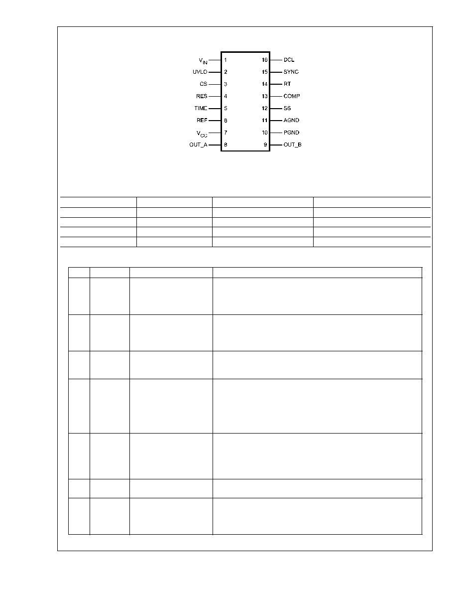
Connection Diagram
20147902
16-Lead TSSOP, LLP
Ordering Information
Order Number
Package Type
NSC Package Drawing
Supplied As
LM5026MT
TSSOP-16
MTC16
92 Units per anti-static tube
LM5026MTX
TSSOP-16
MTC16
2500 Units on Tape and Reel
LM5026SD
LLP-16
SDA16A
Available Soon
LM5026SDX
LLP-16
SDA16A
Available Soon
Pin Descriptions
PIN
NAME
DESCRIPTION
APPLICATION INFORMATION
1
VIN
Input Voltage Source
Input to the Start-up Regulator. Operating input range is 13V to 100V
with transient capability to 105V. For power sources outside of this
range, the LM5026 can be biased directly at VCC by an external
regulator.
2
UVLO
Line Under-Voltage Lockout An external voltage divider from the power source sets the shutdown
and standby comparator levels. When UVLO reaches the 0.4V threshold
the VCC and REF regulators are enabled. At the 1.25V threshold the SS
pin is released and the device enters the active mode.
3
CS
Current Sense input for
current mode control and
current limit
If CS exceeds 0.5V the output pulse will be terminated, entering
cycle-by-cycle current limit. An internal switch holds CS low for 100nS
after OUT_A switches high to blank leading edge transients.
4
RES
Restart Timer
If cycle-by-cycle current limit is reached during any cycle, a 10uA current
is sourced to the RES pin capacitor. If the RES capacitor voltage
reaches 2.5V, the soft-start capacitor will be fully discharged and then
released with a pull-up current of 1uA. After the first output pulse at
OUT_A (when SS =1.4V), the SS pin charging current will revert back to
50 µA.
5
TIME
Gate Drive Overlap or
Deadtime Control
An external resistor (RSET) sets either the overlap time or deadtime for
the active clamp output. An RSET resistor connected between TIME and
AGND produces in-phase OUT_A and OUT_B pulses with overlap. An
RSET resistor connected between TIME and REF produces out-of-phase
OUT_A and OUT_B pulses with deadtime.
6
REF
Output of 5V Reference
Maximum output current is 10mA. Locally decouple with a 0.1µF
capacitor.
7
VCC
Output of the high voltage
start-up regulator. The VCC
voltage is regulated to 7.6
V.
If an auxiliary winding raises the voltage on this pin above the regulation
setpoint, the internal start-up regulator will shutdown, thus reducing the
IC power dissipation.
LM5026
www.national.com
2
Pin Descriptions
(Continued)
PIN
NAME
DESCRIPTION
APPLICATION INFORMATION
8
OUT_A
Main Output Driver
Output of the main switch PWM gate driver. Capable of 3A peak sink
current.
9
OUT_B
Active Clamp Output Driver
Output of the active clamp switch gate driver. Capable of 0.5A peak
source and sink current.
10
PGND
Power Ground
Connect directly to Analog Ground
11
AGND
Analog Return
Connect directly to Power Ground.
12
SS
Soft-start
An external capacitor and an internal 50 µA current source set the
soft-start ramp. The SS current source is reduced to 1 µA following a
restart event. The soft-stop discharge current is 50 µA.
13
COMP
Input to the Pulse Width
Modulator
The external opto-coupler connected to the COMP pin sources current
into an internal NPN current mirror. The PWM duty cycle is maximum
with zero input current, while 1mA reduces the duty cycle to zero. The
current mirror improves the frequency response by reducing the ac
voltage across the opto-coupler detector.
14
RT
Oscillator Frequency
Control
Normally biased at 2V. The total external resistance connected between
RT and AGND sets the internal oscillator frequency.
15
SYNC
Oscillator Synchronization
Input/Output
The internal oscillator can be synchronized to an external clock with an
external pull-down device. Multiple LM5026 devices can be synchronized
together by connection of their SYNC pins.
16
DCL
Maximum Duty Cycle
Control
An external resistor divider connected from RT to AGND sets the
maximum output duty cycle for OUT_A.
-
Exposed
Pad (LLP
Package
Only)
Exposed Pad, underside of
LLP package
Connect to system ground plane for reduced thermal resistance.
LM5026
www.national.com
3
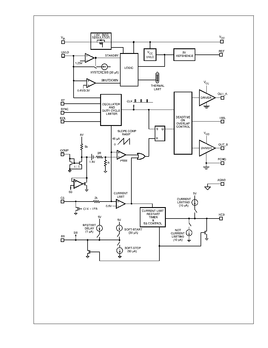
Block Diagram
20147912
FIGURE 1. Simplified Block Diagram
LM5026
www.national.com
4
Absolute Maximum Ratings
(Note 1)
If Military/Aerospace specified devices are required,
please contact the National Semiconductor Sales Office/
Distributors for availability and specifications.
V
IN
to GND
-0.3V to 105V
V
CC
to GND
-0.3V to 16V
CS to GND
-0.3 to 1.0V
COMP Input Current
10mA
All other inputs to GND
-0.3 to 7V
ESD Rating (Note 2)
Human Body Model
2kV
Storage Temperature Range
-65∞C to 150∞C
Junction Temperature
150∞C
Operating Ratings
(Note 1)
V
IN
Voltage
13 to 100V
External Voltage Applied to V
CC
8V to 15V
Operating Junction Temperature
-40∞C to +125∞C
Electrical Characteristics
Specifications with standard typeface are for T
J
= 25∞C, and those with boldface type apply over full Operating Junction
Temperature range. V
IN
= 48V, V
CC
= 10V, RT = 30.0k
, R
SET
= 34.8k
) unless otherwise stated (Note 3)
Symbol
Parameter
Conditions
Min
Typ
Max
Units
Startup Regulator
V
CC
Reg
V
CC
Regulation
No Load
7.3
7.6
7.9
V
V
CC
Current Limit
(Note 4)
20
25
mA
I-V
IN
Startup Regulator
Leakage (external
Vcc Supply)
V
IN
= 100V
165
500
µA
Shutdown Current
(Iin)
UVLO = 0V
350
450
µA
V
CC
Supply
V
CC
Under-voltage
Lockout Voltage
(positive going V
cc
)
V
CC
Reg -
220mV
V
CC
Reg -
120mV
V
V
CC
Under-voltage
Hysteresis
1.0
1.5
2.0
V
V
CC
Supply Current
(I
CC
)
C
gate
= 0, UVLO = 1.3V
4.2
mA
Reference Supply
V
REF
Ref Voltage
I
REF
= 0 mA
4.85
5
5.15
V
Ref Voltage
Regulation
I
REF
= 0 to 10mA
25
50
mV
Ref Current Limit
10
20
mA
UVLO Shutdown/Standby
Undervoltage
Shutdown Threshold
0.3
0.4
0.5
V
Undervoltage
Shutdown Hysteresis
0.1
V
Undervoltage
Standby Threshold
1.21
1.25
1.29
V
Undervoltage
Standby Hysteresis
Current Source
16
20
24
µA
Current Limit
Cycle by Cycle
Threshold Voltage
0.45
0.5
0.55
V
ILIM Delay to Output
CS step from 0 to 0.6V Time
to onset of OUT transition
(90%) Cgate=0
40
ns
Leading Edge
Blanking Time
70
100
130
ns
LM5026
www.national.com
5

Electrical Characteristics
(Continued)
Specifications with standard typeface are for T
J
= 25∞C, and those with boldface type apply over full Operating Junction
Temperature range. V
IN
= 48V, V
CC
= 10V, RT = 30.0k
, R
SET
= 34.8k
) unless otherwise stated (Note 3)
Symbol
Parameter
Conditions
Min
Typ
Max
Units
CS Sink Impedance
(clocked)
I
CS
= 10mA
30
50
Over Current Restart
Restart Threshold
2.4
2.55
2.7
V
Fault Charging
Current
7.5
10
12.5
µA
Discharging Current
7.5
10
12.5
µA
Soft-Start
Soft-start Current
Source
38
50
58
µA
Soft-stop Current
Sink
38
50
58
Soft-start Current
Source following a
restart event
0.6
1
1.3
Oscillator
Frequency1
RT = 30.0 k
180
200
220
kHz
Frequency2
RT = 10.0 k
520
590
660
kHz
SYNC Source
Current
200
µA
SYNC Sink
Impedance
Can sync up to 5 like
controllers minimum
100
Sync Threshold
(falling)
1.4
V
Sync Pulse Width
Minimum
15
ns
PWM Comparator
Delay to Output
CS stepped, Time to onset of
OUT_A transition low
40
ns
Mimimum Duty
Cycle
I
COMP
= 1mA
0
%
Maximum Duty
Cycle Limit 1
UVLO=1.3V, COMP = open,
V
DCL
= 2.5V
80
%
Maximum Duty
Cycle Limit 2
UVLO=1.3V, COMP = open,
V
DCL
= V
RT
x 0.875
70
%
Maximum Duty
Cycle Limit 3
UVLO=2.92V, COMP = open,
V
DCL
= 2.5V
40
%
SS to PWM Offset
1.4
V
COMP Input
Impedance
Small signal impedance
1700
Slope Compensation
Amplitude
Delta increase at PWM
comparator to CS
75
90
115
mV
Output Section
OUT_A High
Saturation
MOS Device
@
Iout = -10mA,
5
10
OUTPUT_A Peak
Current Sink
Bipolar Device
@
Vcc/2
3
A
OUT_A Low
Saturation
MOS Device
@
Iout = 10mA,
6
9
LM5026
www.national.com
6
Electrical Characteristics
(Continued)
Specifications with standard typeface are for T
J
= 25∞C, and those with boldface type apply over full Operating Junction
Temperature range. V
IN
= 48V, V
CC
= 10V, RT = 30.0k
, R
SET
= 34.8k
) unless otherwise stated (Note 3)
Symbol
Parameter
Conditions
Min
Typ
Max
Units
OUTPUT_A Rise
Time
C
gate
= 2.2nF
20
ns
OUTPUT_A Fall
Time
C
gate
= 2.2nF
15
ns
OUT_B High
Saturation
Iout = -10mA,
10
20
OUT_B Low
Saturation
Iout = 10mA,
10
20
OUTPUT_B Rise
Time
C
gate
= 470pF
15
ns
OUTPUT_B Fall
Time
C
gate
= 470pF
15
ns
Output Timing Control
Overlap Time
R
SET
= 34.8 k
connected to
GND, 50% to 50% transitions
70
100
130
ns
Deadtime
R
SET
= 30.0 k
connected to
REF, 50% to 50% transitions
70
100
130
ns
Thermal Shutdown
T
SD
Thermal Shutdown
Temp.
150
165
∞C
Thermal Shutdown
Hysteresis
25
∞C
Thermal Resistance
JA
Junction to Ambient
MTC Package
125
∞C/W
SDA Package
32
∞C/W
Note 1: Absolute Maximum Ratings are limits beyond which damage to the device may occur. Operating Ratings are conditions under which operation of the device
is intended to be functional. For guaranteed specifications and test conditions, see the Electrical Characteristics.
Note 2: The human body model is a 100 pF capacitor discharged through a 1.5 k
resistor into each pin.
Note 3: Min and Max limits are 100% production tested at 25
o
C. Limits over the operating temperature range are guaranteed through correlation using Statistical
Quality Control (SQC) methods. Limits are used to calculate National's Average Outgoing Quality Level (AOQL).
Note 4: Device thermal limitations may limit usable range.
LM5026
www.national.com
7
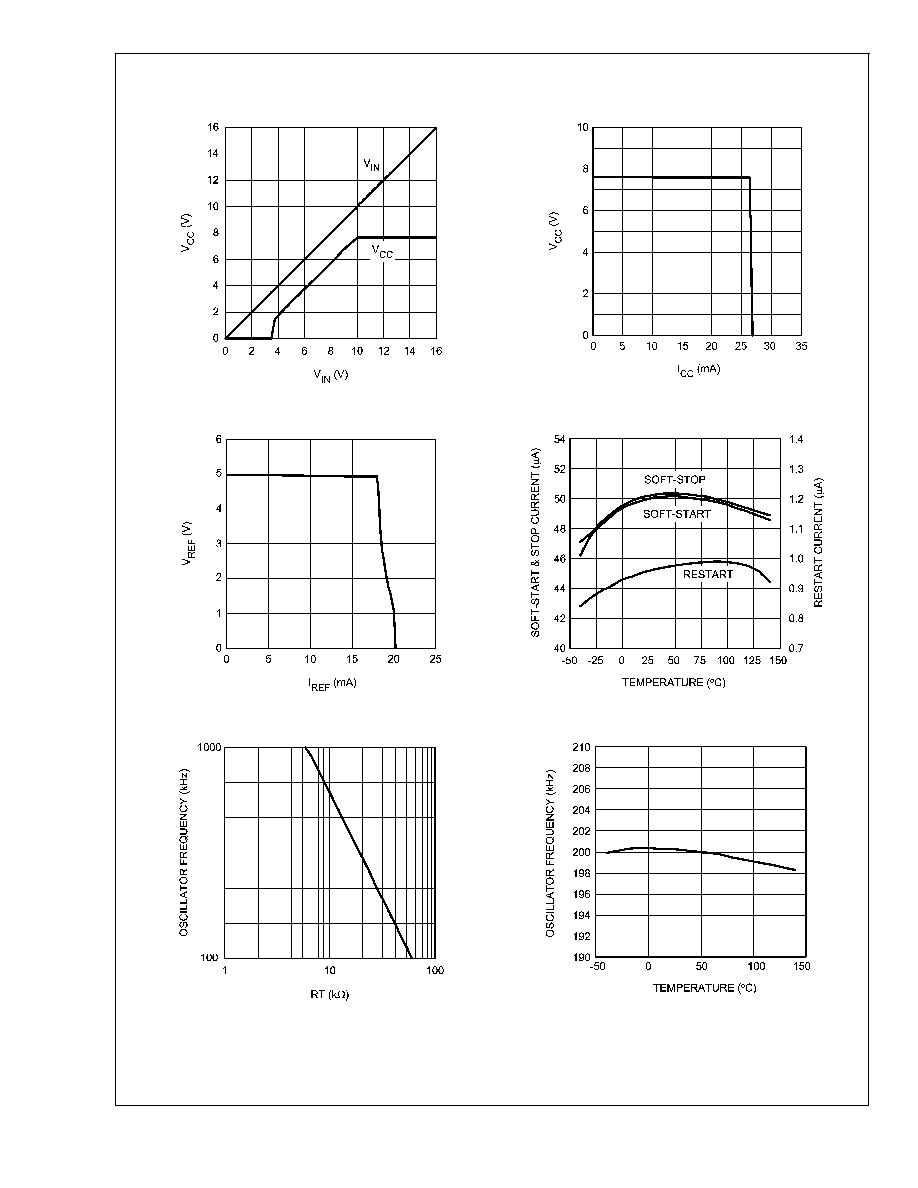
Typical Performance Characteristics
V
CC
Regulator Start-up Characteristics, V
CC
vs Vin
V
CC
vs I
CC
20147903
20147904
V
REF
vs I
REF
Soft-start, Soft-stop and Restart Current vs Temperature
20147905
20147938
Oscillator Frequency vs RT
Oscillator Frequency vs Temperature
20147906
20147907
LM5026
www.national.com
8

Typical Performance Characteristics
(Continued)
Overlap Time vs R
SET
Overlap Time vs Temperature
20147908
20147909
Deadtime vs R
SET
Deadtime vs Temperature
20147910
20147911
Max Duty Cycle vs UVLO
Max Duty Cycle vs DCL
20147935
20147936
LM5026
www.national.com
9
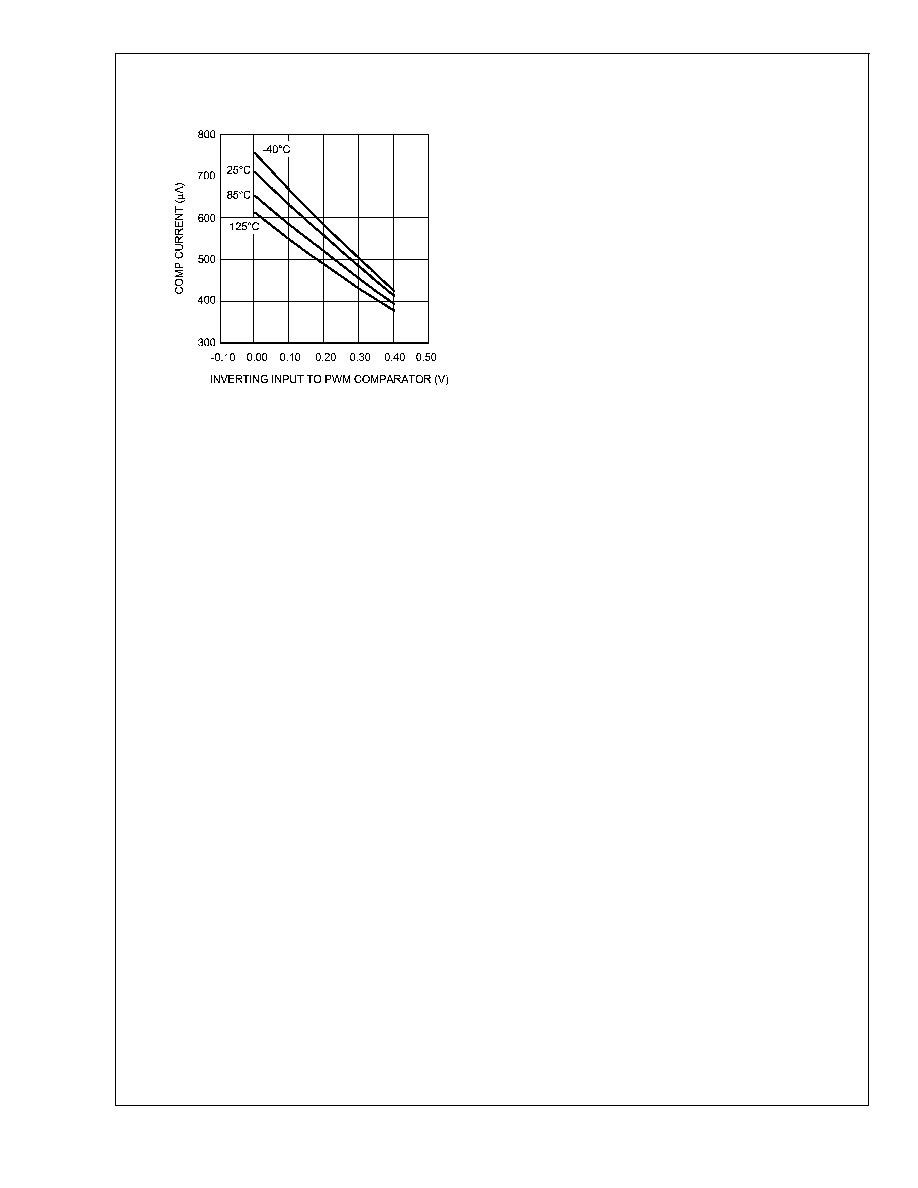
Typical Performance Characteristics
(Continued)
COMP Current vs INV PWM Comparator Voltage
20147937
LM5026
www.national.com
10

Detailed Operating Description
The LM5026 PWM controller contains all of the features
necessary to implement power converters utilizing the active
clamp reset technique with current mode control. With the
active clamp reset, higher efficiencies and greater power
densities can be realized compared to conventional catch
winding or RDC clamp reset techniques. The LM5026 pro-
vides two control outputs, the main power switch control
(OUT_A) and the active clamp switch control (OUT_B). The
device can be configured to drive either a P-Channel or
N-Channel clamp switch. The main switch gate driver fea-
tures a compound configuration consisting of both MOS and
bipolar devices, which provide superior gate drive character-
istics. The LM5026 can be configured to operate with bias
voltages over a wide input range from 8V to 100V. Additional
features include programmable maximum duty cycle, line
under-voltage lockout, cycle-by-cycle current limit, hiccup
mode fault protection with adjustable delays, PWM slope
compensation, soft-start, a 1MHz capable oscillator with syn-
chronization Input / Output capability, precision reference
and thermal shutdown.
High Voltage Start-Up Regulator
The LM5026 contains an internal high voltage start-up regu-
lator that allows the input pin (VIN) to be connected directly
to a nominal 48V dc line voltage. The regulator output (VCC)
is internally current limited to 20mA. When power is applied
and the UVLO pin potential is greater than 0.4V, the regula-
tor is enabled and sources current into an external capacitor
connected to the VCC pin. The recommended capacitance
range for the VCC regulator is 0.1µF to 100µF. The VCC
regulator provides power to the internal voltage reference,
PWM controller and gate drivers. The controller outputs are
enabled when the voltage on the VCC pin reaches the
regulation point of 7.6V, the internal voltage reference (REF)
reaches its regulation point of 5V and the UVLO voltage is
greater than 1.25V. In typical applications, an auxiliary trans-
former winding is connected through a diode to the VCC pin.
This winding must raise the VCC voltage above 8V to shut
off the internal start-up regulator. Powering VCC from an
auxiliary winding improves efficiency while reducing the con-
troller's power dissipation.
The external VCC capacitor must be sized such that the
current delivered from the capacitor and the VCC regulator
will maintain a VCC voltage greater than 6.2V during the
initial start-up. During a fault mode when the converter aux-
iliary winding is inactive, external current draw on the VCC
line should be limited such that the power dissipated in the
start-up regulator does not exceed the maximum power
dissipation of the IC package. An external start-up or bias
regulator can be used to power the LM5026 instead of the
internal start-up regulator by connecting the VCC and the
VIN pins together and connecting an external bias supply to
these two pins.
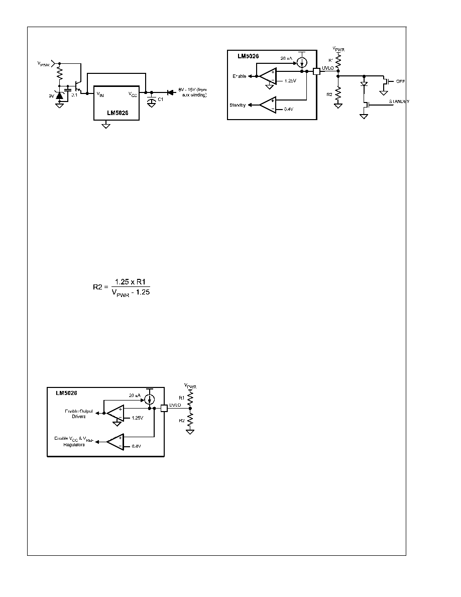
Line Under-Voltage Detector
The LM5026 contains a dual level Under-Voltage Lockout
(UVLO) circuit. When the UVLO pin voltage is below 0.4V
the controller is in a low current shutdown mode. When the
UVLO pin voltage is greater than 0.4V but less than 1.25V,
the controller is in standby mode. In standby mode the VCC
and REF bias regulators are active while the controller out-
puts are disabled. When the VCC and REF outputs exceed
the VCC and REF under-voltage thresholds and the UVLO
pin voltage is greater than 1.25V, the outputs are enabled
and normal operation begins. An external set-point voltage
divider from VIN to GND can be used to set the operational
range of the converter. The divider must be designed such
that the voltage at the UVLO pin will be greater than 1.25V
when VIN is in the desired operating range. UVLO hysteresis
is accomplished with an internal 20uA current source that is
switched on or off into the impedance of the set-point divider.
When the UVLO threshold is exceeded, the current source is
activated to instantly raise the voltage at the UVLO pin.
When the UVLO pin voltage falls below the 1.25V threshold,
the current source is turned off causing the voltage at the
UVLO pin to fall. The hysteresis of the 0.4V shutdown com-
parator is fixed at 100mV.
The UVLO pin can also be used to implement various re-
mote enable / disable functions. Pulling the UVLO pin below
the 0.4V threshold totally disables the controller. Pulling the
UVLO pin to a potential between 1.25 and 0.4V places the
controller in standby with the VCC and REF regulators op-
erating. Turning off a converter by forcing the UVLO pin to
the standby condition provides a controlled soft-stop. The
controller outputs are not directly disabled in standby mode,
rather the soft-start capacitor is discharged with a 50µA sink
current. Discharging the soft-start capacitor gradually re-
duces the PWM duty cycle to zero, providing a slow con-
trolled discharge of the power converter output filter. This
controlled discharge can help prevent uncontrolled behavior
of self-driven synchronous rectifiers during turn-off.
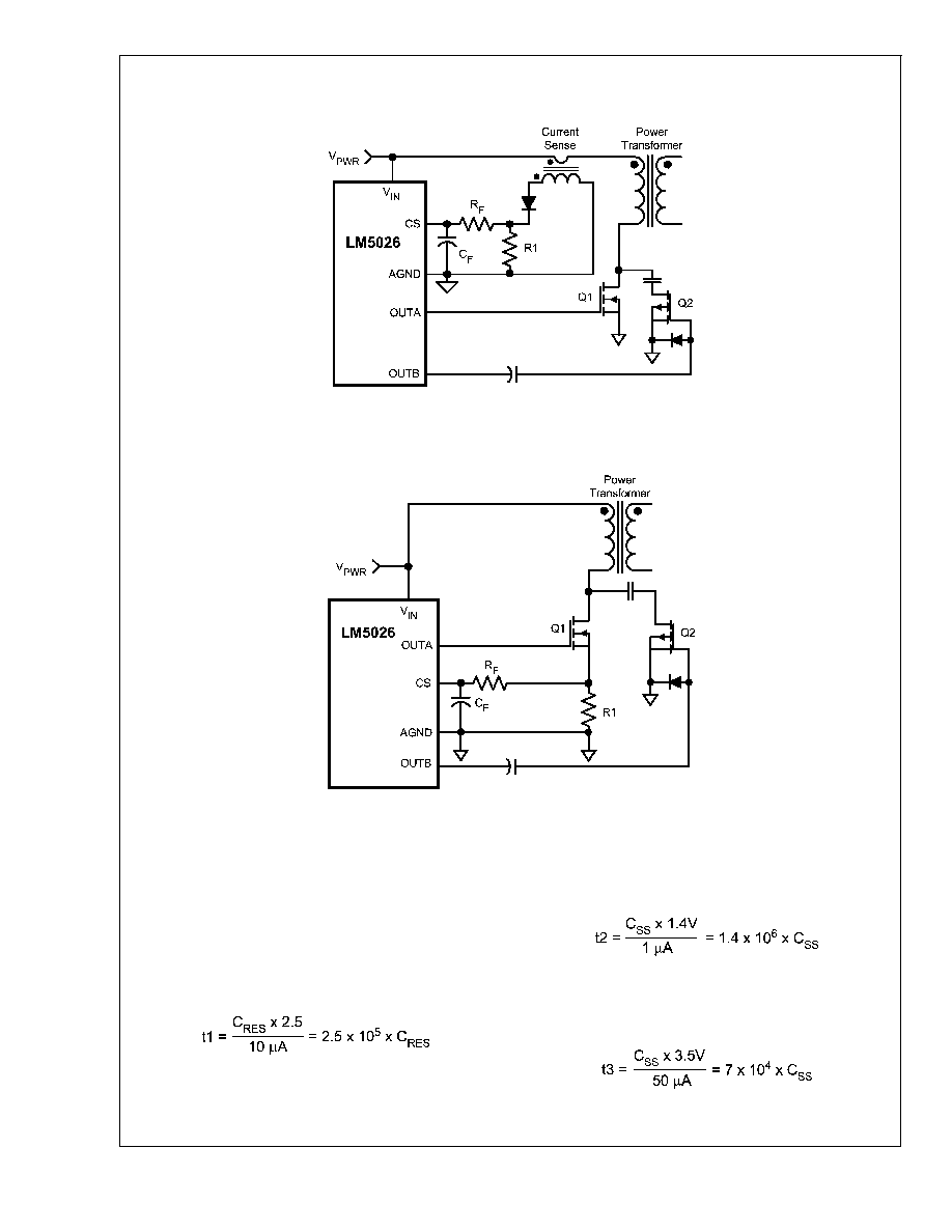
PWM Outputs
The relative phase of the main switch gate driver OUT_A and
active clamp gate driver OUT_B can be configured for mul-
tiple applications. For active clamp configurations utilizing a
ground referenced P-Channel clamp switch, the two outputs
should be in phase, with the active clamp output overlapping
the main output. For active clamp configurations utilizing a
high side N-Channel switch, the active clamp output should
be out of phase with main output and there should be a dead
time between the two gate drive pulses. A distinguishing
feature of the LM5026 is the ability to accurately configure
either deadtime (both off) or overlap time (both on) of the
gate driver outputs. The overlap / deadtime magnitude is
controlled by the resistor value (RSET) connected to the
TIME pin of the controller. The opposite end of the resistor
can be connected to either REF for deadtime control or to
AGND for overlap control. The internal configuration detector
senses the direction of current flow in the TIME pin resistor
and configures the phase relationship of the main and active
clamp outputs.
LM5026
www.national.com
11
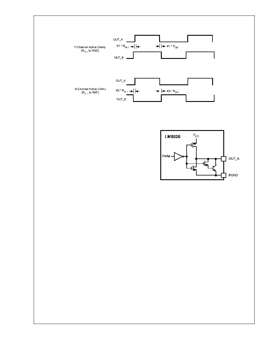
PWM Outputs
(Continued)
The rising edge overlap or deadtime and the falling edge
overlap or deadtime are identical and are independent of
operating frequency or duty cycle. The magnitude of the
overlap/deadtime can be calculated as follows:
Overlap Time = 2.8 x R
SET
+ 2
Deadtime = 2.9 x R
SET
+ 14
With R
SET
in K Ohms and overlap / deadtime in nanosec-
onds
Gate Driver Outputs
The LM5026 provides two gate driver outputs, the main
power switch control (OUT_A) and the active clamp switch
control (OUT_B). The main gate driver features a compound
configuration, consisting of both MOS and bipolar devices,
which provide superior gate drive characteristics. The bipolar
device provides most of the drive current capability and sinks
a relatively constant current, which is ideal for driving large
power MOSFETs. As the switching event nears conclusion
and the bipolar device saturates, the internal MOS device
provides a low impedance to compete the switching event.
During turn-off at the Miller plateau region, typically between
2V - 4V, the voltage differential between the output and
PGND is small and the current source characteristic of the
bipolar device is beneficial to reduce the transition time.
During turn-on, the resistive characteristics of a purely MOS
gate driver is adequate since the supply to output voltage
differential is fairly large in the Miller region.
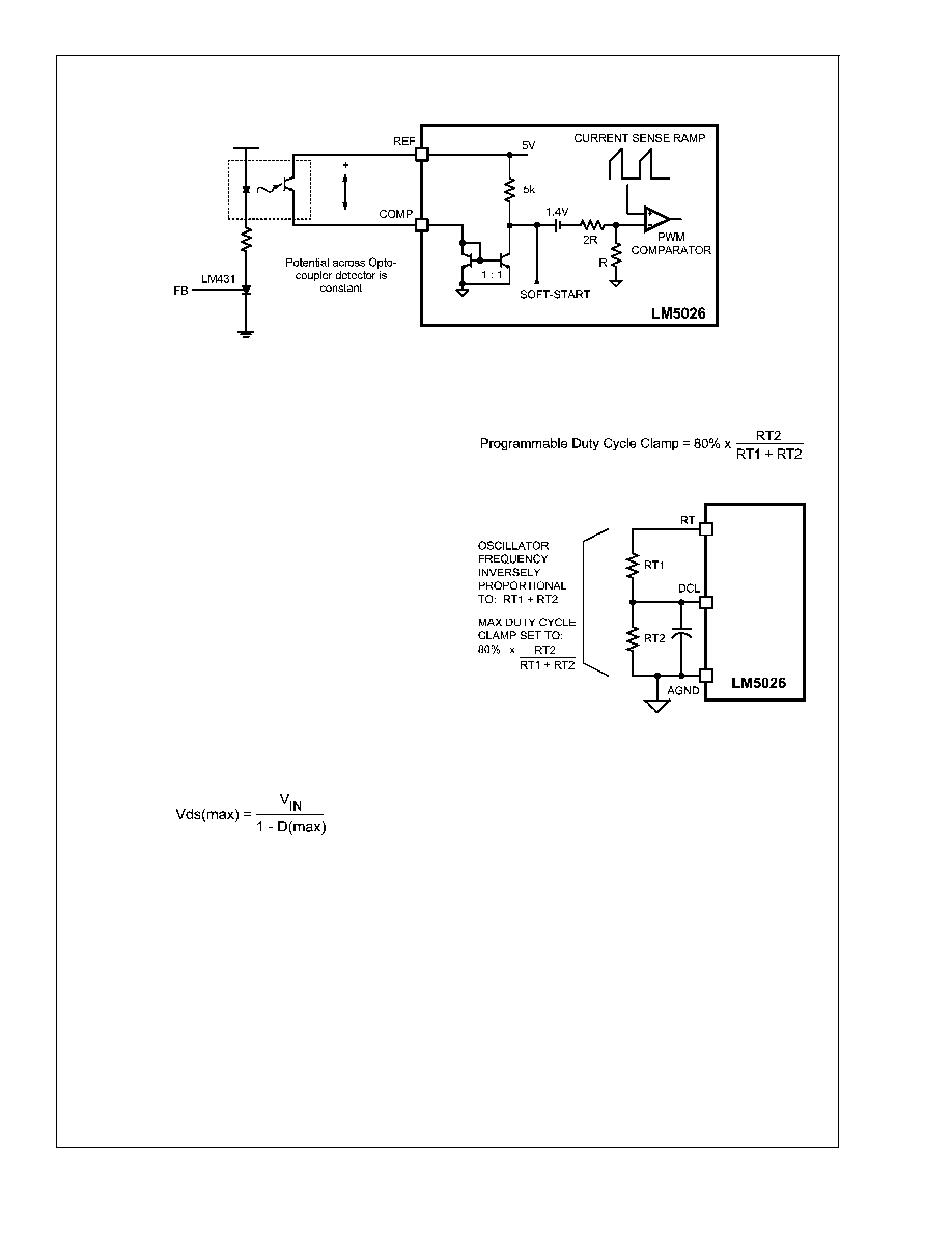
PWM Comparator/Slope
Compensation
The PWM comparator modulates the pulse width of the
controller output by comparing the current sense ramp signal
to the loop error signal. This comparator is optimized for
speed in order to achieve minimum controllable duty cycles.
The loop error signal is input into the controller in the form of
a control current into the COMP pin. The COMP pin control
current is internally mirrored by a matched pair of NPN
transistors which sink current through a 5 k
resistor con-
nected to the 5V reference. The resulting error signal passes
through a 1.4V level shift and a gain reducing 3:1 resistor
divider before being applied to the pulse width modulator.
The opto-coupler detector can be connected between the
REF pin and the COMP pin. Because the COMP pin is
controlled by a current input, the potential difference across
the optocoupler detector is nearly constant. The bandwidth
limiting phase delay which is normally introduced by the
significant capacitance of the opto-coupler is greatly re-
duced. Greater system loop bandwidth can be realized,
since the bandwidth-limiting pole associated with the opto-
coupler is now at a much higher frequency. The PWM com-
parator polarity is configured such that with no current into
the COMP pin, the controller produces the maximum duty
cycle at the main gate driver output.
20147913
FIGURE 2. PWM Output Phasing / Timing
20147914
FIGURE 3. Compound Gate Driver
LM5026
www.national.com
12
PWM Comparator/Slope Compensation
(Continued)
For duty cycles greater than 50 percent, current mode con-
trol circuits are subject to sub-harmonic oscillation. By add-
ing an additional fixed slope voltage ramp signal (slope
compensation) to the current sense signal, this oscillation
can be avoided. The LM5026 integrates this slope compen-
sation by summing a current ramp generated by the oscilla-
tor with the current sense signal. The PWM comparator
ramp signal is a combination of the current waveform at the
CS pin, and an internally generated slope compensation
ramp derived from the oscillator. The internal ramp has an
amplitude of 0 to 45 µA which is sourced into an internal 2 k
resistor, plus the external impedance at the CS pin. Addi-
tional slope compensation may be added by increasing the
source impedance of the current sense signal.
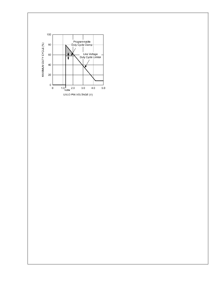
Maximum Duty Cycle Clamp
Controlling the maximum duty cycle of an active clamp reset
PWM controller is necessary to limit the voltage stress on the
main and active clamp MOSFETs. The relationship between
the maximum drain-source voltage of the MOSFETs and the
maximum PWM duty cycle is provided by the following equa-
tion:
The main output (OUT_A) duty cycle is normally controlled
by the control current sourced into the COMP pin from the
external feedback circuit. When the feedback demands
maximum output from the converter, the duty cycle will be
limited by one of two circuits within the LM5026: the user
programmable duty cycle clamp and the voltage-dependent
duty cycle limiter, which varies inversely with the input line
voltage.
Programmable Duty Cycle Clamp ≠ The maximum allowed
duty cycle can be programmed by setting a voltage at the
DCL pin to a value less than 2V. The recommended method
to set the DCL pin voltage is with a resistor divider connected
from the RT pin to AGND. The voltage at the RT pin is
internally regulated to 2V, while the current sourced from the
RT pin sets the oscillator frequency. The maximum duty can
be programmed, according to the following equation:
Line Voltage Duty Cycle Limiter - The maximum duty cycle
for the main output driver is also limited by the voltage at the
UVLO pin, which is normally proportional to VIN. The con-
troller outputs are disabled until the UVLO pin voltage ex-
ceeds 1.25V. At the minimum operating voltage (when UVLO
= 1.25V) the maximum duty cycle starts at the duty cycle
clamp level programmed by the DCL pin voltage (80% or
less). As the line voltage increases, the maximum duty cycle
decreases linearly with increasing UVLO voltage, as illus-
trated in Figure 6. Ultimately the duty cycle of the main
output is controlled to the least of the following three vari-
ables: the duty cycle controlled by the PWM comparator, the
programmable maximum duty cycle clamp, or the line volt-
age dependent duty cycle limiter.
20147915
FIGURE 4. Opto-coupler to LM5026 COMP Interface
20147916
FIGURE 5. Programming oscillator Frequency and
Maximum Duty Cycle Clamp
LM5026
www.national.com
13
Maximum Duty Cycle Clamp
(Continued)
Soft-Start/Soft-Stop
The soft-start circuit allows the regulator to gradually reach a
steady state operating point, thereby reducing start-up
stresses and current surges. Upon turn-on, the SS pin ca-
pacitor is discharged by an internal switch. When the UVLO,
VCC and REF pins reach their operating thresholds, the SS
capacitor is released and charged with a 50uA current
source. The PWM comparator control voltage is clamped to
the SS pin voltage. When the PWM input reaches 1.4V,
output pulses commence with slowly increasing duty cycle.
The voltage at the SS pin eventually increases to 5V, while
the voltage at the PWM comparator increases to the value
required for regulation determined by the voltage feedback
loop.
If the UVLO pin voltage falls below the 1.25V standby thresh-
old but above the 0.4V shutdown threshold, the 50uA SS pin
source current is disabled and a 50uA sink current dis-
charges the soft-start capacitor. As the SS voltage falls and
clamps the PWM comparator input, the PWM duty cycle will
gradually fall to zero. This soft-stop feature produces a
gradual reduction of the power converter output voltage. This
gradual discharge of the output filter prevents oscillations in
the self-driven synchronous rectifiers on the secondary side
of the converter during turn-off.
Current Sense/Current Limit
The CS input provides a control ramp for the pulse width
modulator and current limit detection for overload protection.
If the sensed voltage at the CS comparator exceeds 0.5V the
present cycle is terminated (cycle-by-cycle current limit
mode).
A small RC filter, located near the controller, is recom-
mended for the CS input pin. An internal FET connected to
the CS input discharges the current sense filter capacitor at
the conclusion of every cycle to improve dynamic perfor-
mance. This same FET remains on for an additional 100nS
at the start of each main switch cycle to attenuate the leading
edge spike in the current sense signal.
The CS comparator is very fast and may respond to short
duration noise pulses. Layout considerations are critical for
the current sense filter and sense resistor. The capacitor
associated with the CS filter must be placed very close to the
device and connected directly to the pins of the LM5026 (CS
and AGND pins). If a current sense transformer is used, both
leads of the transformer secondary should be routed to the
filter network, which should be located close to the IC. If a
sense resistor located in the source of the main switch
MOSFET is used for current sensing, a low inductance type
of resistor is required. When designing with a current sense
resistor, all of the noise sensitive low power ground connec-
tions should be connected together near the AGND pin and
a single connection should be made to the power ground
(sense resistor ground point).
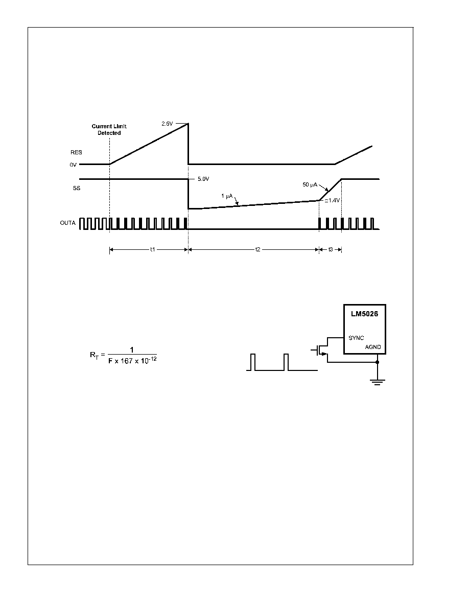
Overload Protection Timer
The LM5026 provides a current limit restart timer to disable
the outputs and force a delayed restart (hiccup mode) if a
current limit condition is repeatedly sensed. The number of
cycle-by-cycle current limit events required to trigger the
restart is programmable by means of an external capacitor at
the RES pin. During each PWM cycle the LM5026 either
sources or sinks current from the RES pin capacitor. If no
current limit is detected during a cycle, a 10uA discharge
current sink is enabled to hold the RES pin at ground. If a
current limit is detected, the 10uA sink current is disabled
and a 10 uA current source causes the voltage at RES pin to
gradually increase. In the event of an extended overload
condition, the LM5026 protects the converter with cycle-by-
cycle current limiting while the voltage at RES pin increases.
If the RES voltage reaches the 2.5V threshold, the following
restart sequence occurs (see Figure 7):
∑
The RES capacitor and SS capacitors are fully dis-
charged.
∑
The soft-start current source is reduced from 50 µA to 1
µA
∑
The SS capacitor voltage slowly increases. When the SS
voltage reaches 1.4V, the PWM comparator will produce
the first output pulse. After the first pulse occurs, the SS
source current reverts to the normal 50 µA level. The SS
voltage increases at its normal rate gradually increasing
the duty cycle of the output drivers
∑
If the overload condition persists after restart, cycle-by-
cycle current limiting will cause the voltage on the RES
capacitor to increase again, repeating the hiccup mode
sequence.
∑
If the overload condition no longer exists after restart, the
RES pin will be held at ground by the 10 µA current sink
and normal operation resumes.
The overload timer function is very versatile and can be
configured for the following modes of protection:
1.
Cycle-by-cycle only: The hiccup mode can be com-
pletely disabled by connecting the RES pin to AGND. In
this configuration, the cycle-by-cycle protection will limit
the output current indefinitely and no hiccup sequences
will occur.
2.
Hiccup only: The timer can be configured for immediate
activation of a hiccup sequence upon detection of an
overload by leaving the RES pin open circuit.
20147917
FIGURE 6. Maximum Duty Cycle vs UVLO Voltage
LM5026
www.national.com
14
Overload Protection Timer
(Continued)
3.
Delayed Hiccup: The most common configuration as
previously described, is a programmed interval of cycle-
by-cycle limiting before initiating a hiccup mode restart.
The advantage of this configuration is short term over-
load conditions will not cause a hiccup mode restart,
however during extended overload conditions the aver-
age dissipation of the power converter will be very low.
4.
Externally Controlled Hiccup: The RES pin can also
be used as an input. By externally driving the pin to a
level greater than the 2.5V hiccup threshold, the control-
ler will be forced into the delayed restart sequence. If the
RES pin is used as an input, the driving source should
be current limited to less than 5 mA. For example, the
external trigger for a delayed restart sequence could
come an over-temperature protection circuit.
Oscillator and Sync Capability
The LM5026 oscillator frequency is set by the external resis-
tance connected between the RT pin and ground (AGND).
To set a desired oscillator frequency (F) the necessary value
of total R
T
resistance can be calculated from:
The R
T
resistor(s) should be located very close to the device
and connected directly to the pins of the IC (RT and AGND).
The SYNC pin can be used to synchronize the internal
oscillator to an external clock. An open drain output is the
recommended interface between the external clock to the
LM5026 SYNC pin as illustrated in Figure 8. The clock pulse
width must be greater than 15 ns. The external clock fre-
quency must be a higher than the free running frequency set
by the R
T
resistance.
20147918
FIGURE 7. Hiccup Over-Load Restart Timing
20147919
FIGURE 8. Sync from External Clock
LM5026
www.national.com
15
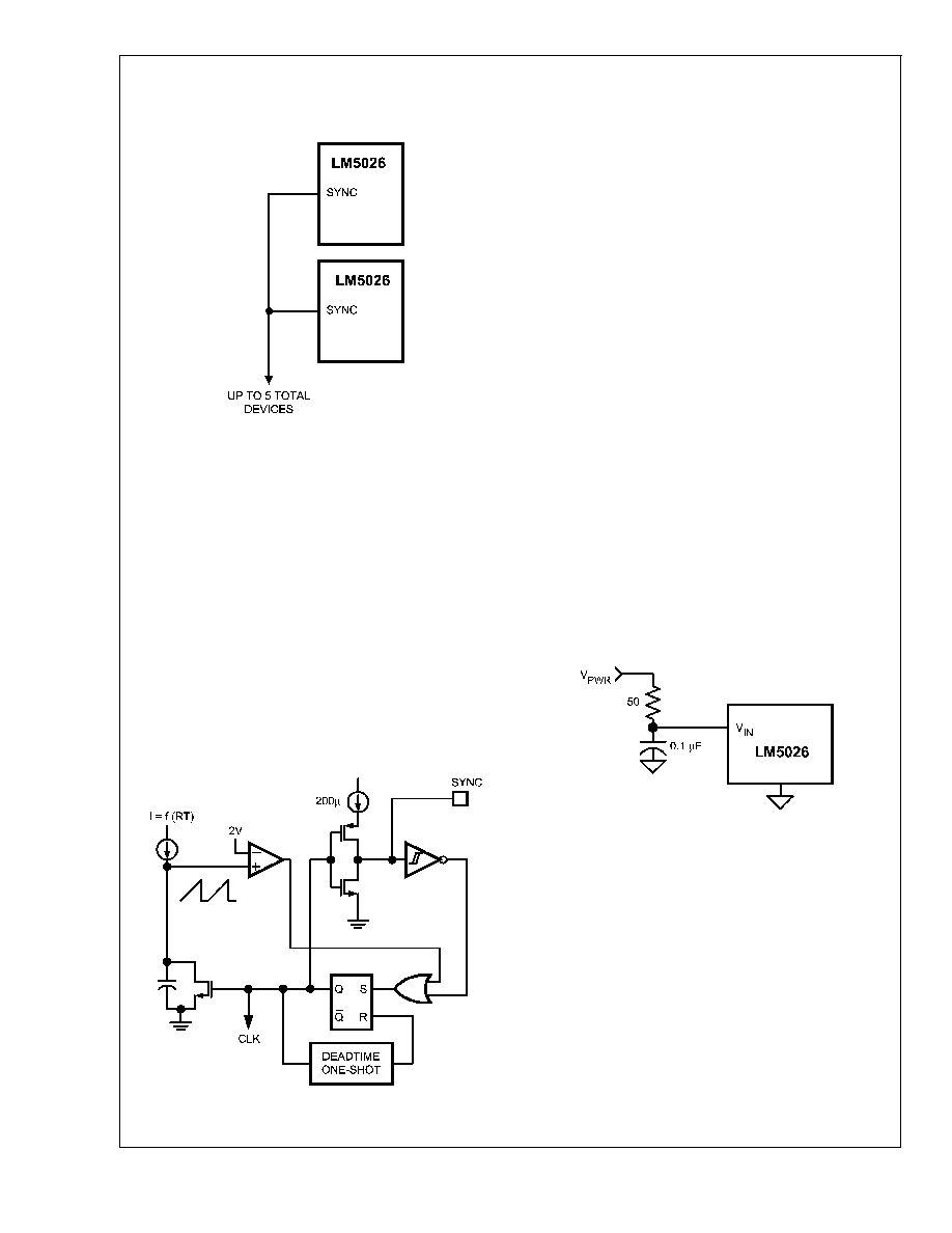
Oscillator and Sync Capability
(Continued)
Multiple LM5026 devices can be synchronized together sim-
ply by connecting the devices SYNC pins together as shown
in Figure 9. Care should be taken to ensure the ground
potential differences between devices are minimized. In this
configuration all of the devices will be synchronized to the
highest frequency device. The internal block diagram of the
oscillator and synchronization circuit is shown in Figure 10.
The SYNC I/O pin is a CMOS buffer with pull-up current
limited to 200 µA. If an external device forces the SYNC pin
low before the internal oscillator ramp completes its charging
cycle, the ramp will be reset and another cycle begins. If the
SYNC pins of multiple LM5026 devices are connected to-
gether, the first SYNC pin that pulls low will reset the oscil-
lator RAMP of all other devices. All controllers will operate in
phase when synchronized using the SYNC I/O feature. Up to
five LM5026 devices can be synchronized using this tech-
nique.
Thermal Protection
Internal Thermal Shutdown circuitry is provided to protect the
integrated circuit in the event the maximum junction tem-
perature is exceeded. When activated, typically at 165∞C,
the controller is forced into a low power standby state with
the output drivers and the bias regulator disabled. The de-
vice will restart after the thermal hysteresis (typically 25∞C).
During thermal shutdown, the soft-start capacitor is fully
discharged and the controller follows a normal start-up se-
quence after the junction temperature falls to the operating
level.
Applications Information
LINE INPUT (VIN)
The LM5026 contains an internal high voltage start-up regu-
lator that allows the input pin (VIN) to be connected directly
to a nominal 48V line voltage. The voltage applied to the VIN
pin can vary in the range of 13 to 100V with transient
capability to 105V. When power is applied and the UVLO pin
potential is greater than 0.4V, the VCC regulator is enabled
and sources current into an external capacitor connected to
the VCC pin. When the voltage on the VCC pin reaches the
regulation point of 7.7V, the internal voltage reference (REF)
is enabled. The reference regulation set point is 5V. The
controller outputs are enabled when the UVLO pin potential
is greater than 1.25V. In typical applications, an auxiliary
transformer winding is connected through a diode to the
VCC pin. This winding must raise the VCC voltage above 8V
to shut off the internal start-up regulator. It is recommended
a filtering circuit shown in Figure 11 be used to suppress
transients, which may occur at the input supply, in particular
when VIN is operated close to the maximum operating rat-
ing.
FOR APPLICATION
>
100V
For applications where the system input voltage exceed
100V or IC power dissipation is a concern, the LM5026 can
be powered from an external start-up regulator as shown in
Figure 12. In this configuration, the VIN and the VCC pins
should be connected together, which allows the LM5026 to
be operated below 13V. The voltage at the VCC pin must be
greater than 8V yet not exceed 15V. An auxiliary winding can
be used to reduce the dissipation in the external regulator
once the power converter is active.
20147920
FIGURE 9. Sync from Multiple Devices
20147921
FIGURE 10. Oscillator Sync I/O Block Diagram
20147922
FIGURE 11. Input Transient Protection
LM5026
www.national.com
16
Applications Information
(Continued)
UNDER-VOLTAGE LOCKOUT (UVLO)
When the UVLO pin voltage is below 0.4V the controller is in
a low current shutdown mode. When the UVLO pin voltage is
greater than 0.4V but less than 1.25V the controller is in
standby mode. When the UVLO pin voltage is greater than
1.25V the controller is fully enabled. Typically, two external
resistors program the minimum operational voltage for the
power converter as shown in Figure 13. When UVLO pin
voltage is above the 1.25V threshold, an internal 20 µA
current source is enabled to raise the voltage at the UVLO
pin, thus providing threshold hysteresis. Resistance values
for R1 and R2 can be determined from:
R1 = V
HYS
/ 20 µA
Where V
PWR
is the desired turn-on voltage and V
HYS
is the
desired UVLO hysteresis at V
PWR
. For example, if the
LM5026 is to be enabled when V
PWR
reaches 33V, and
disabled when V
PWR
is decreased to 30V, R1 calculates to
150 k
, and R2 calculates to 5.9 k. The voltage at the
UVLO pin should not exceed 6V at any time. Be sure to
check both the power and voltage rating for the selected R1
resistor.
Remote configuration of the controller's operational modes
can be accomplished with open drain device(s) connected to
the UVLO pin as shown in Figure 14.
OSCILLATOR (RT, SYNC)
Oscillator (RT, SYNC) The oscillator frequency is generally
selected in conjunction with the design of the system mag-
netic components along with the volume and efficiency goals
for a given power converter design. The total RT resistance
at the RT pin sets the oscillator frequency. The RT resistors
should be one of the first components placed and connected
when designing the PC board. Direct, short connections to
each side of the RT resistors (RT, DCL and AGND pins) are
recommended .
The SYNC pin can be used to synchronize the internal
oscillator to an external clock. An open drain output is the
recommended interface from the external clock to the SYNC
pin. The clock pulse width should be greater than 15 ns. The
external clock must be a higher frequency than the free
running frequency set by the RT resistor. Multiple LM5026
devices can be synchronized together simply by connecting
the devices SYNC pins together. Care should be taken to
ensure the ground potential differences between devices are
minimized. In this configuration all of the devices will be
synchronized to the highest frequency device.
VOLTAGE FEEDBACK (COMP)
The COMP pin is designed to accept the voltage loop feed-
back error signal from the regulated output via an error
amplifier and (typically) an optocoupler. In a typical configu-
ration, VOUT is compared to a precision reference voltage
by the error amplifier. The amplifier's output drives the opto-
coupler, which in turn drives the COMP pin. The parasitic
capacitance of the optocoupler often limits the achievable
loop bandwidth for a given power converter. The optocoupler
LED and detector junction capacitance produce a low fre-
quency pole in the voltage regulation loop. The LM5026
current controlled optocoupler interface (COMP) previously
described, greatly increases the pole frequency associated
with the optocoupler.
CURRENT SENSE (CS)
The CS pin receives an input signal representative of the
transformer primary current, either from a current sense
transformer (Figure 15) or from a resistor in series with the
source of the primary switch (Figure 16). In both cases the
sensed current creates a ramping voltage across R1, while
the R
F
/C
F
filter suppresses noise and transients. R1, R
F
and
C
F
should be as physically close to the LM5026 as possible,
and the ground connection from the current sense trans-
former, or R1, should be a dedicated track to the AGND pin.
The current sense components must provide
>
0.5V at the
CS pin when an over-current condition exists.
20147923
FIGURE 12. Start-up Regulator for V
PWR
>
100V
20147924
FIGURE 13. Basic UVLO Configuration
20147925
FIGURE 14. Remote Standby and Disable Control
LM5026
www.national.com
17
Applications Information
(Continued)
HICCUP MODE CURRENT LIMIT RESTART (RES)
The basic operation of the hiccup mode current limit restart
is described in the functional description. The delay time to
restart is programmed with the selection of the RES pin
capacitor C
RES
as illustrated in Figure 7. In the case of
continuous cycle-by-cycle current limit detection at the CS
pin, the time required for C
RES
to reach the 2.5V hiccup
mode threshold is:
For example, if C
RES
= 0.01 µF the time t1 is approximately
2.5 ms.
The cool down time, t2 is set by the soft-start capacitor (C
SS
)
and the internal 1 µA SS current source, and is equal to:
If C
SS
= 0.01 µF, t2 is
14 ms.
The soft-start time t3 is set by the internal 50 µA current
source, and is equal to:
20147926
FIGURE 15. Current Sense Using a Current Sense Transformer
20147927
FIGURE 16. Current Sense Using a Source Sense Resistor (R1)
LM5026
www.national.com
18
Applications Information
(Continued)
The time t2 provides a periodic cool-down time for the power
converter in the event of a sustained overload or short
circuit. This results in lower average input current and lower
power dissipated within the power components. It is recom-
mended that the ratio of t2/(t1 + t3) be in the range of 5 to 10
to make good use of this feature. If the application requires
no delay from the first detection of a current limit condition to
the onset of the hiccup mode (t1 = 0), the RES pin can be left
open (no external capacitor). If it is desired to disable the
hiccup mode current limit operation, the RES pin should be
connected to ground (AGND).
SOFT-START (SS)
An internal current source and an external soft-start capaci-
tor determines the time required for the output duty cycle to
increase from zero to its final value for regulation. The mini-
mum acceptable time is dependent on the output capaci-
tance and the response of the feedback loop. If the soft-start
time is too quick, the output could overshoot its intended
voltage before the feedback loop can regulate the PWM
controller. After power is applied and the controller is fully
enabled, the voltage at the SS pin ramps up as C
SS
is
charged by an internal 50 µA current source. The voltage at
the output of the COMP pin current mirror is clamped to the
same potential as the SS pin by a voltage buffer with a
sink-only output stage. When the SS voltage reaches
1.4V,
PWM pulses appear at the driver output with very low duty
cycle. The PWM duty cycle gradually increases as the volt-
age at the SS pin charges to
5.0V.
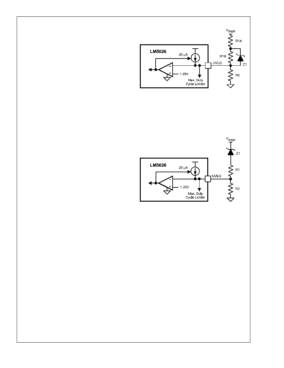
VOLTAGE DEPENDENT MAXIMUM DUTY CYCLE
As the input source V
PWR
increases the voltage at the UVLO
pin increases proportionately. To limit the Volt x Seconds
applied to the transformer, the maximum allowed PWM duty
cycle decreases as the UVLO voltage increases. If it is
desired to increase the slope of the voltage limited duty cycle
characteristic, two possible configurations are shown in Fig-
ure 17. After the LM5026 is enabled, the zener diode causes
the UVLO pin voltage to increase more rapidly with increas-
ing input voltage (V
PWR
). The voltage dependent maximum
duty cycle clamp varies with the UVLO pin voltage according
to the following equation:
Voltage-Dependent Duty Cycle (%) = 107 - 21.8 X UVLO
Programmable Maximum Duty Cycle Clamp (DCL)
When the UVLO pin is biased at 1.25V (minimum operating
level), the maximum duty cycle of OUT_A is limited by the
duty cycle of the internal clock signal. The duty cycle of the
internal clock can be adjusted by programming a voltage set
at the DCL pin. The default maximum duty cycle (80%) can
be selected by connecting the DCL pin to the RT pin. The
DCL pin should not be left open. A small decoupling capaci-
tor located close to the DCL pin is recommended.
The oscillator frequency set resistance (R
T
) must be deter-
mined first before programming the maximum duty cycle.
Following the selection of the total R
T
resistance, the ratio of
the R
T
resistors can be designed to set the desired maxi-
mum duty cycle. As the UVLO pin voltage increases from
1.25V, the maximum duty cycle is reduced by the voltage
dependent duty cycle limiter previously as described and
illustrated in Figure 6.
Printed Circuit Board Layout
The LM5026 Current Sense and PWM comparators are very
fast, and respond to short duration noise pulses. The com-
ponents at the CS, COMP, SS, DCL, UVLO, TIME, SYNC
20147931
FIGURE 17. Altering the Slope of Duty Cycle vs. V
PWR
LM5026
www.national.com
19

Applications Information
(Continued)
and the RT pins should be as physically close as possible to
the IC, thereby minimizing noise pickup on the PC board
tracks.
Layout considerations are critical for the current sense filter.
If a current sense transformer is used, both leads of the
transformer secondary should be routed to the sense filter
components and to the IC pins. The ground side of each
transformer should be connected via a dedicated PC board
track to the AGND pin, rather than through the ground plane.
If the current sense circuit employs a sense resistor in the
drive transistor source, low inductance resistor should be
used. In this case, all the noise sensitive low current ground
tracks should be connected in common near the IC, and then
a single connection made to the power ground (sense resis-
tor ground point). The gate drive outputs of the LM5026
should have short direct paths to the power MOSFETs in
order to minimize inductance in the PC board traces.
The two ground pins (AGND, PGND) must be connected
together with a short direct connection to avoid jitter due to
relative ground bounce.
If the internal dissipation of the LM5026 produces high junc-
tion temperatures during normal operation, the use of mul-
tiple vias under the IC to a ground place can help conduct
heat away from the IC. Judicious positioning of the PC board
within the end product, along with use of any available air
flow (forced or natural convection) can help reduce the junc-
tion temperatures.
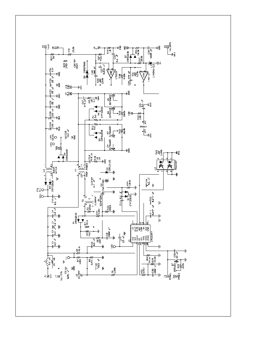
Application Circuit Example
The following schematic shows an example of an LM5026
controlled 100W active clamp forward power converter. The
input voltage range (V
PWR
) is 36V to 78V, and the output
voltage is 3.3V. The output current capability is 30 Amps.
Current sense transformer T2 provides information to the CS
pin for current mode control and current limit protection. The
error amplifiers and reference U3 and U4 provide voltage
feedback via optocoupler U2. Synchronous rectifiers Q3-Q6
minimize rectification losses in the secondary. An auxiliary
winding on inductor L2 provides power to the LM5026 VCC
pin when the output is in regulation. The input voltage UVLO
levels are
34V for increasing V
PWR
, and
32V for decreas-
ing V
PWR
. The circuit can be shut down by forcing the
ON/OFF input (J2) below 1.25V. An external synchronizing
frequency can be applied to the SYNC input (J11) or like
converters can be self-synchronized by connections of (J3).
The regulator output is current limited at
32A.
LM5026
www.national.com
20
Applications
Information
(Continued)
20147932
FIGURE
18.
Application
Circuit:
Input
36-78V
,
Output
3.3V
,
30A
LM5026
www.national.com
21
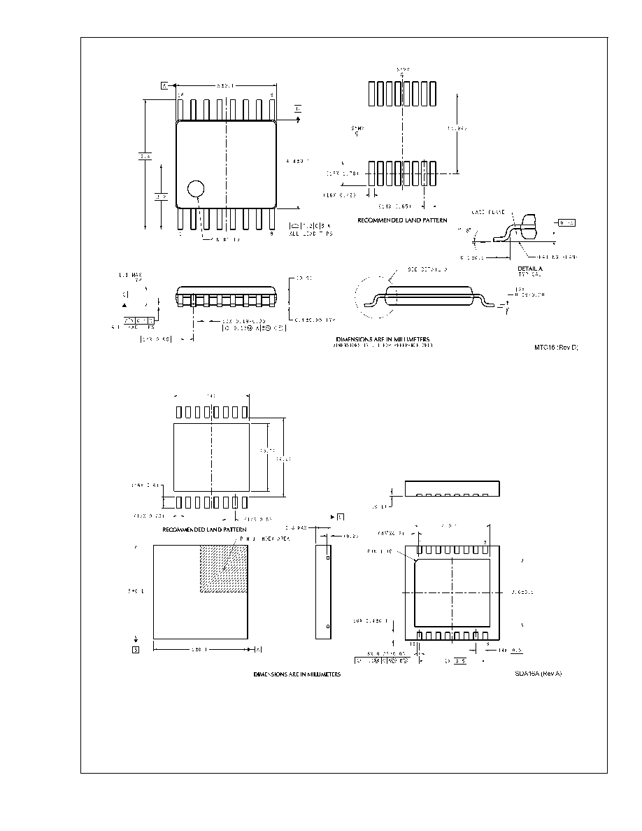
Physical Dimensions
inches (millimeters) unless otherwise noted
Molded TSSOP-16
NS Package Number MTC16
Note: It is recommended that the exposed pad be connected to Pin 11 (AGND).
16-Lead LLP Surface Mount Package
NS Package Number SDA16A
LM5026
www.national.com
22

Notes
National does not assume any responsibility for use of any circuitry described, no circuit patent licenses are implied and National reserves
the right at any time without notice to change said circuitry and specifications.
For the most current product information visit us at www.national.com.
LIFE SUPPORT POLICY
NATIONAL'S PRODUCTS ARE NOT AUTHORIZED FOR USE AS CRITICAL COMPONENTS IN LIFE SUPPORT DEVICES OR SYSTEMS
WITHOUT THE EXPRESS WRITTEN APPROVAL OF THE PRESIDENT AND GENERAL COUNSEL OF NATIONAL SEMICONDUCTOR
CORPORATION. As used herein:
1. Life support devices or systems are devices or systems
which, (a) are intended for surgical implant into the body, or
(b) support or sustain life, and whose failure to perform when
properly used in accordance with instructions for use
provided in the labeling, can be reasonably expected to result
in a significant injury to the user.
2. A critical component is any component of a life support
device or system whose failure to perform can be reasonably
expected to cause the failure of the life support device or
system, or to affect its safety or effectiveness.
BANNED SUBSTANCE COMPLIANCE
National Semiconductor manufactures products and uses packing materials that meet the provisions of the Customer Products
Stewardship Specification (CSP-9-111C2) and the Banned Substances and Materials of Interest Specification (CSP-9-111S2) and contain
no ``Banned Substances'' as defined in CSP-9-111S2.
Leadfree products are RoHS compliant.
National Semiconductor
Americas Customer
Support Center
Email: new.feedback@nsc.com
Tel: 1-800-272-9959
National Semiconductor
Europe Customer Support Center
Fax: +49 (0) 180-530 85 86
Email: europe.support@nsc.com
Deutsch Tel: +49 (0) 69 9508 6208
English
Tel: +44 (0) 870 24 0 2171
FranÁais Tel: +33 (0) 1 41 91 8790
National Semiconductor
Asia Pacific Customer
Support Center
Email: ap.support@nsc.com
National Semiconductor
Japan Customer Support Center
Fax: 81-3-5639-7507
Email: jpn.feedback@nsc.com
Tel: 81-3-5639-7560
www.national.com
LM5026
Active
Clamp
Current
Mode
PWM
Controller