 | –≠–ª–µ–∫—Ç—Ä–æ–Ω–Ω—ã–π –∫–æ–º–ø–æ–Ω–µ–Ω—Ç: LM5030MMX | –°–∫–∞—á–∞—Ç—å:  PDF PDF  ZIP ZIP |
LM5030
100V Push-Pull Current Mode PWM Controller
General Description
The LM5030 High Voltage PWM controller contains all of the
features needed to implement Push-Pull and Bridge topolo-
gies, using current-mode control in a small 10 pin package.
This device provides two alternating gate driver outputs. The
LM5030 includes a high-voltage start-up regulator that oper-
ates over a wide input range of 14V to 100V. Additional
features include: error amplifier, precision reference, dual
mode current limit, slope compensation, softstart, sync ca-
pability and thermal shutdown. This high speed IC has total
propagation delays less than 100ns and a 1MHz capable
single resistor adjustable oscillator.
Package: MSOP-10 (Contact factory for thermally enhanced
LLP availability).
Features
n
Internal High Voltage Start-up Regulator
n
Single Resistor Oscillator Setting
n
Synchronizable
n
Error Amplifier
n
Precision Reference
n
Adjustable Softstart
n
Dual Mode Over-Current Protection
n
Slope Compensation
n
Direct Optocoupler Interface
n
1.5A Peak Gate Drivers
n
Thermal Shutdown
Applications
n
Telecommunication Power Converters
n
Industrial Power Converters
n
+42V Automotive Systems
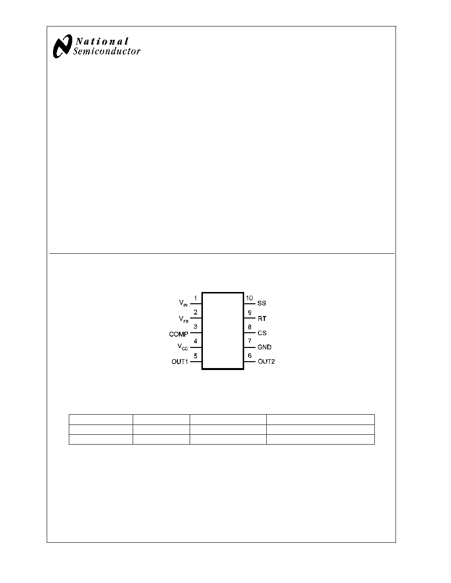
Connection Diagram
Top View
20058112
10-Lead MSOP
Ordering Information
Order Number
Package Marking
NSC Package Drawing
Supplies As
LM5030MM
S73B
MUB10A
1000 Units on Tape and Reel
LM5030MMX
S73B
MUB10A
3500 Units on Tape and Reel
August 2003
LM5030
100V
Push-Pull
Current
Mode
PWM
Controller
© 2003 National Semiconductor Corporation
DS200581
www.national.com
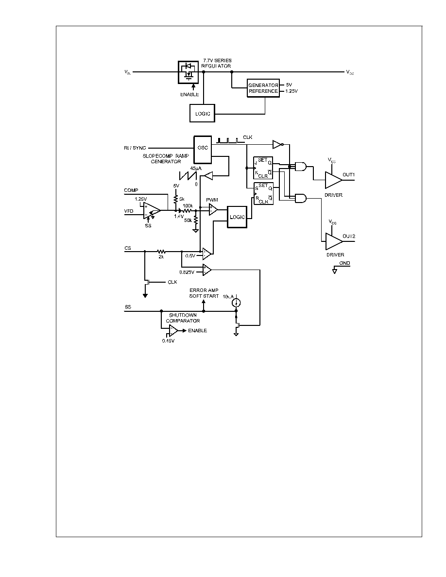
Block Diagram
20058101
FIGURE 1.
LM5030
www.national.com
2
Pin Description
Pin Name
Pin
Number
Description
Application Information
V
IN
1
Source Input Voltage
Input to start-up regulator. Input range 14 to 100 Volts.
V
FB
2
Inverting input to the error amplifier The non-inverting input is internally connected to a 1.25 Volt
reference.
COMP
3
Output to the error amplifier
There is an internal 5K resistor pull-up on this pin. The error
amplifier provides an active sink.
Vcc
4
Output from the internal high
voltage series pass regulator. The
regulation setpoint is 7.7 Volts.
If an auxiliary winding raises the voltage on this pin above the
regulation setpoint the internal series pass regulator will
shutdown, reducing the IC power dissipation.
OUT1
5
Output of the PWM controller
Alternating PWM output gate driver.
OUT2
6
Output of the PWM controller
Alternating PWM output gate driver.
GND
7
Return
Ground
CS
8
Current sense input
Current sense input for current mode control and current limit
sensing. Using separate dedicated comparators, if CS exceeds
0.5 Volt the outputs will go into Cycle by Cycle current limit. If CS
exceeds 0.625V the outputs will be disabled and a softstart
commenced.
RT
9
Oscillator timing resistor pin and
synchronization input.
An external resistor sets the oscillator frequency. This pin will
also accept synchronization pulses from an external oscillator.
SS
10
Dual purpose Softstart and
Shutdown pin
A 10µA current source and an external capacitor set the softstart
timing length. The controller will enter a low power state if the SS
pin is pulled below the typical shutdown threshold of 0.45V.
LM5030
www.national.com
3
Absolute Maximum Ratings
(Note 1)
If Military/Aerospace specified devices are required,
please contact the National Semiconductor Sales Office/
Distributors for availability and specifications.
V
IN
to GND (Survival)
-0.3V to 100V
V
CC
to GND (Survival)
-0.3V to 16V
RT to GND (Survival)
-0.3V to 5.5V
All other pins to GND (Survival)
-0.3V to 7V
Power Dissipation (Note 2)
Internally Limited
ESD Rating (Note 3)
Human Body Model
Machine Model
2kV
200V
Lead Temperature
(Soldering 4 seconds)
260∞C
Storage Temperature Range
-55∞C to +150∞C
Junction Temperature
150∞C
Operating Ratings
Junction Temperature
-40∞C to +105∞C
V
IN
14V to 90V
Electrical Characteristics
Specifications in standard type face are for T
J
= +25∞C and those in boldface type apply over the full operating junction tem-
perature range. Unless otherwise specified: V
IN
= 48V, V
CC
= 10V, and RT = 26.7K
Symbol
Parameter
Conditions
Min
(Note 4)
Typ
(Note 5)
Max
(Note 4)
Units
Startup Regulator
V
CC
Reg
V
CC
Regulation
open ckt
7.4
7.7
8.0
V
V
CC
Current Limit
(Note 2)
10
17
mA
I-V
IN
Startup Regulator Leakage
(external Vcc Supply)
V
IN
= 90V
150
500
µA
I
IN
Shutdown Current
SS = 0V, V
CC
= open
250
350
µA
V
CC
Supply
V
CC
undervoltage Lockout
Voltage
VccReg
- 300mV
VccReg -
100mV
V
Undervoltage Hysteresis
1.2
1.6
2.1
V
I
CC
Supply Current
Cload = 0
2
3
mA
Error Amplifier
GBW
Gain Bandwidth
4
MHz
DC Gain
75
dB
Input Voltage
V
FB
= COMP
1.220
1.245
1.270
V
COMP Sink Capability
V
FB
= 1.5V COMP= 1V
5
13
mA
Current Limit
CS1
Cycle by Cycle CS Threshold
Voltage
0.45
0.5
0.55
V
CS2
Restart CS Threshold Voltage
Resets SS capacitor; auto
restart
0.575
0.625
0.675
V
ILIM Delay to Output
CS step from 0 to 0.6V
Time to onset of OUT
Transition (90%)
Cload = 0
30
ns
CS Sink Current (clocked)
CS = 0.3V
3
6
mA
Soft Start/Shutdown
Softstart Current Source
7
10
13
µA
Softstart to COMP Offset
0.25
0.5
0.75
V
Shutdown Threshold
0.2
0.45
0.7
V
LM5030
www.national.com
4
Electrical Characteristics
(Continued)
Specifications in standard type face are for T
J
= +25∞C and those in boldface type apply over the full operating junction tem-
perature range. Unless otherwise specified: V
IN
= 48V, V
CC
= 10V, and RT = 26.7K
Symbol
Parameter
Conditions
Min
(Note 4)
Typ
(Note 5)
Max
(Note 4)
Units
Oscillator
Frequency1 (RT = 26.7K)
175
200
225
kHz
Frequency2 (RT = 8.2K)
510
600
690
kHz
Sync threshold
3.2
3.8
V
PWM Comparator
Delay to Output
COMP set to 2V CS
stepped 0 to 0.4V, Time
to onset of OUT transition
low
30
ns
Max Duty Cycle
Inferred from deadtime
47.5
49
50
%
Min Duty Cycle
COMP=0V
0
%
COMP to PWM Comparator
Gain
0.34
COMP Open Circuit Voltage
V
FB
= 0V
4.3
5.2
6.1
V
COMP Short Circuit Current
V
FB
= 0V, COMP=0V
0.6
1.1
1.5
mA
Slope Compensation
Slope Comp Amplitude
Delta increase at PWM
Comparator to CS
80
105
130
mV
Output Section
Deadtime
Cload = 0, 10% to 10%
85
135
185
ns
Output High Saturation
Iout = 50mA, V
CC
- V
OUT
0.25
0.75
V
Output Low Saturation
I
OUT
= 100mA
0.25
0.75
V
Rise Time
Cload = 1nF
16
ns
Fall Time
Cload = 1nF
16
ns
Thermal Shutdown
Tsd
Thermal Shutdown Temp.
165
∞C
Thermal Shutdown Hysteresis
15
∞C
Note 1: Absolute Maximum Ratings are limits beyond which damage to the device may occur. Operating Ratings are conditions under which operation of the device
is intended to be functional. For guaranteed specifications and test conditions, see the Electrical Characteristics.
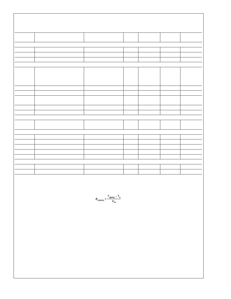
Note 2: The maximum allowable power dissipation is a function of the maximum junction temperature, T
J(MAX)
, the junction-to-ambient thermal resistance,
JA
, and
the ambient temperature, T
A
. The maximum allowable power dissipation at any ambient temperture is calculated using:
Where the value of
JA
for the mini SO-10 (MM) package is 200∞C/W. Exceeding the maximum allowable dissipation will cause excessive die temperature, and the
device will go into thermal shutdown.
Note 3: The human body model is a 100pF capacitor discharged through a 1.5k
resistor into each pin. The machine model is a 200pF capacitor discharged directly
into each pin. The machine model ESD rating for pin 5 and pin 6 is 150V.
Note 4: Limits are 100% production tested at 25∞C. Limits over the operating temperature range are guaranteed through correlation using Statistical Quality Control
(SQC) methods. The limits are used to calculate National's Average Outgoing Quality Level (AOQL).
Note 5: Typical numbers represent the most likely parametric norm for 25∞C operation.
LM5030
www.national.com
5