 | ÐлекÑÑоннÑй компоненÑ: LM5032 | СкаÑаÑÑ:  PDF PDF  ZIP ZIP |
Äîêóìåíòàöèÿ è îïèñàíèÿ www.docs.chipfind.ru
LM5032
High Voltage Dual Interleaved Current Mode Controller
General Description
The LM5032 dual current mode PWM controller contains all
the features needed to control either two independent for-
ward dc/dc converters or a single high current converter
comprised of two interleaved power stages. The two control-
ler channels operate 180° out of phase thereby reducing
input ripple current. The LM5032 includes a startup regulator
that operates over a wide input range up to 100V and
compound (bipolar + CMOS) gate drivers that provide a
robust 2.5A peak sink current. The adjustable maximum
PWM duty cycle reduce stress on the primary side MOSFET
switches. Additional features include programmable line
under-voltage lockout, cycle-by-cycle current limit, hiccup
mode fault operation with adjustable response time, PWM
slope compensation, soft-start, and a 2 MHz capable oscil-
lator with synchronization capability.
Features
n
Two independent PWM current mode controllers
n
Integrated high voltage startup regulator
n
Compound 2.5A main output gate drivers
n
Single resistor oscillator setting to 2 MHz
n
Synchronizable oscillator
n
Programmable maximum duty cycle
n
Maximum duty cycle fold-back at high line voltage
n
Adjustable timer for hiccup mode current limiting
n
Integrated slope compensation
n
Adjustable line under-voltage lockout
n
Independently adjustable soft-start (each regulator)
n
Direct interface with opto-coupler transistor
n
Thermal shutdown
Applications
n
Telecommunication Power Converters
n
Industrial Power Converters
n
+42V Automotive Systems
Packages
n
TSSOP-16
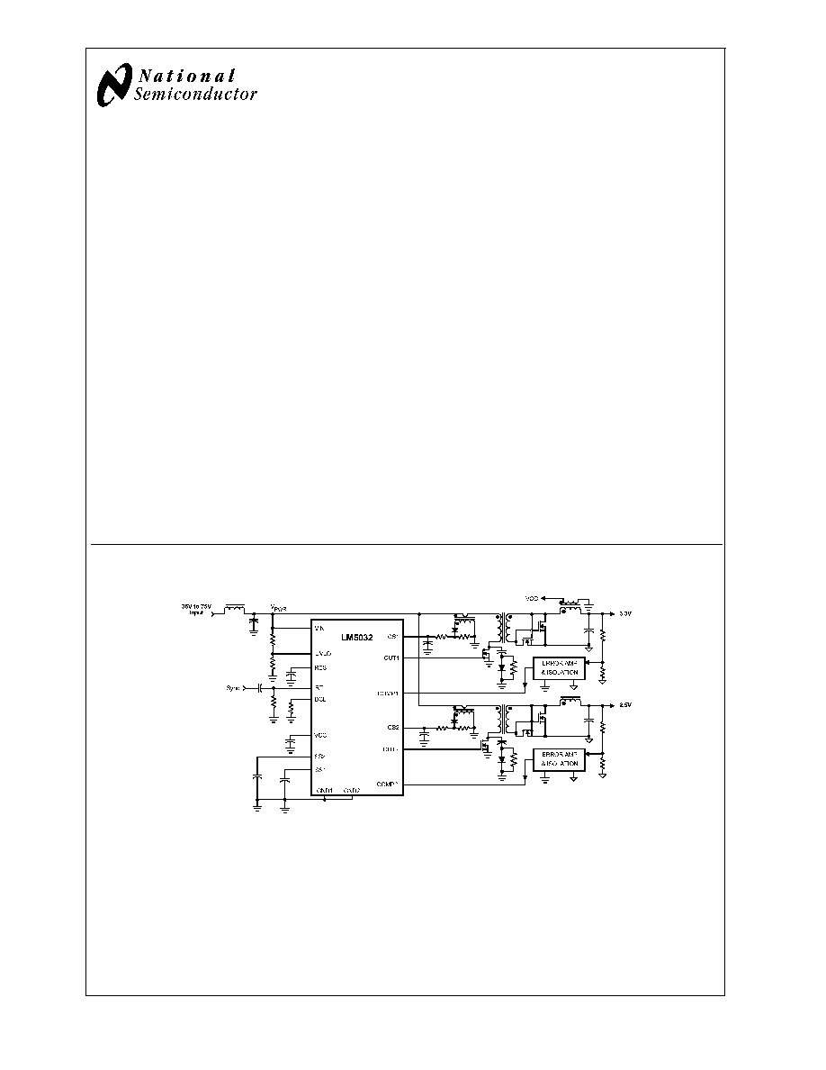
Typical Application Circuit
20135001
Dual Interleaved Regulators with Independent Outputs
March 2005
LM5032
High
V
oltage
Dual
Interleaved
Current
Mode
Controller
© 2005 National Semiconductor Corporation
DS201350
www.national.com
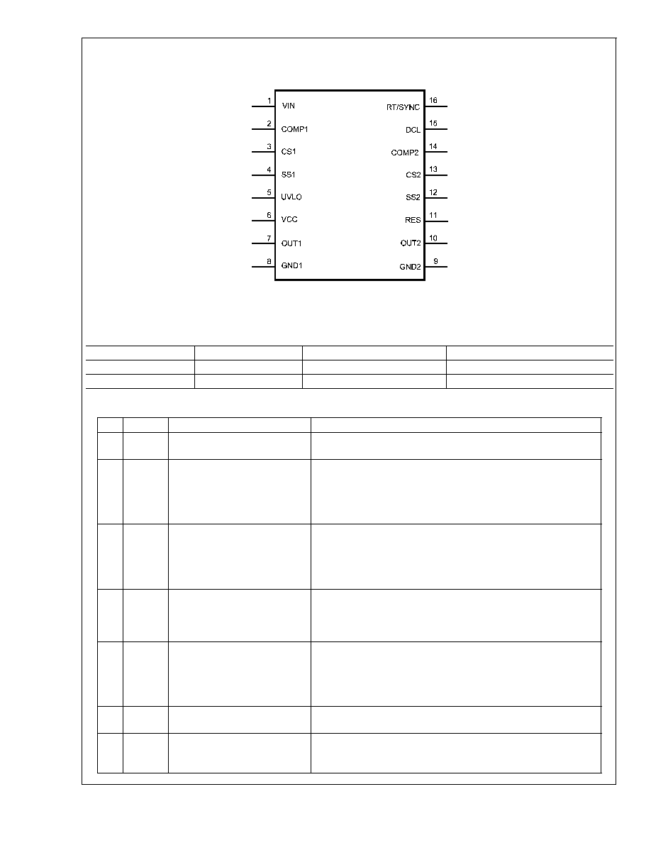
Connection Diagram
Top View
20135002
16-Lead TSSOP
Ordering Information
Order Number
Package Type
NSC Package Drawing
Supplied As
LM5032MTC
TSSOP-16
MTC-16
92 Units per Rail
LM5032MTCX
TSSOP-16
MTC-16
2500 Units on Tape and Reel
Pin Description
PIN
NAME
DESCRIPTION
APPLICATIONS INFORMATION
1
VIN
Input Supply
Input to the startup regulator. The operating input range is 13V to
100V with transient capability to 105V.
2
COMP1
PWM Control, Controller 1
The COMP1 input provides voltage feedback to the PWM comparator
inverting input of Controller 1 through a 3:1 divider. The OUT1 duty
cycle increases as the COMP1 voltage increases. An internal 5K
pull-up resistor to +5.0V provides bias current to an opto-coupler
transistor.
3
CS1
Current Sense Input, Controller 1
Input for current mode control and the current limit sensing. If the CS1
pin exceeds 0.5V the OUT1 pulse is terminated producing
cycle-by-cycle current limiting. External resistance connected to CS1
will adjust (increase) PWM slope compensation. This pin's voltage
must not exceed 1.25V.
4
SS1
Soft-start, Controller 1
An internal 50 µA current source charges an external capacitor to set
the soft-start rate. During a current limit restart sequence, the internal
current source is reduced to 1 µA to increase the delay before retry.
Forcing SS1 below 0.5V shuts off Controller 1.
5
UVLO
VIN Under-Voltage Lockout
An external resistor divider sets the input voltage threshold to enable
the LM5032. The UVLO comparator reference voltage is 1.25V. A
switched 20 µA current source provides adjustable UVLO hysteresis.
The UVLO pin voltage also controls the maximum duty cycle as
described in the Functional Description section.
6
VCC
Start-up regulator output
Output of the 7.7V high voltage start-up regulator. Current limit is a
minimum of 19 mA.
7
OUT1
Main Gate Driver, Controller 1
Gate driver output to the primary side switch for Controller 1. OUT1
swings between VCC and GND1 at a frequency equal to half the
oscillator frequency.
LM5032
www.national.com
2
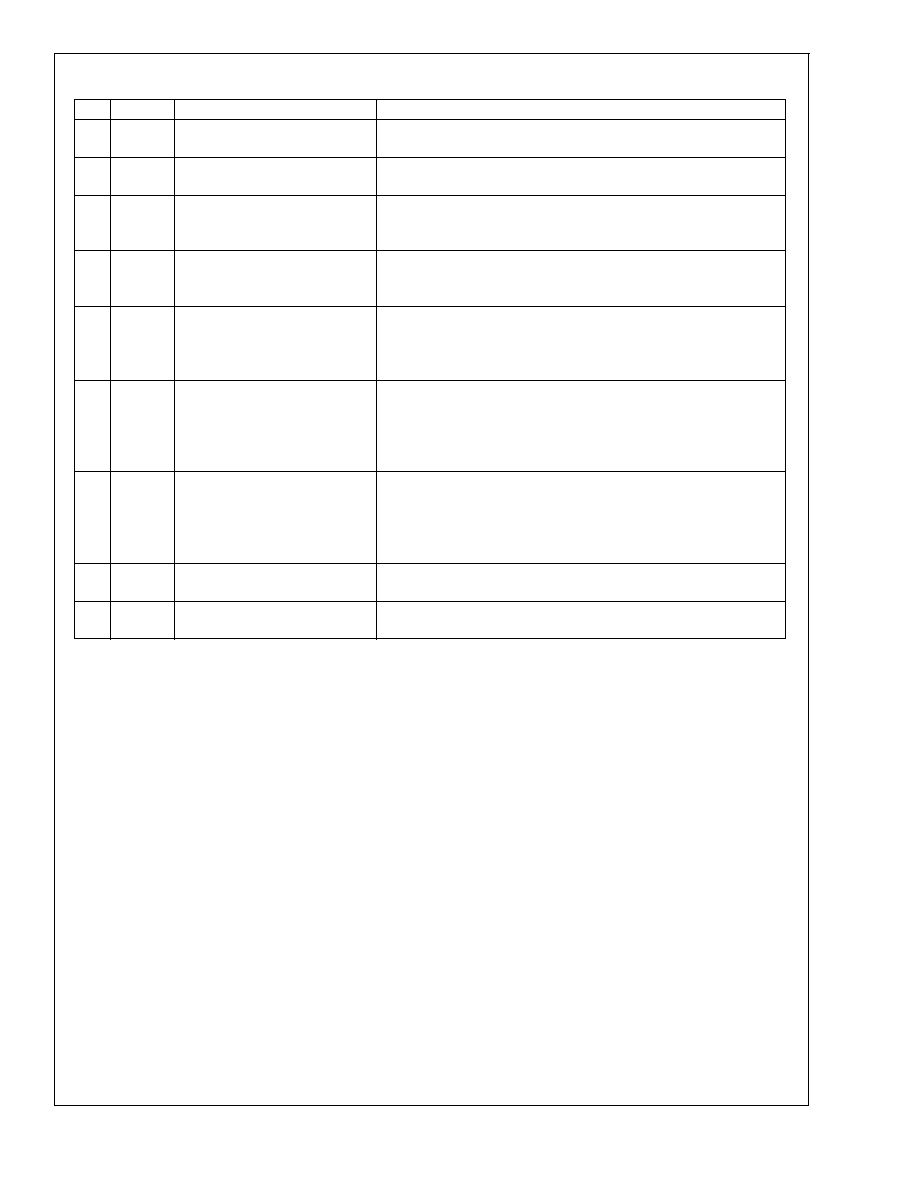
Pin Description
(Continued)
PIN
NAME
DESCRIPTION
APPLICATIONS INFORMATION
8
GND1
Ground, Controller 1
Ground connection for Controller 1 including gate driver, PWM
controller, soft-start and support functions.
9
GND2
Ground, Controller 2
Ground connection for Controller 2 including the gate driver, PWM
controller and soft-start.
10
OUT2
Main Gate Driver, Controller 2
Gate driver output to the primary side switch for Controller 2. OUT2
swings between VCC and GND2 at a frequency equal to half the
oscillator frequency.
11
RES
Hiccup mode restart adjust
An external capacitor sets the time delay before forced restart during a
sustained period of cycle-by-cycle current limiting. The hiccup mode
comparator threshold is 2.55V.
12
SS2
Soft-start, Controller 2
An internal 50 µA current source charges an external capacitor to set
the soft-start rate. During a current limit restart sequence, the internal
current source is reduced to 1µA to increase the delay before retry.
Forcing SS2 below 0.5V shuts off Controller 2.
13
CS2
Current Sense Input, Controller 2
Input for current mode control and the current limit sensing. If the CS2
pin exceeds 0.5V the OUT2 pulse is terminated producing
cycle-by-cycle current limiting. External resistance connected to CS2
will adjust (increase) PWM slope compensation. This pin's voltage
must not exceed 1.25V.
14
COMP2
PWM Control, Controller 2
The COMP2 input provides voltage feedback to the PWM comparator
inverting input of Controller 2 through a 3:1 divider. The OUT2 duty
cycle increases as the COMP2 voltage increases. An internal 5k
pull-up resistor to +5.0V provides bias current to the opto-coupler
transistor.
15
DCL
Duty Cycle Limit
An external resistor sets the maximum allowed duty cycle at OUT1
and OUT2.
16
RT/SYNC Oscillator Adjust and
Synchronizing input
An external resistor sets the oscillator frequency. This pin also accepts
ac-coupled synchronization pulses from an external source.
LM5032
www.national.com
3
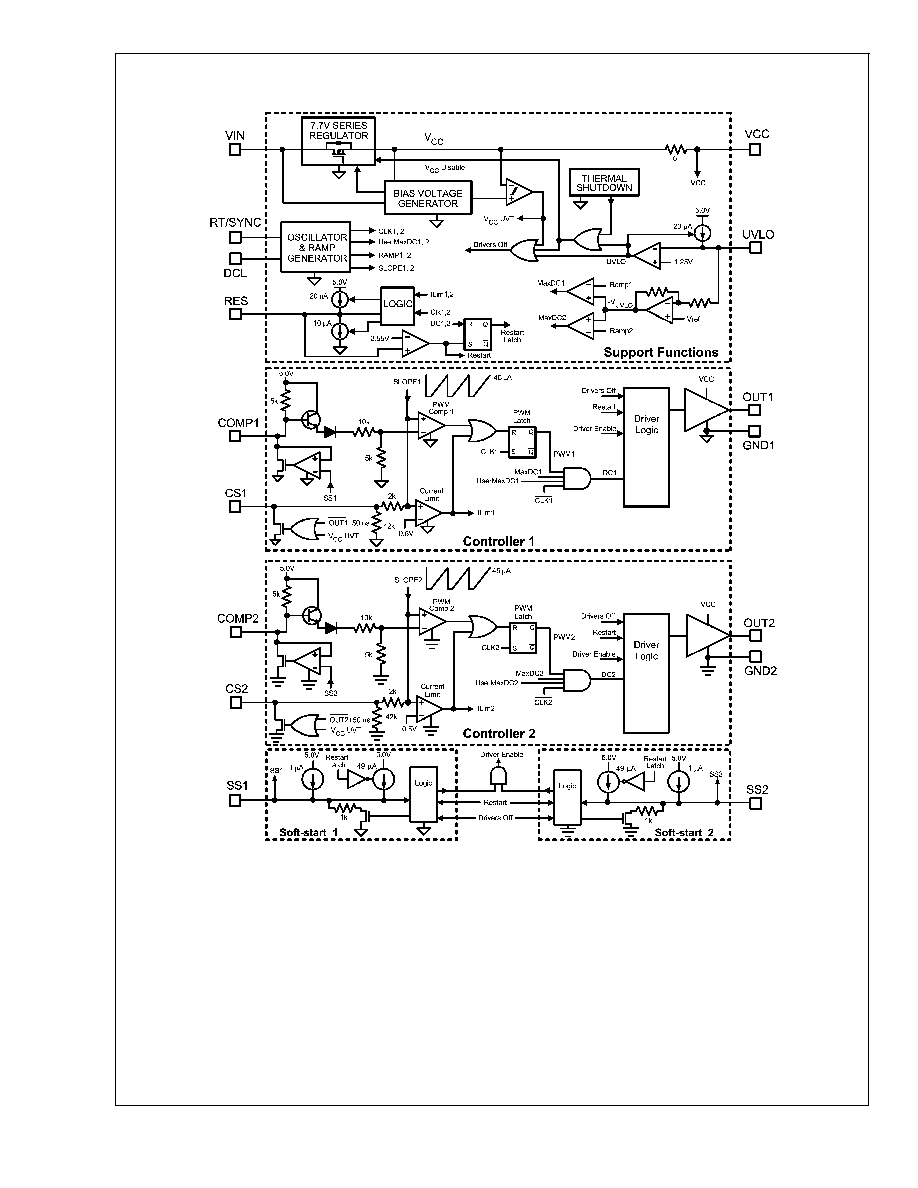
Block Diagram
20135003
FIGURE 1. Detailed Block Diagram
LM5032
www.national.com
4
Absolute Maximum Ratings
(Note 1)
If Military/Aerospace specified devices are required,
please contact the National Semiconductor Sales Office/
Distributors for availability and specifications.
VIN to GND
-0.3V to 105V
VCC to GND
-0.3V to 16V
RT/SYNC, RES and DCL to GND
-0.3V to 5.5V
CS Pins to GND
-0.3V to 1.25V
All other inputs to GND
-0.3V to 7V
ESD Rating (Note 5)
Human Body Model
2kV
Storage Temperature Range
-55°C to 150°C
Junction Temperature
150°C
Lead Temperature (Soldering 4 sec),
(Note 2)
260°C
Operating Ratings
(Note 1)
VIN Voltage
13.0V to 100V
External Voltage Applied to VCC
8V to 15V
Operating Junction Temperature
-40°C to +125°C
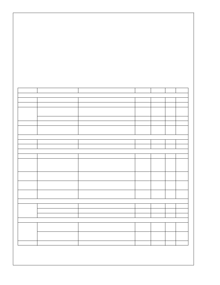
Electrical Characteristics
Specifications with standard typeface are for T
J
= 25°C, and those with boldface type apply over full Operating Junction
Temperature range. VIN = 48V, VCC = 10V externally applied, R
T
= R
DCL
= 42.2k
, UVLO = 1.5V, unless otherwise
stated (Note 3) and (Note 4).
Symbol
Parameter
Conditions
Min
Typ
Max
Units
Startup Regulator (VIN, VCC Pins)
V
CC
Reg
V
CC
voltage
Ext. supply disconnected.
7.4
7.7
8
V
I
CC(Lim)
V
CC
current limit
VCC = 0V.
19
22
mA
V
CC
UVT
V
CC
Under-voltage threshold
(V
CC
increasing)
Ext. supply disconnected, VIN =11V.
VCC -
300 mV
VCC -
100 mV
V
V
CC
decreasing
5.5
6.2
6.9
V
I
IN
Startup regulator current
VIN = 90V, UVLO = 0V
500
600
µA
I
CC
In
Supply current into VCC
from external source
Output loads = open, V
CC
= 10V
4.3
7
mA
UVLO
UVLO
Under-voltage threshold
1.22
1.25
1.28
V
I
HYST
Hysteresis current
16
20
24
µA
Current Sense Input (CS1, CS2 Pins)
CS
Current Limit Threshold
0.45
0.5
0.55
V
CS delay to output
CS1 (CS2) taken from zero to 1.0V.
Time for OUT1 (OUT2) to fall to 90% of
VCC. Output load = 0 pF.
40
ns
Leading edge blanking time
at CS1 (CS2)
50
ns
CS1 (CS2) sink impedance
(clocked)
Internal pull-down FET on.
30
55
R
CS
Equivalent input resistance
at CS
CS taken from 0.2V to 0.5V, internal
FET off.
42
k
Current Limit Restart (RES Pin)
ResTh
Threshold
2.4
2.55
2.7
V
Charge source current
15
20
25
µA
Discharge sink current
7.5
10
12.5
µA
Soft-start (SS1, SS2 Pins)
I
SS
Current source (normal
operation)
35
50
65
µA
Current source during a
current limit restart
0.7
1
1.3
µA
V
SS
Open circuit voltage
5
V
LM5032
www.national.com
5
Document Outline