 | –≠–ª–µ–∫—Ç—Ä–æ–Ω–Ω—ã–π –∫–æ–º–ø–æ–Ω–µ–Ω—Ç: LM5033SDX | –°–∫–∞—á–∞—Ç—å:  PDF PDF  ZIP ZIP |
LM5033
100V Push-Pull Voltage Mode PWM Controller
General Description
The LM5033 High Voltage PWM controller contains all the
features needed to implement Push-Pull, Half-Bridge, and
Full-Bridge topologies. Applications include closed loop volt-
age mode converters with a highly regulated output voltage,
or an open loop "DC transformer" such as an Intermediate
Bus Converter (IBC) with an efficiency
>
95%. The small 10
pin LLP-10 package with exposed pad provides for efficient
thermal management. Two alternating gate driver outputs
with a guaranteed deadtime are provided. The LM5033 in-
cludes a start-up regulator that operates over a wide input
range of 15V to 100V. Additional features include: precision
voltage reference output, current limit detection, remote
shutdown, softstart, sync capability and thermal shutdown.
This high speed IC has total propagation delays less than
100 ns and a 1MHz capable oscillator.
Features
n
Internal high voltage (100V) start-up regulator
n
Single resistor oscillator setting
n
Synchronizable
n
Precision reference output
n
Adjustable soft-start
n
Over-current protection
n
Direct optocoupler interface
n
1.5A peak gate drivers
n
Thermal Shutdown
Applications
n
Intermediate DC/DC Bus Converter
n
Telecommunication Power Converters
n
Industrial Power Converters
n
+42V Automotive Systems
Package
n
LLP-10
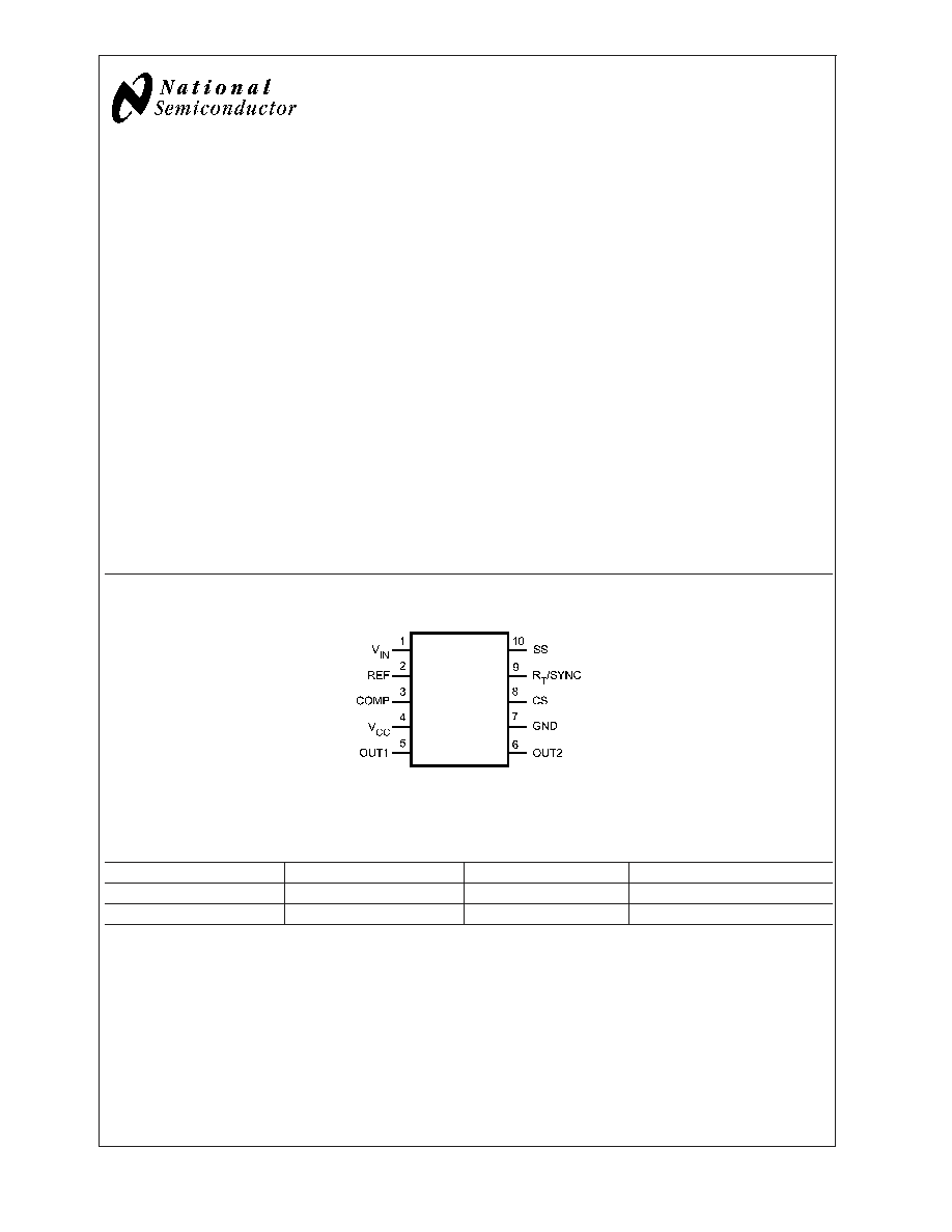
Connection Diagram
20035401
10 -Lead Plastic, Dual, LLP
Ordering Information
Order Number
Package Type
NSC Package Drawing
Supplied As
LM5033SD
LLP-10 (4 x 4 mm)
SDC10A
1000 Units on Tape and Reel
LM5033SDX
LLP-10 (4 x 4 mm)
SDC10A
4500 Units on Tape and Reel
April 2004
LM5033
100V
Push-Pull
V
oltage
Mode
PWM
Controller
© 2004 National Semiconductor Corporation
DS200354
www.national.com
Pin Description
PIN
NAME
DESCRIPTION
APPLICATION INFORMATION
1
Vin
Input Voltage
Input to the start-up regulator. Input range is 15V to
90V, with transient capability to 100V .
2
REF
2.5V precision reference output
Sink only, requires an external pull-up resistor. This
can be used as a reference for external circuitry.
3
COMP
PWM Input
Feedback to the PWM comparator's inverting input,
through a 3:1 divider. The output duty cycle increases
as this pin's voltage increases. Internally there is a
5k
pullup to +5.2V.
4
VCC
9.6V output from the internal high voltage series
pass regulator
An external voltage (10V - 15V) can be applied to this
pin to shutdown the internal regulator, thereby
reducing internal dissipation. An internal diode
connects Vcc to Vin.
5
OUT1
Gate Driver Output #1
Alternating output gate driver, which can source and
sink 1.5A.
6
OUT2
Gate Driver Output #2
Alternating output gate driver, which can source and
sink 1.5A.
7
GND
Ground pin for all internal circuitry
Connections to external ground must be done with
care for optimum performance. See the Functional
Description and Applications Section for more
information.
8
CS
Current sense input
Current sense input for the current limit detection. If
CS exceeds 0.5V the outputs are disabled and the
softstart pin is discharged to ground.
9
R
T
/ SYNC
Oscillator timing resistor pin and synchronization
input
An external resistor to ground sets the oscillator
frequency. This pin will also accept ac-coupled
synchronization pulses from an external source.
10
SS
Softstart pin
An internal 10µA current source and an external
capacitor set the soft-start timing. This pin can be
externally pulled to below 0.5V to disable the output
drivers.
LM5033
www.national.com
2
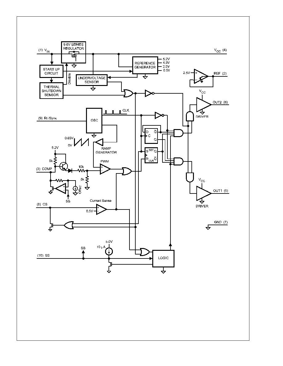
Block Diagram
Functional Block Diagram
20035402
FIGURE 1.
LM5033
www.national.com
3
Absolute Maximum Ratings
(Note 1)
If Military/Aerospace specified devices are required,
please contact the National Semiconductor Sales Office/
Distributors for availability and specifications.
V
IN
to GND
-0.3V to 100V
V
CC
to GND
-0.3V to 16V
Rt/Sync to GND
-0.3V to 5.5V
Pins 3, 8, 10 to GND
-0.3V to 7.0V
ESD Rating (Note 3)
Human Body Model
2kV
Storage Temperature Range
-65∞C to 150∞C
Junction Temperature
150∞C
Power Dissipation (Note 2)
Internally Limited
Operating Ratings
(Note 1)
V
IN
Voltage (Pin1)
15 to 90V
Operating Junction Temperature
-40∞C to 125∞C
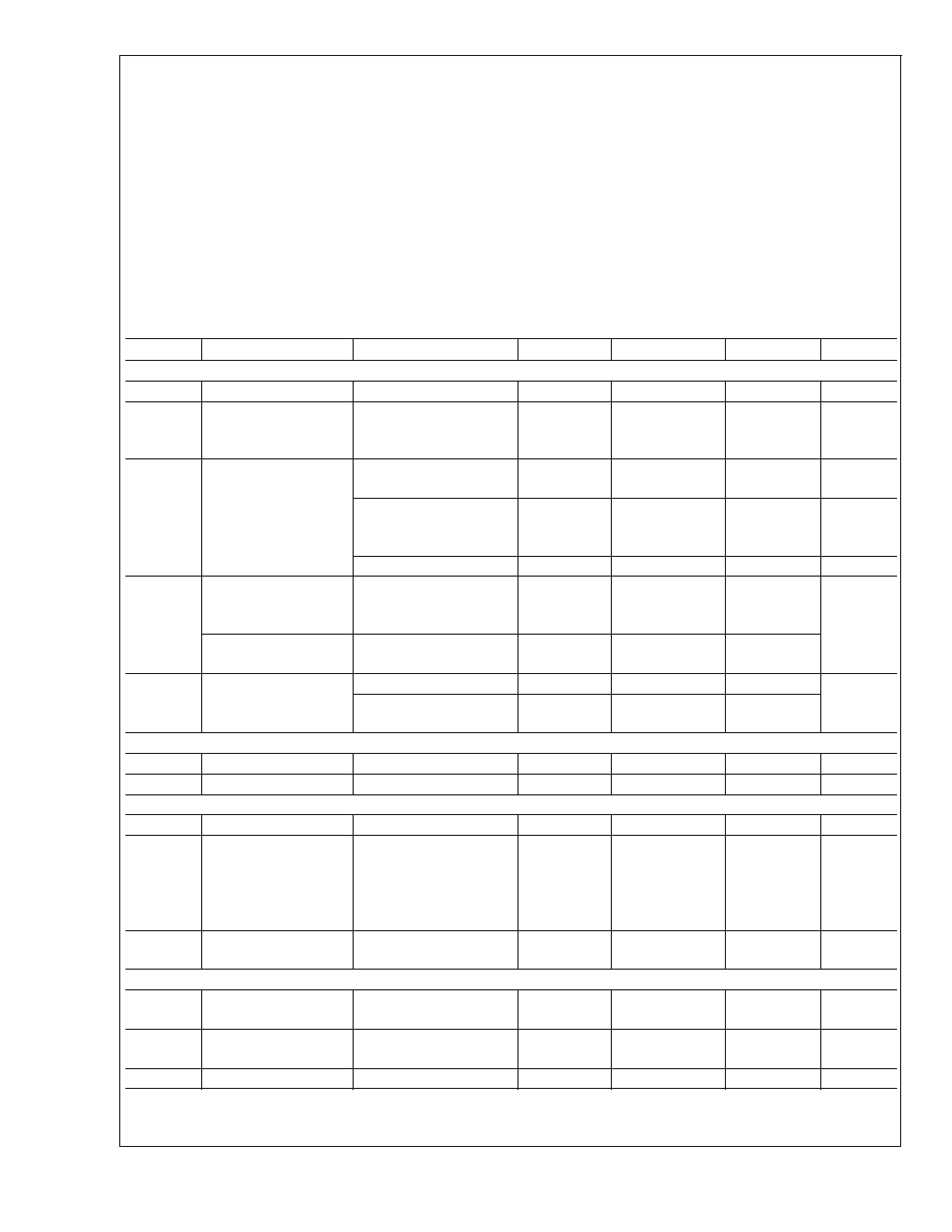
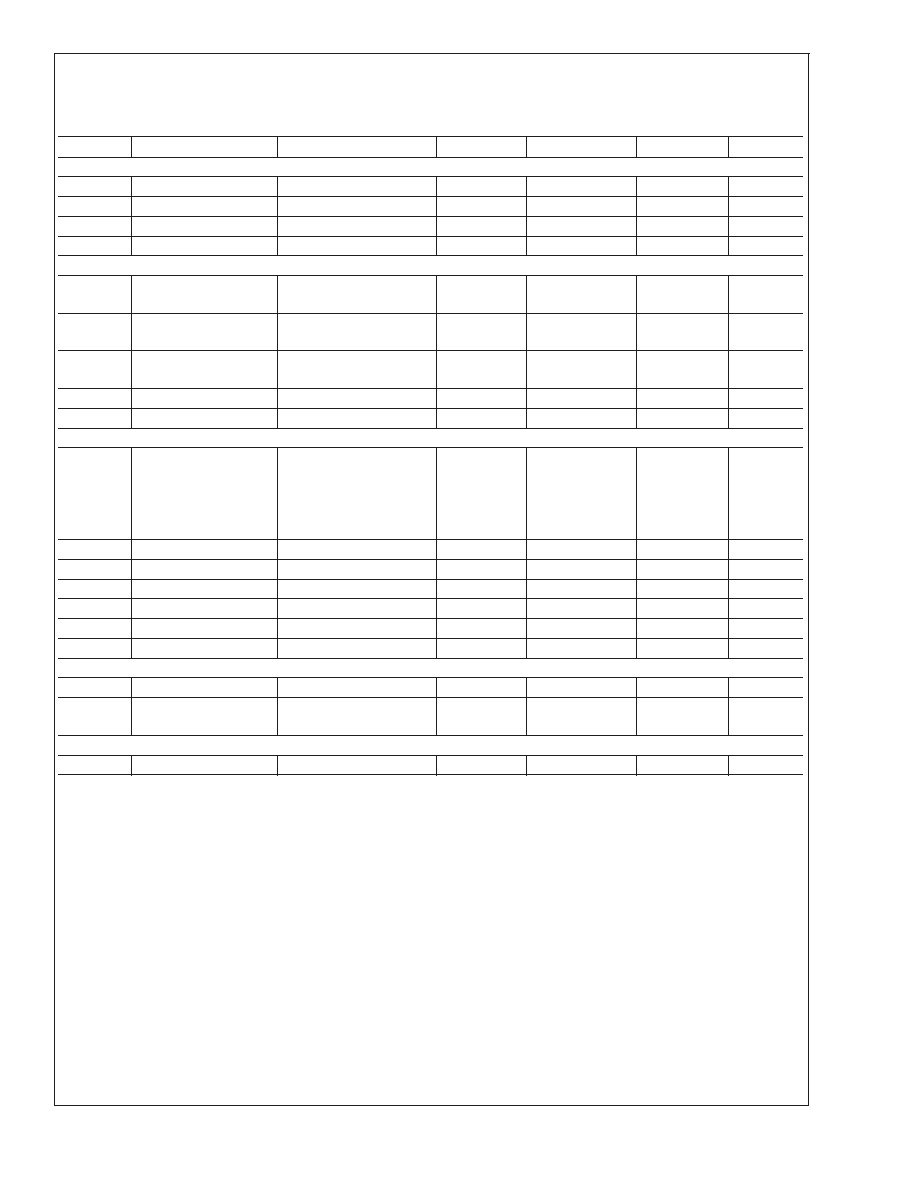
Electrical Characteristics
Specifications with standard typeface are for T
J
= 25∞C, and those with boldface type apply over full Operating Junction
Temperature range. V
IN
= 48V, V
CC
= 10V applied externally, R
T
= 26.7k
, unless otherwise stated. See (Note 4) and (Note
5).
Symbol
Parameter
Conditions
Min
Typ
Max
Units
V
CC
Startup Regulator (Pins 1, 4)
V
CC
Reg
V
CC
Voltage
Pin 4 open
9.2
9.6
10.0
V
Icc-out
V
CC
Current Limit
Out1, Out2 disabled. Ext.
supply to Vcc
disconnected.
20
34
mA
Iin
Startup Regulator
Current into V
IN
Normal Operation
V
IN
= 90V
150
500
µA
Ext. V
CC
Supply
Disconnected and
Output Load = 1800pF
7
mA
SS Pin = 0V
3
mA
UVT
V
CC
Undervoltage
Threshold (increasing
V
CC
)
VccReg -
300mV
VccReg - 100
mV
V
UVT Hysteresis
(decreasing V
CC
)
2.3
2.8
3.3
Icc-in
Supply Current from
external source to V
CC
SS Pin = 0V
2
3
mA
SS Pin = open and
Output Load = 1800pF
7
2.5V Reference (Pin 2)
Vref
Output voltage
Pin 2 sink current = 5mA
2.44
2.50
2.56
V
Current sink capability
5.0
13
mA
Current Sense (Pin 8)
CS
Threshold voltage
0.45
0.50
0.55
V
CS delay to output
Pin 8 taken from zero to
0.6V. Time for Out1 or
Out2 to fall to 90% of
Vcc. CLoad = 0
@
Out1,
Out2
30
ns
Current sink capability
(clocked)
Pin 8
0.3V
3
6
mA
Softstart (Pin 10)
Softstart current
source
7
10
13
µA
Softstart to Comp
offset
0.25
0.50
0.75
V
Open Circuit Voltage
5.0
V
LM5033
www.national.com
4
Electrical Characteristics
(Continued)
Specifications with standard typeface are for T
J
= 25∞C, and those with boldface type apply over full Operating Junction
Temperature range. V
IN
= 48V, V
CC
= 10V applied externally, R
T
= 26.7k
, unless otherwise stated. See (Note 4) and (Note
5).
Symbol
Parameter
Conditions
Min
Typ
Max
Units
Oscillator (Pin 9)
Fs1
Internal frequency
Rt = 26.7 k
175
200
225
kHz
Fs2
Internal frequency
Rt = 8.2 k
600
kHz
Vsync
Sync threshold
3.2
3.8
V
R
t
/Sync DC voltage
2.0
V
PWM Comparator Input (Pin 3)
t
PWM
Gain from pin 3 to
PWM comparator
0.34
V/V
Maximum duty cycle at
Out1, Out2
See PWM Comparator
text
100 x
(0.5T
S
-T
D
)/T
S
%
Minimum duty cycle at
Out1, Out2
Pin 3 = 0V.
0
%
Open Circuit Voltage
4.2
5.2
6.2
V
Short circuit current
Pin 3 = 0V
0.6
1.1
1.5
mA
Output Drivers (Pin 5, 6)
Deadtime (T
D
)
CLoad = 0
@
OUT1,
OUT2. Time measured
from 10% of falling
output to 10% of rising
output.
85
135
185
ns
Rise Time
C
Load
= 1nF
16
ns
Fall Time
C
Load
= 1nF
16
ns
Output High Voltage
Iout = 50 mA (source)
Vcc-0.75
Vcc-0.25
V
Output Low Voltage
Iout = 100 mA (sink)
0.25
0.75
V
Max. source current
1.5
A
Max. sink current
1.5
A
Thermal Shutdown
T
SD
Shutdown temperature
165
∞C
Shutdown temperature
hysteresis
15
∞C
Thermal Resistance
JA
Junction to Ambient
SDC10A Package
38
∞C/W
Note 1: Absolute Maximum Ratings are limits beyond which damage to the device may occur. Operating Ratings are conditions under which operation of the device
is intended to be functional. For guaranteed specifications and test conditions, see the Electrical Characteristics.
Note 2: The maximum allowable power dissipation is a function of the maximum allowed junction temperature (T
J(max)
), the ambient temperature (T
A
), and the
junction-to-ambient thermal resistance (
JA
). The maximum allowable power dissipation can be calculated from PD = (T
J(max)
- T
A
) /
JA
. Excessive power dissipation
will cause the thermal shutdown to activate.
Note 3: The human body model is a 100 pF capacitor discharged through a 1.5k
resistor into each pin.
Note 4: Min and Max limits are 100% production tested at 25∞C. Limits over the operating temperature range are guaranteed through correlation using Statistical
Quality Control (SQC) methods. Limits are used to calculate National's Average Outgoing Quality Level (AOQL).
Note 5: Typical specifications represent the most likely parametric norm at 25∞C operation.
LM5033
www.national.com
5