 | –≠–ª–µ–∫—Ç—Ä–æ–Ω–Ω—ã–π –∫–æ–º–ø–æ–Ω–µ–Ω—Ç: LM5102SDX | –°–∫–∞—á–∞—Ç—å:  PDF PDF  ZIP ZIP |
LM5102
High Voltage Half-Bridge Gate Driver with Programmable
Delay
General Description
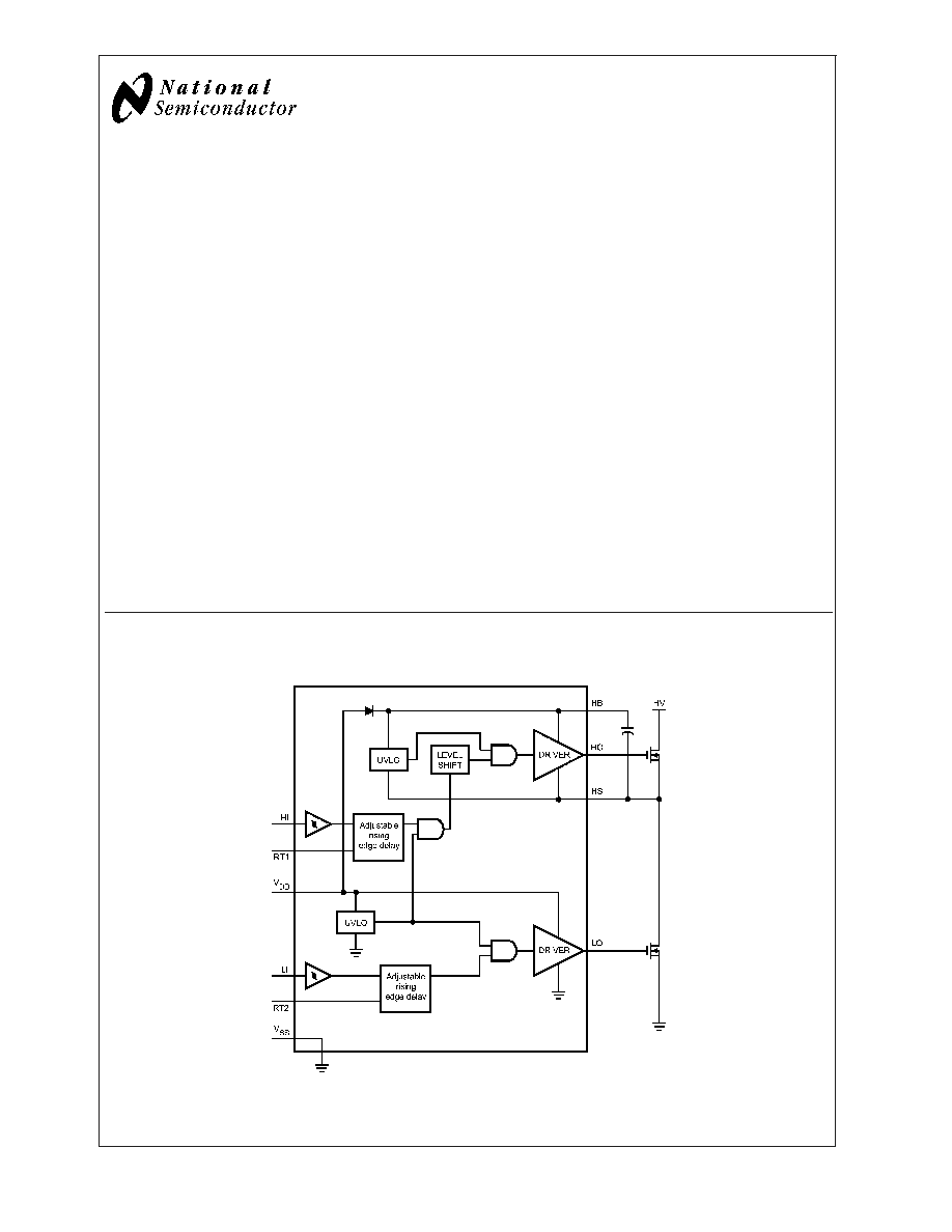
The LM5102 High Voltage Gate Driver is designed to drive
both the high side and the low side N-Channel MOSFETs in
a synchronous buck or a half bridge configuration. The float-
ing high-side driver is capable of working with supply volt-
ages up to 100V. The outputs are independently controlled.
The rising edge of each output can be independently de-
layed with a programming resistor. An integrated high volt-
age diode is provided to charge the high side gate drive
bootstrap capacitor. A robust level shifter operates at high
speed while consuming low power and providing clean level
transitions from control logic to the high side gate driver.
Under-voltage lockout is provided on both the low side and
the high side power rails. This device is available in the
standard MSOP-10 pin and the LLP-10 pin packages.
Features
n
Drives both a high side and low side N-channel
MOSFET
n
Independently programmable high and low side rising
edge delay
n
Bootstrap supply voltage range up to 118V DC
n
Fast turn-off propagation delay (25 ns typical)
n
Drives 1000 pF loads with 15 ns rise and fall times
n
Supply rail under-voltage lockout
n
Low power consumption
n
Timer can be terminated midway through sequence
Typical Applications
n
Current Fed push-pull power converters
n
Half and Full Bridge power converters
n
Synchronous Buck converters
n
Two switch forward power converters
n
Forward with Active Clamp converters
Package
n
MSOP-10
n
LLP-10 (4 mm x 4 mm)
Simplified Block Diagram
20088902
FIGURE 1.
January 2004
LM5102
High
V
oltage
Half-Bridge
Gate
Driver
with
Programmable
Delay
© 2004 National Semiconductor Corporation
DS200889
www.national.com
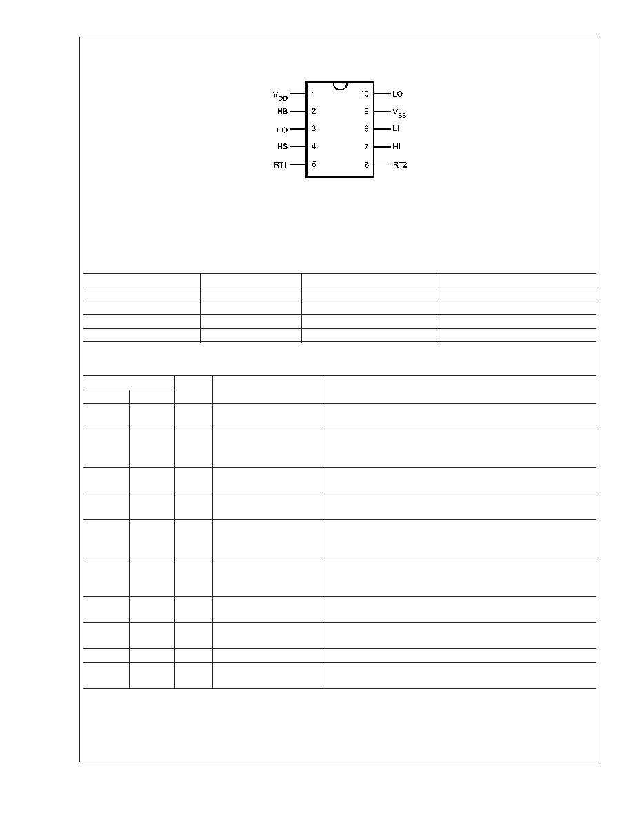
Connection Diagram
Ordering Information
Ordering Number
Package Type
NSC Package Drawing
Supplied As
LM5102MM
MSOP-10
MUB10A
1000 shipped as Tape & Reel
LM5102MMX
MSOP-10
MUB10A
3500 shipped as Tape & Reel
LM5102SD
LLP-10
SDC10A
1000 shipped as Tape & Reel
LM5102SDX
LLP-10
SDC10A
4500 shipped as Tape & Reel
Pin Descriptions
Pin
Name
Description
Application Information
MSOP-10
LLP-10
1
1
V
DD
Positive gate drive supply
Locally decouple to V
SS
using low ESR/ESL capacitor, located as
close to IC as possible.
2
2
HB
High side gate driver
bootstrap rail
Connect the positive terminal of bootstrap capacitor to the HB pin
and connect negative terminal of bootstrap capacitor to HS. The
Bootstrap capacitor should be placed as close to IC as possible.
3
3
HO
High side gate driver
output
Connect to gate of high side MOSFET with short low inductance
path.
4
4
HS
High side MOSFET source
connection
Connect bootstrap capacitor negative terminal and source of high
side MOSFET.
5
5
RT1
High side output edge
delay programming
Resistor from RT1 to ground programs the leading edge delay of
the high side gate driver. The resistor should be placed close to the
IC to minimize noise coupling from adjacent traces.
6
6
RT2
Low side output edge
delay programming
Resistor from RT2 to ground programs the leading edge delay of
the low side gate driver. The resistor should be placed close to the
IC to minimize noise coupling from adjacent traces.
7
7
HI
High side driver control
input
TTL compatible thresholds. Unused inputs should be tied to ground
and not left open.
8
8
LI
Low side driver control
input
TTL compatible thresholds. Unused inputs should be tied to ground
and not left open.
9
9
V
SS
Ground return
All signals are referenced to this ground.
10
10
LO
Low side gate driver output Connect to the gate of the low side MOSFET with a short low
inductance path.
Note: For LLP-10 package, it is recommended that the exposed pad on the bottom of the LM5100 / LM5101 be soldered to ground plane on the PC board,
and the ground plane should extend out from beneath the IC to help dissipate the heat..
20088901
10-Lead MSOP, LLP
See NS Numbers MUB10A and SDC10A
FIGURE 2.
LM5102
www.national.com
2
Absolute Maximum Ratings
(Note 1)
If Military/Aerospace specified devices are required,
please contact the National Semiconductor Sales Office/
Distributors for availability and specifications.
V
DD
to V
SS
≠0.3V to +18V
V
HB
to V
HS
≠0.3V to +18V
LI or HI Inputs to V
SS
≠0.3V to V
DD
+ 0.3V
LO Output
≠0.3V to V
DD
+ 0.3V
HO Output
V
HS
≠ 0.3V to V
HB
+ 0.3V
V
HS
to V
SS
-1V to +100V
V
HB
to V
SS
118V
RT1 & RT2 to V
SS
≠0.3V to 5V
Junction Temperature
+150∞C
Storage Temperature Range
≠55∞C to +150∞C
ESD Rating HBM
(Note 2)
2 kV
Recommended Operating
Conditions
V
DD
+9V to +14V
HS
≠1V to 100V
HB
V
HS
+ 8V to V
HS
+ 14V
HS Slew Rate
<
50V/ns
Junction Temperature
≠40∞C to +125∞C
Electrical Characteristics
Specifications in standard typeface are for T
J
= +25∞C, and those in boldface
type apply over the full operating junction temperature range. Unless otherwise specified, V
DD
= V
HB
= 12V, V
SS
= V
HS
=
0V, RT1 = RT2 = 100k
. No Load on LO or HO.
Symbol
Parameter
Conditions
Min
Typ
Max
Units
SUPPLY CURRENTS
I
DD
V
DD
Quiescent Current
LI = HI = 0V
0.4
0.6
mA
I
DDO
V
DD
Operating Current
f = 500 kHz
1.5
3
mA
I
HB
Total HB Quiescent Current
LI = HI = 0V
0.06
0.2
mA
I
HBO
Total HB Operating Current
f = 500 kHz
1.3
3
mA
I
HBS
HB to V
SS
Current, Quiescent
V
HS
= V
HB
= 100V
0.05
10
µA
I
HBSO
HB to V
SS
Current, Operating
f = 500 kHz
0.08
mA
INPUT PINS
V
IL
Low Level Input Voltage Threshold
0.8
1.8
V
V
IH
High Level Input Voltage Threshold
1.8
2.2
V
R
I
Input Pulldown Resistance
100
200
500
k
TIME DELAY CONTROLS
V
RT
Nominal Voltage at RT1, RT2
2.7
3
3.3
V
I
RT
RT Pin Current Limit
RT1 = RT2 = 0V
0.75
1.5
2.25
mA
V
th
Timer Termination Threshold
1.8
V
T
DL1
, T
DH1
Rising edge turn-on delay, RT = 10 k
75
105
150
ns
T
DL2
, T
DH2
Rising edge turn-on delay, RT = 100 k
530
630
750
ns
UNDER VOLTAGE PROTECTION
V
DDR
V
DD
Rising Threshold
6.0
6.9
7.4
V
V
DDH
V
DD
Threshold Hysteresis
0.5
V
V
HBR
HB Rising Threshold
5.7
6.6
7.1
V
V
HBH
HB Threshold Hysteresis
0.4
V
BOOT STRAP DIODE
V
DL
Low-Current Forward Voltage
I
VDD-HB
= 100 µA
0.60
0.9
V
V
DH
High-Current Forward Voltage
I
VDD-HB
= 100 mA
0.85
1.1
V
R
D
Dynamic Resistance
I
VDD-HB
= 100 mA
0.8
1.5
LO GATE DRIVER
V
OLL
Low-Level Output Voltage
I
LO
= 100 mA
0.25
0.4
V
V
OHL
High-Level Output Voltage
I
LO
= ≠100 mA,
V
OHL
= V
DD
≠ V
LO
0.35
0.55
V
I
OHL
Peak Pullup Current
V
LO
= 0V
1.6
A
I
OLL
Peak Pulldown Current
V
LO
= 12V
1.8
A
HO GATE DRIVER
V
OLH
Low-Level Output Voltage
I
HO
= 100 mA
0.25
0.4
V
LM5102
www.national.com
3
Electrical Characteristics
Specifications in standard typeface are for T
J
= +25∞C, and those in boldface type
apply over the full operating junction temperature range. Unless otherwise specified, V
DD
= V
HB
= 12V, V
SS
= V
HS
= 0V,
RT1 = RT2 = 100k
. No Load on LO or HO. (Continued)
Symbol
Parameter
Conditions
Min
Typ
Max
Units
V
OHH
High-Level Output Voltage
I
HO
= ≠100 mA,
V
OHH
= V
HB
≠ V
HO
0.35
0.55
V
I
OHH
Peak Pullup Current
V
HO
= 0V
1.6
A
I
OLH
Peak Pulldown Current
V
HO
= 12V
1.8
A
THERMAL RESISTANCE
JA
Junction to Ambient
MSOP
200
∞C/W
LLP-10 (Note 3)
40
Switching Characteristics
Specifications in standard typeface are for T
J
= +25∞C, and those in boldface
type apply over the full operating junction temperature range. Unless otherwise specified, V
DD
= V
HB
= 12V, V
SS
= V
HS
=
0V, No Load on LO or HO .
Symbol
Parameter
Conditions
Min
Typ
Max
Units
t
LPHL
Lower Turn-Off Propagation Delay LM5102
(LI Falling to LO Falling)
27
56
ns
t
HPHL
Upper Turn-Off Propagation Delay LM5102
(HI Falling to HO Falling)
27
56
ns
t
RC
, t
FC
Either Output Rise/Fall Time
C
L
= 1000 pF
15
ns
t
R
, t
F
Either Output Rise/Fall Time (3V to 9V)
C
L
= 0.1 µF
0.6
µs
t
BS
Bootstrap Diode Turn-Off Time
I
F
= 20 mA, I
R
= 200 mA
50
ns
Note 1: Absolute Maximum Ratings indicate limits beyond which damage to the component may occur. Operating Ratings are conditions under which operation of
the device is guaranteed. Operating Ratings do not imply guaranteed performance limits. For guaranteed performance limits and associated test conditions, see the
Electrical Characteristics tables.
Note 2: The human body model is a 100 pF capacitor discharged through a 1.5k
resistor into each pin. 2 kV for all pins except Pin 2, Pin 3 and Pin 4 which are
rated at 500V.
Note 3: 4 layer board with Cu finished thickness 1.5/1/1/1.5 oz. Maximum die size used. 5x body length of Cu trace on PCB top. 50 x 50mm ground and power
planes embedded in PCB. See Application Note AN-1187.
Note 4: Min and Max limits are 100% production tested at 25∞C. Limits over the operating temperature range are guaranteed through correlation using Statistical
Quality Control (SQC) methods. Limits are used to calculate National's Average Outgoing Quality Level (AOQL).
Note 5: The
JA
is not a given constant for the package and depends on the printed circuit board design and the operating environment.
LM5102
www.national.com
4
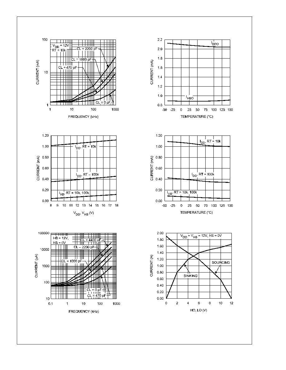
Typical Performance Characteristics
I
DD
vs Frequency
Operating Current vs Temperature
20088910
20088911
Quiescent Current vs Supply Voltage
Quiescent Current vs Temperature
20088912
20088913
I
HB
vs Frequency
HO & LO Peak Output Current vs Output Voltage
20088916
20088917
LM5102
www.national.com
5
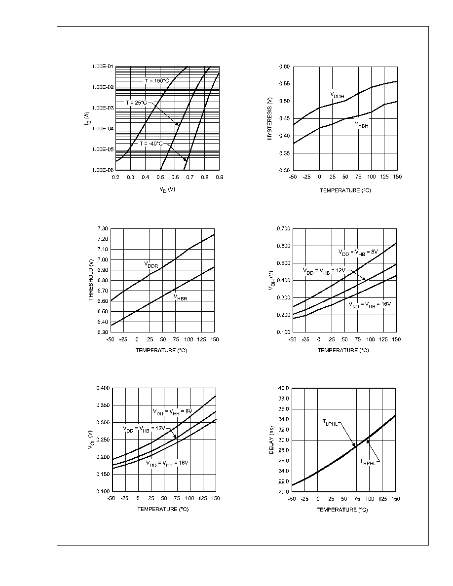
Typical Performance Characteristics
(Continued)
Diode Forward Voltage
Undervoltage Threshold Hysteresis vs Temperature
20088915
20088918
Undervoltage Rising Threshold vs Temperature
LO & HO Gate Drive -- High Level Output Voltage vs
Temperature
20088919
20088920
LO & HO Gate Drive -- Low Level Output Voltage vs
Temperature
Turn Off Propagation Delay vs Temperature
20088921
20088922
LM5102
www.national.com
6
Typical Performance Characteristics
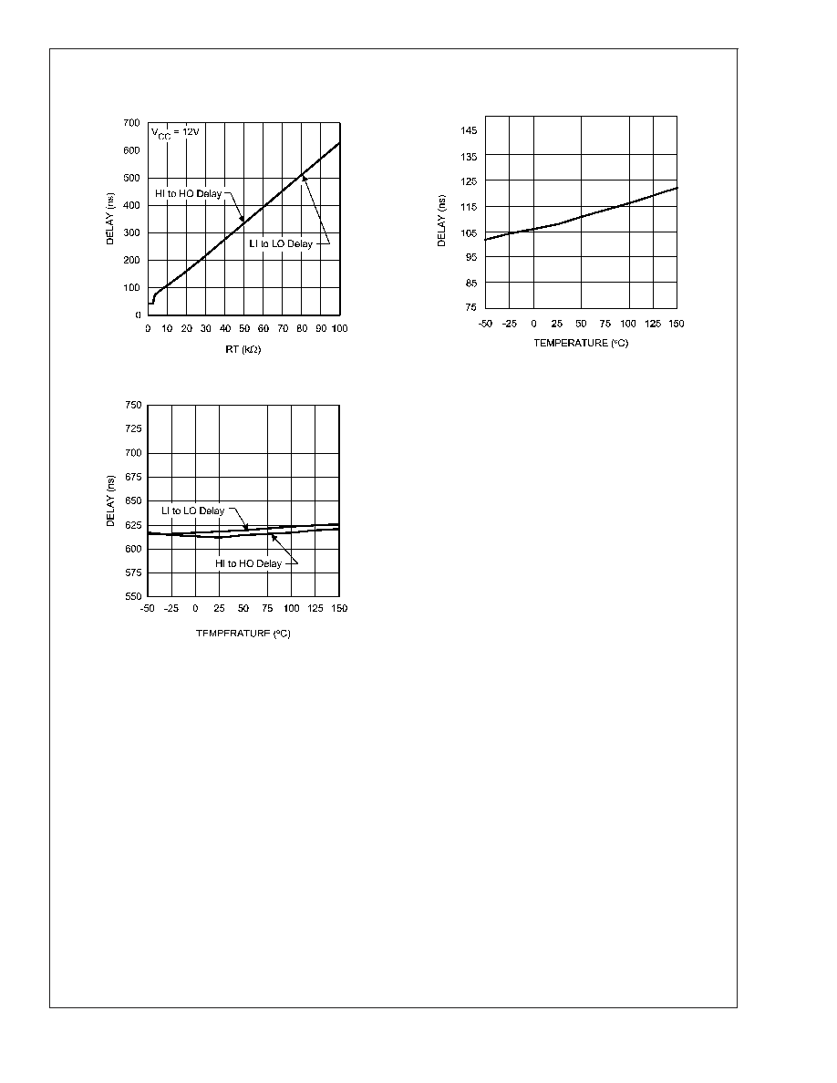
(Continued)
Turn On Delay vs RT Resistor Value
Turn On Delay vs Temperature (RT = 10k)
20088914
20088926
Turn On Delay vs Temperature (RT = 100k)
20088927
LM5102
www.national.com
7
LM5102 Waveforms
Operational Notes
The LM5102 offers a unique flexibility with independently
programmable delay of the rising edge for both high and low
side driver outputs independently. The delays are set with
resistors at the RT1 and RT2 pins, and can be adjusted from
100 ns to 600 ns. This feature reduces component count,
board space and cost compared to discrete solutions for
adjusting driver dead time. The wide delay programming
range provides the flexibility to optimize drive signal timing
for a wide range of MOSFETs and applications.
The RT pins are biased at 3V and current limited to 1 mA
maximum programming current. The time delay generator
will accommodate resistor values from 5k to 100k with
turn-on delay times that are proportional to the RT resis-
tance. In addition, each RT pin is monitored by a comparator
that will bypass the turn-on delay if the RT pin is pulled below
the timer elimination threshold (1.8V typical). Grounding the
RT pins programs the LM5102 to drive both outputs with
minimum turn-on delay.
STARTUP AND UVLO
Both top and bottom drivers include under-voltage lockout
(UVLO) protection circuitry which monitors the supply volt-
age (V
DD
) and bootstrap capacitor voltage (V
HB
≠ V
HS
)
independently. The UVLO circuit inhibits each driver until
sufficient supply voltage is available to turn-on the external
MOSFETs, and the built-in hysteresis prevents chattering
during supply voltage transitions. When the supply voltage is
applied to V
DD
pin of LM5102, the top and bottom gates are
20088903
(a)
20088904
(b)
FIGURE 3. Application Timing Waveforms
LM5102
www.national.com
8
Operational Notes
(Continued)
held low until V
DD
exceeds UVLO threshold, typically about
6.9V. Any UVLO condition on the bootstrap capacitor will
disable only the high side output (HO).
LAYOUT CONSIDERATIONS
The optimum performance of high and low side gate drivers
cannot be achieved without taking due considerations during
circuit board layout. Following points are emphasized.
1.
A low ESR/ESL capacitor must be connected close to
the IC, and between V
DD
and V
SS
pins and between HB
and HS pins to support high peak currents being drawn
from V
DD
during turn-on of the external MOSFET.
2.
To prevent large voltage transients at the drain of the top
MOSFET, a low ESR electrolytic capacitor must be con-
nected between MOSFET drain and ground (V
SS
).
3.
In order to avoid large negative transients on the switch
node (HS) pin, the parasitic inductances in the source of
top MOSFET and in the drain of the bottom MOSFET
(synchronous rectifier) must be minimized.
4.
Grounding considerations:
a) The first priority in designing grounding connections is
to confine the high peak currents from charging and
discharging the MOSFET gate in a minimal physical
area. This will decrease the loop inductance and mini-
mize noise issues on the gate terminal of the MOSFET.
The MOSFETs should be placed as close as possible to
the gate driver.
b) The second high current path includes the bootstrap
capacitor, the bootstrap diode, the local ground refer-
enced bypass capacitor and low side MOSFET body
diode. The bootstrap capacitor is recharged on the
cycle-by-cycle basis through the bootstrap diode from
the ground referenced V
DD
bypass capacitor. The re-
charging occurs in a short time interval and involves high
peak current. Minimizing this loop length and area on the
circuit board is important to ensure reliable operation.
5.
The resistors on the RT1 and RT2 timer pins must be
placed very close to the IC and seperated from high
current paths to avoid noise coupling to the time delay
generator which could disrupt timer operation.
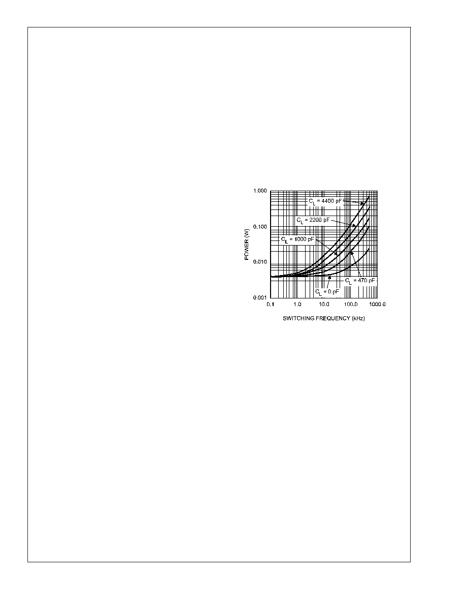
POWER DISSIPATION CONSIDERATIONS
The total IC power dissipation is the sum of the gate driver
losses and the bootstrap diode losses. The gate driver
losses are related to the switching frequency (f), output load
capacitance on LO and HO (C
L
), and supply voltage (V
DD
)
and can be roughly calculated as:
P
DGATES
= 2
∑
f
∑
C
L
∑
V
DD
2
There are some additional losses in the gate drivers due to
the internal CMOS stages used to buffer the LO and HO
outputs. The following plot shows the measured gate driver
power dissipation versus frequency and load capacitance. At
higher frequencies and load capacitance values, the power
dissipation is dominated by the power losses driving the
output loads and agrees well with the above equation. This
plot can be used to approximate the power losses due to the
gate drivers.
Gate Driver Power Dissipation (LO + HO)
V
CC
= 12V, Neglecting Diode Losses
20088905
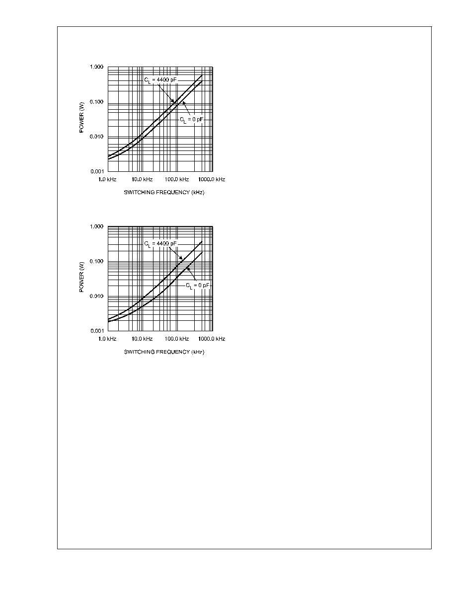
The bootstrap diode power loss is the sum of the forward
bias power loss that occurs while charging the bootstrap
capacitor and the reverse bias power loss that occurs during
reverse recovery. Since each of these events happens once
per cycle, the diode power loss is proportional to frequency.
Larger capacitive loads require more current to recharge the
bootstrap capacitor resulting in more losses. Higher input
voltages (V
IN
) to the half bridge result in higher reverse
recovery losses. The following plot was generated based on
calculations and lab measurements of the diode recovery
time and current under several operating conditions. This
can be useful for approximating the diode power dissipation.
LM5102
www.national.com
9
Operational Notes
(Continued)
Diode Power Dissipation V
IN
= 80V
20088906
Diode Power Dissipation V
IN
= 40V
20088907
The total IC power dissipation can be estimated from the
above plots by summing the gate drive losses with the
bootstrap diode losses for the intended application. Because
the diode losses can be significant, an external diode placed
in parallel with the internal bootstrap diode (refer to Figure 4)
and can be helpful in removing power from the IC. For this to
be effective, the external diode must be placed close to the
IC to minimize series inductance and have a significantly
lower forward voltage drop than the internal diode.
LM5102
www.national.com
10
Operational Notes
(Continued)
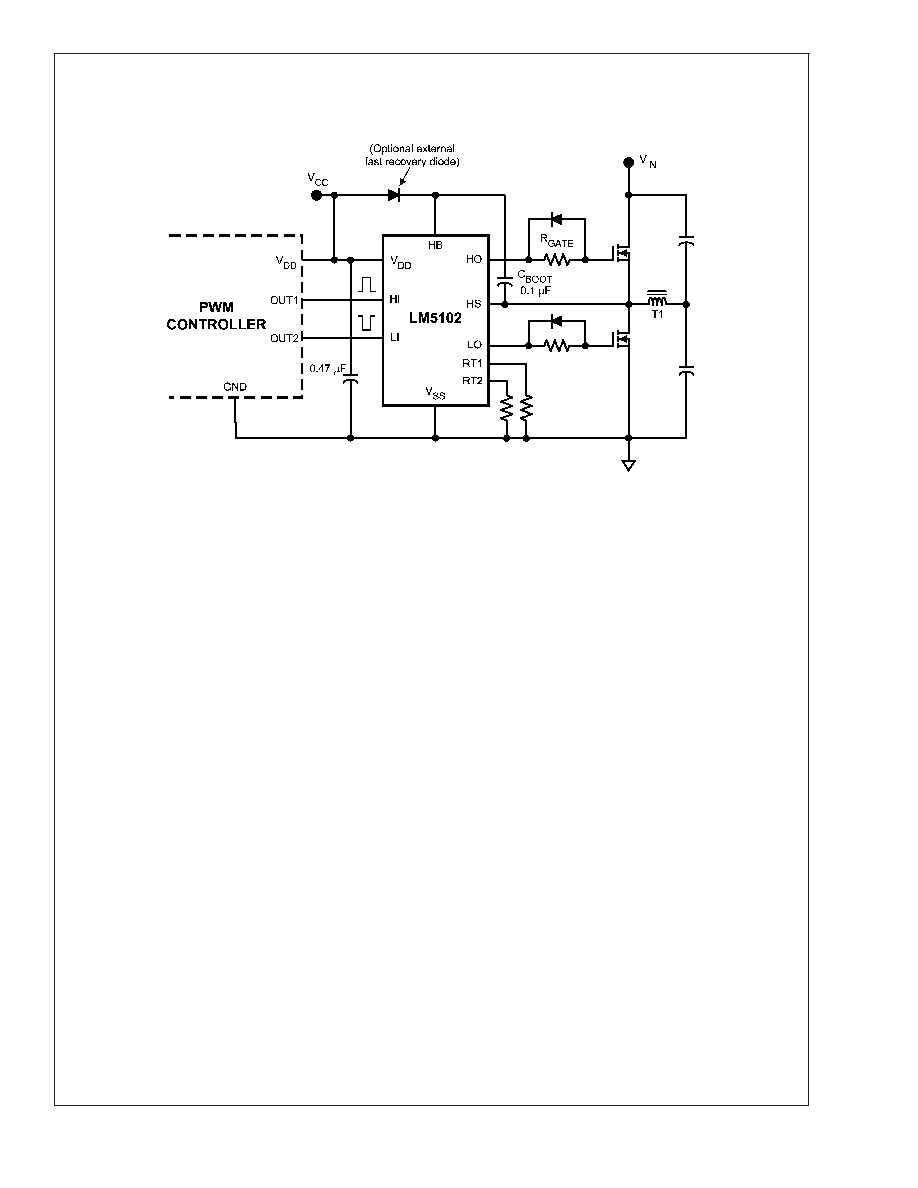
LM5102 Driving MOSFETs Connected in Half-Bridge Configuration
20088908
FIGURE 4.
LM5102
www.national.com
11
Physical Dimensions
inches (millimeters) unless otherwise noted
Notes: Unless otherwise specified
1.
Standard lead finish to be 200 microinches/5.00 micrometers minimum tin/lead (solder) on copper.
2.
Pin 1 identification to have half of full circle option.
3.
No JEDEC registration as of Feb. 2000.
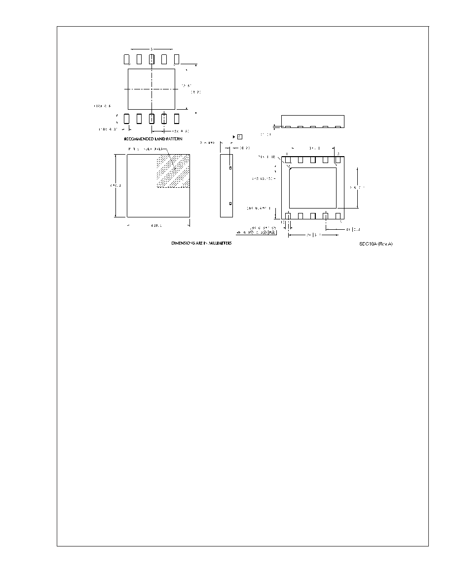
LLP-10 Outline Drawing
NS Package Number SDC10A
LM5102
www.national.com
12
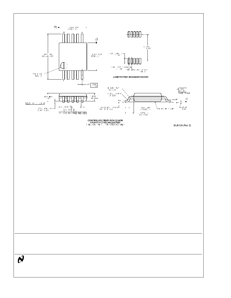
Physical Dimensions
inches (millimeters) unless otherwise noted (Continued)
Notes: Unless otherwise specified
1.
For solder thickness and composition, see "Solder Information" in the packaging section of the National Semiconductor web
page (www.national.com).
2.
Maximum allowable metal burr on lead tips at the package edges is 76 microns.
3.
No JEDEC registration as of May 2003.
MSOP-10 Outline Drawing
NS Package Number MUB10A
LIFE SUPPORT POLICY
NATIONAL'S PRODUCTS ARE NOT AUTHORIZED FOR USE AS CRITICAL COMPONENTS IN LIFE SUPPORT
DEVICES OR SYSTEMS WITHOUT THE EXPRESS WRITTEN APPROVAL OF THE PRESIDENT AND GENERAL
COUNSEL OF NATIONAL SEMICONDUCTOR CORPORATION. As used herein:
1. Life support devices or systems are devices or
systems which, (a) are intended for surgical implant
into the body, or (b) support or sustain life, and
whose failure to perform when properly used in
accordance with instructions for use provided in the
labeling, can be reasonably expected to result in a
significant injury to the user.
2. A critical component is any component of a life
support device or system whose failure to perform
can be reasonably expected to cause the failure of
the life support device or system, or to affect its
safety or effectiveness.
BANNED SUBSTANCE COMPLIANCE
National Semiconductor certifies that the products and packing materials meet the provisions of the Customer Products
Stewardship Specification (CSP-9-111C2) and the Banned Substances and Materials of Interest Specification
(CSP-9-111S2) and contain no ``Banned Substances'' as defined in CSP-9-111S2.
National Semiconductor
Americas Customer
Support Center
Email: new.feedback@nsc.com
Tel: 1-800-272-9959
National Semiconductor
Europe Customer Support Center
Fax: +49 (0) 180-530 85 86
Email: europe.support@nsc.com
Deutsch Tel: +49 (0) 69 9508 6208
English
Tel: +44 (0) 870 24 0 2171
FranÁais Tel: +33 (0) 1 41 91 8790
National Semiconductor
Asia Pacific Customer
Support Center
Email: ap.support@nsc.com
National Semiconductor
Japan Customer Support Center
Fax: 81-3-5639-7507
Email: jpn.feedback@nsc.com
Tel: 81-3-5639-7560
www.national.com
LM5102
High
V
oltage
Half-Bridge
Gate
Driver
with
Programmable
Delay
National does not assume any responsibility for use of any circuitry described, no circuit patent licenses are implied and National reserves the right at any time without notice to change said circuitry and specifications.