 | –≠–ª–µ–∫—Ç—Ä–æ–Ω–Ω—ã–π –∫–æ–º–ø–æ–Ω–µ–Ω—Ç: LM5106 | –°–∫–∞—á–∞—Ç—å:  PDF PDF  ZIP ZIP |
LM5106
100V Half Bridge Gate Driver with Programmable
Dead-Time
General Description
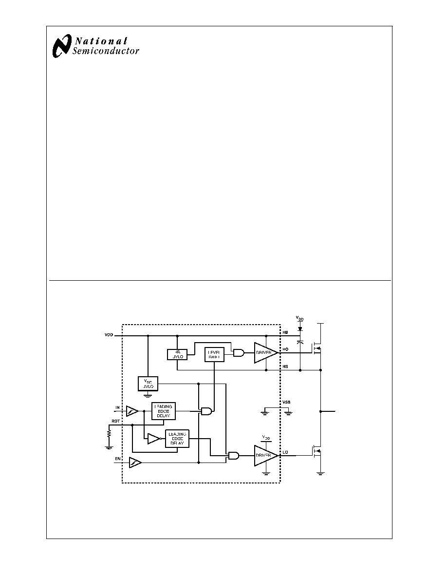
The LM5106 is a high voltage gate driver designed to drive
both the high side and low side N-Channel MOSFETs in a
synchronous buck or half bridge configuration. The floating
high side driver is capable of working with rail voltages up to
100V. The single control input is compatible with TTL signal
levels and a single external resistor programs the switching
transition dead-time through tightly matched turn-on delay
circuits. The robust level shift technology operates at high
speed while consuming low power and provides clean output
transitions. Under-voltage lockout disables the gate driver
when either the low side or the bootstrapped high side
supply voltage is below the operating threshold. The LM5106
is offered in the MSOP-10 or thermally enhanced 10-pin LLP
plastic package.
Features
n
Drives both a high side and low side N-channel
MOSFET
n
1.8A peak output sink current
n
1.2A peak output source current
n
Bootstrap supply voltage range up to 118V DC
n
Single TTL compatible Input
n
Programmable turn-on delays (Dead-time)
n
Enable Input pin
n
Fast turn-off propagation delays (32ns typical)
n
Drives 1000pF with 15ns rise and 10ns fall time
n
Supply rail under-voltage lockout
n
Low power consumption
Typical Applications
n
Solid State motor drives
n
Half and Full Bridge power converters
n
Two switch forward power converters
Package
n
LLP-10 (4 mm x 4 mm)
n
MSOP-10
Simplified Block Diagram
20175902
FIGURE 1.
January 2006
LM5106
100V
Half
Bridge
Gate
Driver
with
Programmable
Dead-T
ime
© 2006 National Semiconductor Corporation
DS201759
www.national.com
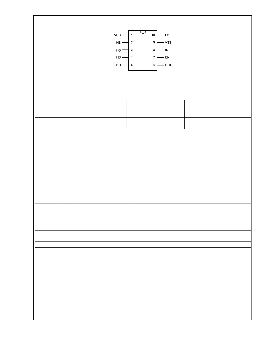
Connection Diagram
20175901
10-Lead MSOP or LLP
See NS Number MUB10A, SDC10A
Ordering Information
Ordering Number
Package Type
NSC Package Drawing
Supplied As
LM5106MM
MSOP-10
MUB10A
1000 shipped as Tape & Reel
LM5106MMX
MSOP-10
MUB10A
3500 shipped as Tape & Reel
LM5106SD
LLP-10
SDC10A
1000 shipped as Tape & Reel
LM5106SDX
LLP-10
SDC10A
4500 shipped as Tape & Reel
Pin Descriptions
Pin
Name
Description
Application Information
1
VDD
Positive gate drive supply
Decouple VDD to VSS using a low ESR/ESL capacitor, placed as
close to the IC as possible.
2
HB
High side gate driver
bootstrap rail
Connect the positive terminal of bootstrap capacitor to the HB pin
and connect negative terminal to HS. The Bootstrap capacitor
should be placed as close to IC as possible.
3
HO
High side gate driver
output
Connect to the gate of high side N-MOS device through a short,
low inductance path.
4
HS
High side MOSFET source
connection
Connect to the negative terminal of the bootststrap capacitor and to
the source of the high side N-MOS device.
5
NC
Not Connected
6
RDT
Dead-time programming
pin
A resistor from RDT to VSS programs the turn-on delay of both the
high and low side MOSFETs. The resistor should be placed close
to the IC to minimize noise coupling from adjacent PC board traces.
7
EN
Logic input for driver
Disable/Enable
TTL compatible threshold with hysteresis. LO and HO are held in
the low state when EN is low.
8
IN
Logic input for gate driver
TTL compatible threshold with hysteresis. The high side MOSFET
is turned on and the low side MOSFET turned off when IN is high.
9
VSS
Ground return
All signals are referenced to this ground.
10
LO
Low side gate driver output
Connect to the gate of the low side N-MOS device with a short, low
inductance path.
NA
EP
Exposed Pad
The exposed pad has no electrical contact. Connect to system
ground plane for reduced thermal resistance.
LM5106
www.national.com
2
Absolute Maximum Ratings
(Note 1)
If Military/Aerospace specified devices are required,
please contact the National Semiconductor Sales Office/
Distributors for availability and specifications.
V
DD
to V
SS
≠0.3V to +18V
HB to HS
≠0.3V to +18V
IN and EN to V
SS
≠0.3V to V
DD
+ 0.3V
LO to V
SS
≠0.3V to V
DD
+ 0.3V
HO to V
SS
HS ≠ 0.3V to HB + 0.3V
HS to V
SS
(Note 6)
-5V to +100V
HB to V
SS
118V
RDT to V
SS
≠0.3V to 5V
Junction Temperature
+150∞C
Storage Temperature Range
≠55∞C to +150∞C
ESD Rating HBM
(Note 2)
1.5 kV
Recommended Operating
Conditions
V
DD
+8V to +14V
HS (Note 6)
≠1V to 100V
HB
HS + 8V to HS + 14V
HS Slew Rate
<
50V/ns
Junction Temperature
≠40∞C to +125∞C
Electrical Characteristics
Specifications in standard typeface are for T
J
= +25∞C, and those in boldface
type apply over the full operating junction temperature range. Unless otherwise specified, V
DD
= HB = 12V, V
SS
= HS =
0V, EN = 5V. No load on LO or HO. RDT= 100k
(Note 4).
Symbol
Parameter
Conditions
Min
Typ
Max
Units
SUPPLY CURRENTS
I
DD
V
DD
Quiescent Current
IN = EN = 0V
0.34
0.6
mA
I
DDO
V
DD
Operating Current
f = 500 kHz
2.1
3.5
mA
I
HB
Total HB Quiescent Current
IN = EN = 0V
0.06
0.2
mA
I
HBO
Total HB Operating Current
f = 500 kHz
1.5
3
mA
I
HBS
HB to V
SS
Current, Quiescent
HS = HB = 100V
0.1
10
µA
I
HBSO
HB to V
SS
Current, Operating
f = 500 kHz
0.5
mA
INPUT IN and EN
V
IL
Low Level Input Voltage Threshold
0.8
1.8
V
V
IH
High Level Input Voltage Threshold
1.8
2.2
V
R
pd
Input Pulldown Resistance Pin IN and EN
100
200
500
k
DEAD-TIME CONTROLS
VRDT
Nominal Voltage at RDT
2.7
3
3.3
V
IRDT
RDT Pin Current Limit
RDT = 0V
0.75
1.5
2.25
mA
UNDER VOLTAGE PROTECTION
V
DDR
V
DD
Rising Threshold
6.2
6.9
7.6
V
V
DDH
V
DD
Threshold Hysteresis
0.5
V
V
HBR
HB Rising Threshold
5.9
6.6
7.3
V
V
HBH
HB Threshold Hysteresis
0.4
V
LO GATE DRIVER
V
OLL
Low-Level Output Voltage
I
LO
= 100 mA
0.21
0.4
V
V
OHL
High-Level Output Voltage
I
LO
= ≠100 mA,
V
OHL
= V
DD
≠ V
LO
0.5
0.85
V
I
OHL
Peak Pullup Current
LO = 0V
1.2
A
I
OLL
Peak Pulldown Current
LO = 12V
1.8
A
HO GATE DRIVER
V
OLH
Low-Level Output Voltage
I
HO
= 100 mA
0.21
0.4
V
V
OHH
High-Level Output Voltage
I
HO
= ≠100 mA,
V
OHH
= HB ≠ HO
0.5
0.85
V
I
OHH
Peak Pullup Current
HO = 0V
1.2
A
I
OLH
Peak Pulldown Current
HO = 12V
1.8
A
THERMAL RESISTANCE
JA
Junction to Ambient
(Note 3), (Note 5)
40
∞C/W
LM5106
www.national.com
3
Switching Characteristics
Specifications in standard typeface are for T
J
= +25∞C, and those in boldface
type apply over the full operating junction temperature range. Unless otherwise specified, V
DD
= HB = 12V, V
SS
= HS =
0V, No Load on LO or HO (Note 4).
Symbol
Parameter
Conditions
Min
Typ
Max
Units
t
LPHL
Lower Turn-Off Propagation Delay
32
56
ns
t
HPHL
Upper Turn-Off Propagation Delay
32
56
ns
t
LPLH
Lower Turn-On Propagation Delay
RDT = 100k
400
520
640
ns
t
HPLH
Upper Turn-On Propagation Delay
RDT = 100k
450
570
690
ns
t
LPLH
Lower Turn-On Propagation Delay
RDT = 10k
85
115
160
ns
t
HPLH
Upper Turn-On Propagation Delay
RDT = 10k
85
115
160
ns
t
en
, t
sd
Enable and Shutdown propagation delay
36
ns
DT1, DT2
Dead-time LO OFF to HO ON & HO OFF
to LO ON
RDT = 100k
510
µs
RDT = 10k
86
ns
MDT
Dead-time matching
RDT = 100k
50
ns
t
R
Either Output Rise Time
C
L
= 1000pF
15
ns
t
F
Either Output Fall Time
C
L
= 1000pF
10
ns
Note 1: Absolute Maximum Ratings indicate limits beyond which damage to the component may occur. Operating Ratings are conditions under which operation of
the device is guaranteed. Operating Ratings do not imply guaranteed performance limits. For guaranteed performance limits and associated test conditions, see the
Electrical Characteristics tables.
Note 2: The human body model is a 100 pF capacitor discharged through a 1.5k
resistor into each pin. Pin 2, Pin 3 and Pin 4 are rated at 500V.
Note 3: 4 layer board with Cu finished thickness 1.5/1.0/1.0/1.5 oz. Maximum die size used. 5x body length of Cu trace on PCB top. 50 x 50mm ground and power
planes embedded in PCB. See Application Note AN-1187.
Note 4: Min and Max limits are 100% production tested at 25∞C. Limits over the operating temperature range are guaranteed through correlation using Statistical
Quality Control (SQC) methods. Limits are used to calculate National's Average Outgoing Quality Level (AOQL).
Note 5: The
JA
is not a constant for the package and depends on the printed circuit board design and the operating conditions.
Note 6: In the application the HS node is clamped by the body diode of the external lower N-MOSFET, therefore the HS voltage will generally not exceed -1V.
However in some applications, board resistance and inductance may result in the HS node exceeding this stated voltage transiently.
If negative transients occur on HS, the HS voltage must never be more negative than V
DD
- 15V. For example, if V
DD
= 10V, the negative transients at HS must not
exceed -5V.
LM5106
www.national.com
4
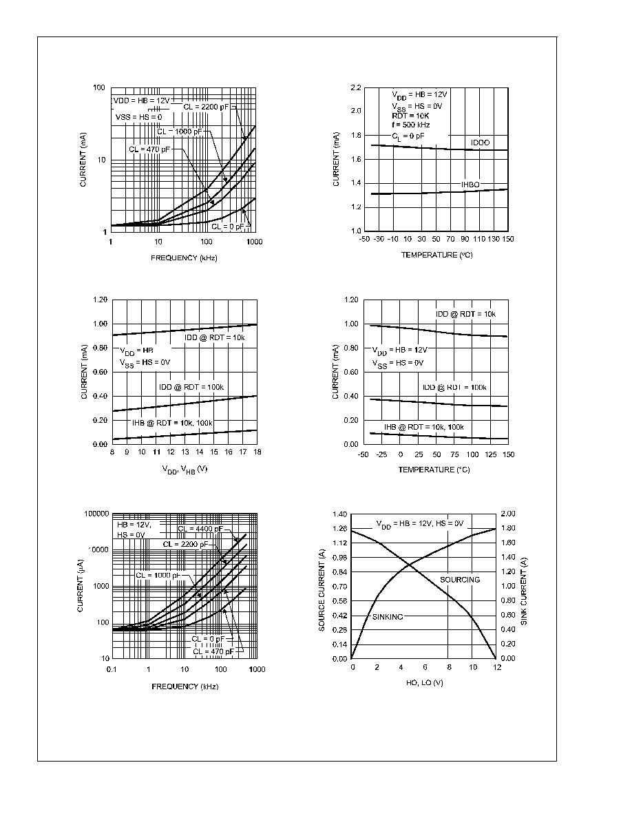
Typical Performance Characteristics
V
DD
Operating Current vs Frequency
Operating Current vs Temperature
20175910
20175911
Quiescent Current vs Supply Voltage
Quiescent Current vs Temperature
20175912
20175913
HB Operating Current vs Frequency
HO & LO Peak Output Current vs Output Voltage
20175916
20175917
LM5106
www.national.com
5