 | –≠–ª–µ–∫—Ç—Ä–æ–Ω–Ω—ã–π –∫–æ–º–ø–æ–Ω–µ–Ω—Ç: LM5109MAX | –°–∫–∞—á–∞—Ç—å:  PDF PDF  ZIP ZIP |
LM5109
100V / 1A Peak Half Bridge Gate Driver
General Description
The LM5109 is a low cost high voltage gate driver, designed
to drive both the high side and the low side N-Channel
MOSFETs in a synchronous buck or a half bridge configura-
tion. The floating high-side driver is capable of working with
rail voltages up to 100V. The outputs are independently
controlled with TTL compatible input thresholds. A robust
level shifter technology operates at high speed while con-
suming low power and providing clean level transitions from
the control input logic to the high side gate driver. Under-
voltage lockout is provided on both the low side and the high
side power rails. The device is available in the SOIC-8 and
the thermally enhanced LLP-8 packages.
Features
n
Drives both a high side and low side N-Channel
MOSFET
n
1A peak output current (1.0A sink / 1.0A source)
n
Independent TTL compatible inputs
n
Bootstrap supply voltage to 118V DC
n
Fast propagation times (27 ns typical)
n
Drives 1000 pF load with 15ns rise and fall times
n
Excellent propagation delay matching (2 ns typical)
n
Supply rail under-voltage lockout
n
Low power consumption
n
Pin compatible with ISL6700
Typical Applications
n
Current Fed push-pull converters
n
Half and Full Bridge power converters
n
Solid state motor drives
n
Two switch forward power converters
Package
n
SOIC-8
n
LLP-8 (4 mm x 4 mm)
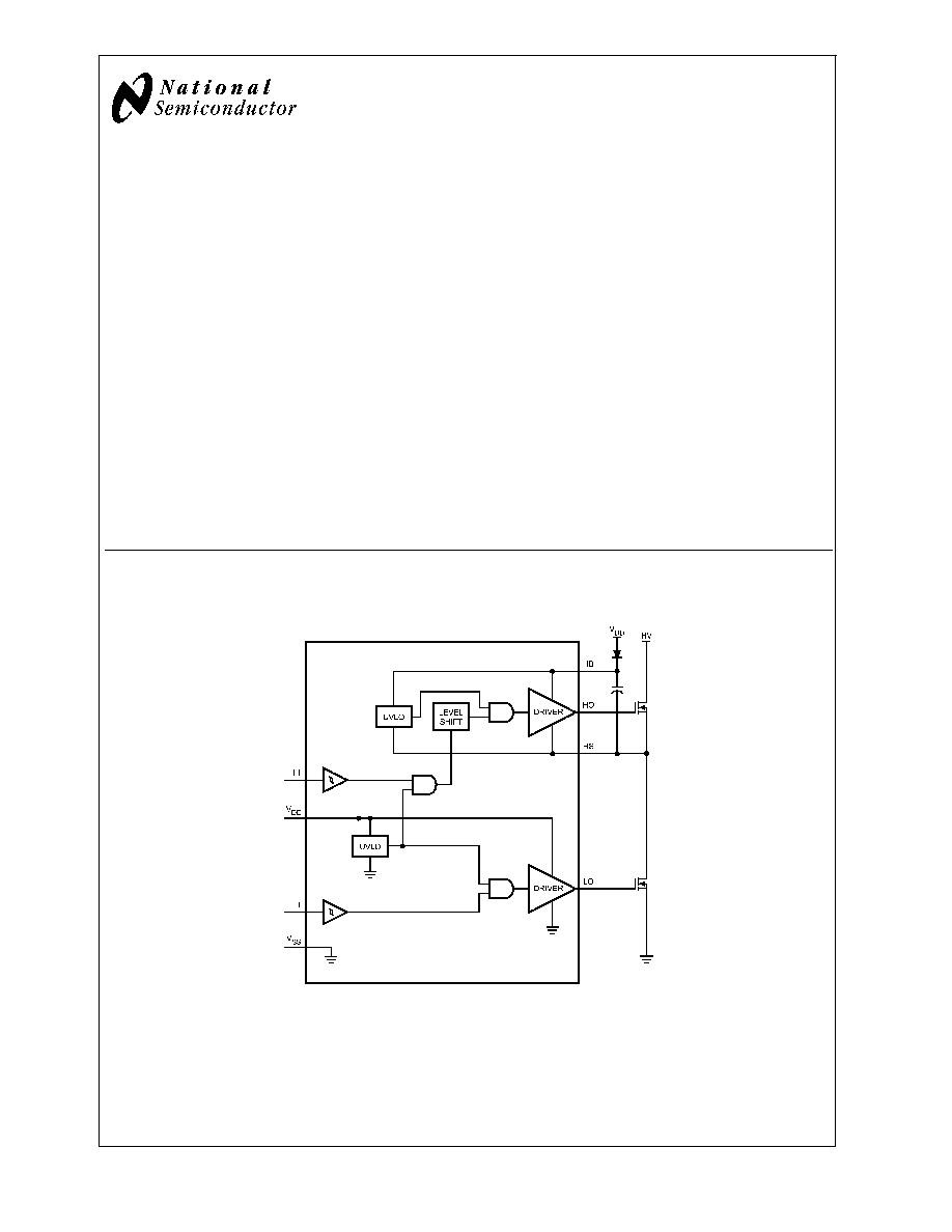
Simplified Block Diagram
20150501
FIGURE 1.
April 2005
LM5109
100V
/
1
A
Peak
Half
Bridge
Gate
Driver
© 2005 National Semiconductor Corporation
DS201505
www.national.com
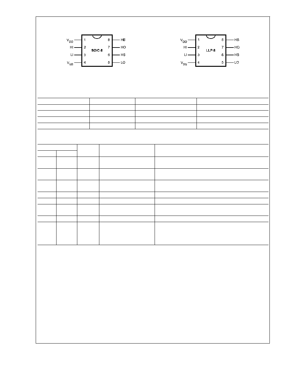
Connection Diagrams
Ordering Information
Ordering Number
Package Type
NSC Package Drawing
Supplied As
LM5109MA
SOIC-8
M08A
Shipped in anti static rails
LM5109MAX
SOIC-8
M08A
2500 shipped as Tape & Reel
LM5109SD
LLP-8
SDC08A
1000 shipped as Tape & Reel
LM5109SDX
LLP-8
SDC08A
4500 shipped as Tape & Reel
Pin Description
Pin #
Name
Description
Application Information
SO-8
LLP-8
1
1
V
DD
Positive gate drive supply
Locally decouple to V
SS
using low ESR/ESL capacitor located
as close to IC as possible.
2
2
HI
High side control input
The LM5109 HI input is compatible with TTL input thresholds.
Unused HI input should be tied to ground and not left open
3
3
LI
Low side control input
The LM5109 LI input is compatible with TTL input thresholds.
Unused LI input should be tied to ground and not left open.
4
4
V
SS
Ground reference
All signals are referenced to this ground.
5
5
LO
Low side gate driver output
Connect to the gate of the low side N-MOS device.
6
6
HS
High side source connection
Connect to the negative terminal of the bootstrap capacitor
and to the source of the high side N-MOS device.
7
7
HO
High side gate driver output
Connect to the gate of the low side N-MOS device.
8
8
HB
High side gate driver positive
supply rail
Connect the positive terminal of the bootstrap capacitor to HB
and the negative terminal of the bootstrap capacitor to HS.
The bootstrap capacitor should be placed as close to IC as
possible.
Note: For LLP-8 package it is recommended that the exposed pad on the bottom of the LM5109 be soldered to ground plane on the PCB board and the
ground plane should extend out from underneath the package to improve heat dissipation.
20150502
20150503
FIGURE 2.
LM5109
www.national.com
2
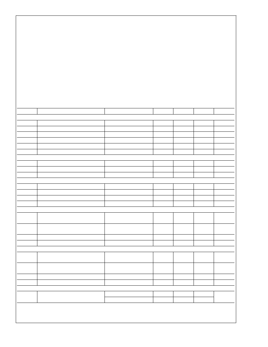
Absolute Maximum Ratings
(Note 1)
If Military/Aerospace specified devices are required,
please contact the National Semiconductor Sales Office/
Distributors for availability and specifications.
V
DD
to V
SS
-0.3V to 18V
HB to HS
-0.3V to 18V
LI or HI to V
SS
-0.3V to V
DD
+0.3V
LO to V
SS
-0.3V to V
DD
+0.3V
HO to V
SS
V
HS
-0.3V to V
HB
+0.3V
HS to V
SS
(Note 6)
-5V to 100V
HB to V
SS
118V
Junction Temperature
-40∞C to +150∞C
Storage Temperature Range
-55∞C to +150∞C
ESD Rating HBM (Note 2)
2 kV
Recommended Operating
Conditions
V
DD
8V to 14V
HS (Note 6)
-1V to 100V
HB
V
HS
+8V to V
HS
+14V
HS Slew Rate
<
50 V/ns
Junction Temperature
-40∞C to +125∞C
Electrical Characteristics
Specifications in standard typeface are for T
J
= +25∞C, and those in boldface type apply over the full operating junction tem-
perature range. Unless otherwise specified, V
DD
= V
HB
= 12V, V
SS
= V
HS
= 0V, No Load on LO or HO .
Symbol
Parameter
Conditions
Min
Typ
Max
Units
SUPPLY CURRENTS
I
DD
V
DD
Quiescent Current
LI = HI = 0V
0.3
0.6
mA
I
DDO
V
DD
Operating Current
f = 500 kHz
2.1
3.4
mA
I
HB
Total HB Quiescent Current
LI = HI = 0V
0.06
0.2
mA
I
HBO
Total HB Operating Current
f = 500 kHz
1.6
3.0
mA
I
HBS
HB to V
SS
Current, Quiescent
V
HS
= V
HB
= 100V
0.1
10
µA
I
HBSO
HB to V
SS
Current, Operating
f = 500 kHz
0.5
mA
INPUT PINS LI and HI
V
IL
Low Level Input Voltage Threshold
0.8
1.8
V
V
IH
High Level Input Voltage Threshold
1.8
2.2
V
R
I
Input Pulldown Resistance
100
180
500
k
UNDER VOLTAGE PROTECTION
V
DDR
V
DD
Rising Threshold
V
DDR
= V
DD
- V
SS
6.0
6.9
7.4
V
V
DDH
V
DD
Threshold Hysteresis
0.5
V
V
HBR
HB Rising Threshold
V
HBR
= V
HB
- V
HS
5.7
6.6
7.1
V
V
HBH
HB Threshold Hysteresis
0.4
V
LO GATE DRIVER
V
OLL
Low-Level Output Voltage
I
LO
= 100 mA
V
OHL
= V
LO
≠ V
SS
0.28
0.45
V
V
OHL
High-Level Output Voltage
I
LO
= -100 mA,
V
OHL
= V
DD
≠ V
LO
0.45
0.75
V
I
OHL
Peak Pullup Current
V
LO
= 0V
1.0
A
I
OLL
Peak Pulldown Current
V
LO
= 12V
1.0
A
HO GATE DRIVER
V
OLH
Low-Level Output Voltage
I
HO
= 100 mA
V
OLH
= V
HO
≠ V
HS
0.28
0.45
V
V
OHH
High-Level Output Voltage
I
HO
= -100 mA
V
OHH
= V
HB
≠ V
HO
0.45
0.75
V
I
OHH
Peak Pullup Current
V
HO
= 0V
1.0
A
I
OLH
Peak Pulldown Current
V
HO
= 12V
1.0
A
THERMAL RESISTANCE
JA
Junction to Ambient
SOIC-8
160
∞C/W
LLP-8 (Note 3)
40
LM5109
www.national.com
3
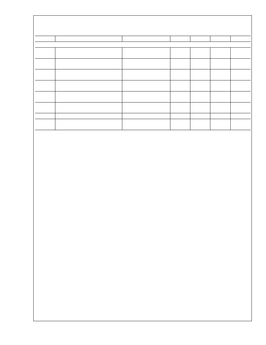
Switching Characteristics
Specifications in standard typeface are for T
J
= +25∞C, and those in boldface type apply over the full operating junction tem-
perature range. Unless otherwise specified, V
DD
= V
HB
= 12V, V
SS
= V
HS
= 0V, No Load on LO or HO.
Symbol
Parameter
Conditions
Min
Typ
Max
Units
LM5109
t
LPHL
Lower Turn-Off Propagation Delay (LI
Falling to LO Falling)
27
56
ns
t
HPHL
Upper Turn-Off Propagation Delay (HI
Falling to HO Falling)
27
56
ns
t
LPLH
Lower Turn-On Propagation Delay (LI
Rising to LO Rising)
29
56
ns
t
HPLH
Upper Turn-On Propagation Delay (HI
Rising to HO Rising)
29
56
ns
t
MON
Delay Matching: Lower Turn-On and
Upper Turn-Off
2
15
ns
t
MOFF
Delay Matching: Lower Turn-Off and
Upper Turn-On
2
15
ns
t
RC
, t
FC
Either Output Rise/Fall Time
C
L
= 1000 pF
15
-
ns
t
PW
Minimum Input Pulse Width that
Changes the Output
50
ns
Note 1: Absolute Maximum Ratings indicate limits beyond which damage to the component may occur. Operating Ratings are conditions under which operation of
the device is guaranteed. Operating Ratings do not imply guaranteed performance limits. For guaranteed performance limits and associated test conditions, see the
Electrical Characteristics tables.
Note 2: The human body model is a 100 pF capacitor discharged through a 1.5k
resistor into each pin. Pin 6 , Pin 7 and Pin 8 are rated at 500V.
Note 3: 4 layer board with Cu finished thickness 1.5/1/1/1.5 oz. Maximum die size used. 5x body length of Cu trace on PCB top. 50 x 50mm ground and power
planes embedded in PCB. See Application Note AN-1187.
Note 4: Min and Max limits are 100% production tested at 25∞C. Limits over the operating temperature range are guaranteed through correlation using Statistical
Quality Control (SQC) methods. Limits are used to calculate National's Average Outgoing Quality Level (AOQL).
Note 5: The
JA
is not a constant for the package and depends on the printed circuit board design and the operating conditions.
Note 6: In the application the HS node is clamped by the body diode of the external lower N-MOSFET, therefore the HS voltage will generally not exceed -1V.
However in some applications, board resistance and inductance may result in the HS node exceeding this stated voltage transiently.
If negative transients occur on HS, the HS voltage must never be more negative than V
DD
- 15V. For example, if V
DD
= 10V, the negative transients at HS must not
exceed -5V.
LM5109
www.national.com
4
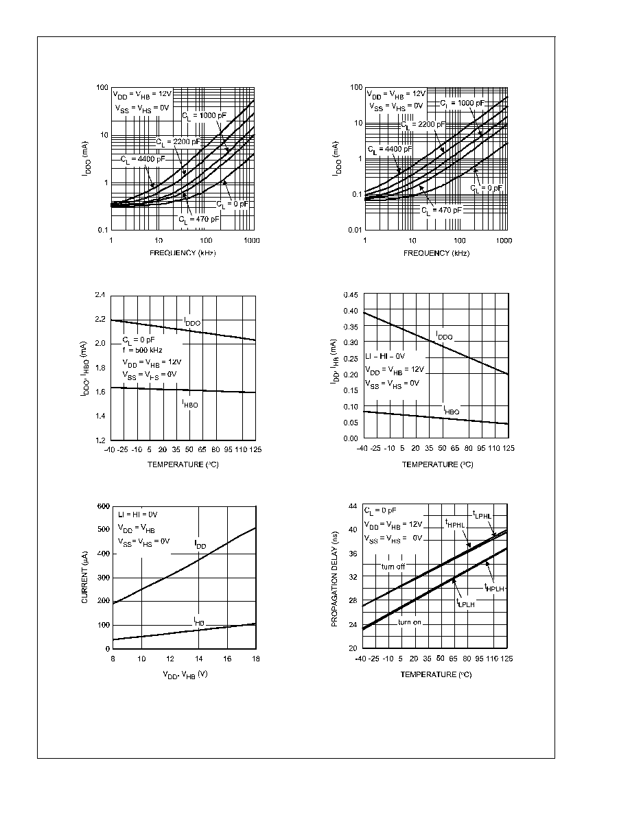
Typical performance Characteristics
V
DD
Operating Current vs Frequency
HB Operating Current vs Frequency
20150504
20150505
Operating Current vs Temperature
Quiescent Current vs Temperature
20150506
20150507
Quiescent Current vs Voltage
Propagation Delay vs Temperature
20150508
20150509
LM5109
www.national.com
5