LM5111
Dual 5A Compound Gate Driver
General Description
The LM5111 Dual Gate Driver replaces industry standard
gate drivers with improved peak output current and effi-
ciency. Each "compound" output driver stage includes MOS
and bipolar transistors operating in parallel that together sink
more than 5A peak from capacitive loads. Combining the
unique characteristics of MOS and bipolar devices reduces
drive current variation with voltage and temperature. Under-
voltage lockout protection is also provided. The drivers can
be operated in parallel with inputs and outputs connected to
double the drive current capability. This device is available in
the SOIC-8 package or the thermally enhanced MSOP8-EP
package.
Features
n
Independently drives two N-Channel MOSFETs
n
Compound CMOS and bipolar outputs reduce output
current variation
n
5A sink/3A source current capability
n
Two channels can be connected in parallel to double the
drive current
n
Independent inputs (TTL compatible)
n
Fast propagation times (25 ns typical)
n
Fast rise and fall times (14 ns/12 ns rise/fall with 2 nF
load)
n
Available in dual non-inverting, dual inverting and
combination configurations
n
Supply rail under-voltage lockout protection
n
Pin compatible with industry standard gate drivers
Typical Applications
n
Synchronous Rectifier Gate Drivers
n
Switch-mode Power Supply Gate Driver
n
Solenoid and Motor Drivers
Packages
n
SOIC-8
n
Thermally Enhanced MSOP8-EP
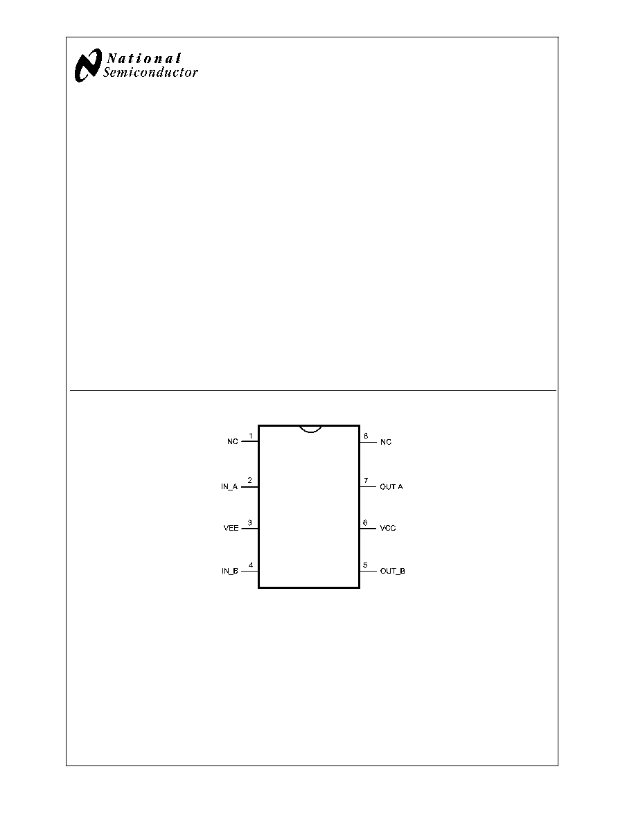
Connection Diagram
20112301
SOIC-8, eMSOP-8
March 2006
LM51
1
1
Dual
5A
Compound
Gate
Driver
© 2006 National Semiconductor Corporation
DS201123
www.national.com
Ordering Information
Order Number
Package Type
NSC Package Drawing
Supplied As
LM5111-1M
SOIC-8
M08A
Shipped in anti-static units, 95
Units/Rail
LM5111-1MX
SOIC-8
M08A
2500 shipped in Tape & Reel
LM5111-2M
SOIC-8
M08A
Shipped in anti-static units, 95
Units/Rail
LM5111-2MX
SOIC-8
M08A
2500 shipped in Tape & Reel
LM5111-3M
SOIC-8
M08A
Shipped in anti-static units, 95
Units/Rail
LM5111-3MX
SOIC-8
M08A
2500 shipped in Tape & Reel
LM5111-1MY
MSOP8-EP
MUY08A
1000 shipped in Tape & Reel
LM5111-1MYX
MSOP8-EP
MUY08A
3500 shipped in Tape & Reel
LM5111-2MY
MSOP8-EP
MUY08A
1000 shipped in Tape & Reel
LM5111-2MYX
MSOP8-EP
MUY08A
3500 shipped in Tape & Reel
LM5111-3MY
MSOP8-EP
MUY08A
1000 shipped in Tape & Reel
LM5111-3MYX
MSOP8-EP
MUY08A
3000 shipped in Tape & Reel
Pin Descriptions
Pin
Name
Description
Application Information
1
NC
No Connect
2
IN_A
`A' side control input
TTL compatible thresholds.
3
VEE
Ground reference for both inputs
and outputs
Connect to power ground.
4
IN_B
`B' side control input
TTL compatible thresholds.
5
OUT_B
Output for the `B' side driver.
Voltage swing of this output is from VCC to VEE.
The output stage is capable of sourcing 3A and
sinking 5A.
6
VCC
Positive output supply
Locally decouple to VEE
.
7
OUT_A.
Output for the `A' side driver.
Voltage swing of this output is from VCC to VEE.
The output stage is capable of sourcing 3A and
sinking 5A.
8
NC
No Connect
Configuration Table
Part Number
"A" Output Configuration
"B" Output Configuration
Package
LM5111-1M/-1MX/-1MY/-1MYX
Non-Inverting
Non-Inverting
SOIC-8, MSOP8-EP
LM5111-2M/-2MX/-2MY/-2MYX
Inverting
Inverting
SOIC-8, MSOP8-EP
LM5111-3M/-3MX/-3MY/-3MYX
Inverting
Non-Inverting
SOIC-8, MSOP8-EP
LM51
1
1
www.national.com
2
Absolute Maximum Ratings
(Note 1)
If Military/Aerospace specified devices are required,
please contact the National Semiconductor Sales Office/
Distributors for availability and specifications.
V
CC
to V
EE
-0.3V to 15V
IN to V
EE
-0.3V to 15V
Storage Temperature Range, (T
STG
)
-55∞C to +150∞C
Maximum Junction Temperature,
(T
J
(max))
+150∞C
Operating Junction Temperature
+125∞C
ESD Rating
2kV
Electrical Characteristics
T
J
= -40∞C to +125∞C, V
CC
= 12V, V
EE
= 0V, No Load on OUT_A or OUT_B, unless otherwise specified.
Symbol
Parameter
Conditions
Min
Typ
Max
Units
V
CC
Operating Range
V
CC
-V
EE
3.5
14
V
V
CCR
V
CC
Under Voltage Lockout
(rising)
V
CC
-V
EE
2.3
2.9
3.5
V
V
CCH
V
CC
Under Voltage Lockout
Hysteresis
230
mV
I
CC
V
CC
Supply Current (I
CC
)
IN_A = IN_B = 0V (5111-1)
1
2
mA
IN_A = IN_B = V
CC
(5111-2)
1
2
IN_A = V
CC
, IN_B = 0V (5111-3)
1
2
CONTROL INPUTS
V
IH
Logic High
2.2
V
V
IL
Logic Low
0.8
V
V
thH
High Threshold
1.3
1.75
2.2
V
V
thL
Low Threshold
0.8
1.35
2.0
V
HYS
Input Hysteresis
400
mV
I
IL
Input Current Low
IN_A=IN_B=V
CC
(5111-1-2-3)
-1
0.1
1
µA
I
IH
Input Current High
IN_B=V
CC
(5111-3)
10
18
25
IN_A=IN_B=V
CC
(5111-2)
-1
0.1
1
IN_A=IN_B=V
CC
(5111-1)
10
18
25
IN_A=V
CC
(5111-3)
-1
0.1
1
OUTPUT DRIVERS
R
OH
Output Resistance High
I
OUT
= -10 mA (Note 2)
30
50
R
OL
Output Resistance Low
I
OUT
= + 10 mA (Note 2)
1.4
2.5
I
Source
Peak Source Current
OUTA/OUTB = V
CC
/2,
200 ns Pulsed Current
3
A
I
Sink
Peak Sink Current
OUTA/OUTB = V
CC
/2,
200 ns Pulsed Current
5
A
LM51
1
1
www.national.com
3
Electrical Characteristics
(Continued)
T
J
= -40∞C to +125∞C, V
CC
= 12V, V
EE
= 0V, No Load on OUT_A or OUT_B, unless otherwise specified.
Symbol
Parameter
Conditions
Min
Typ
Max
Units
SWITCHING CHARACTERISTICS
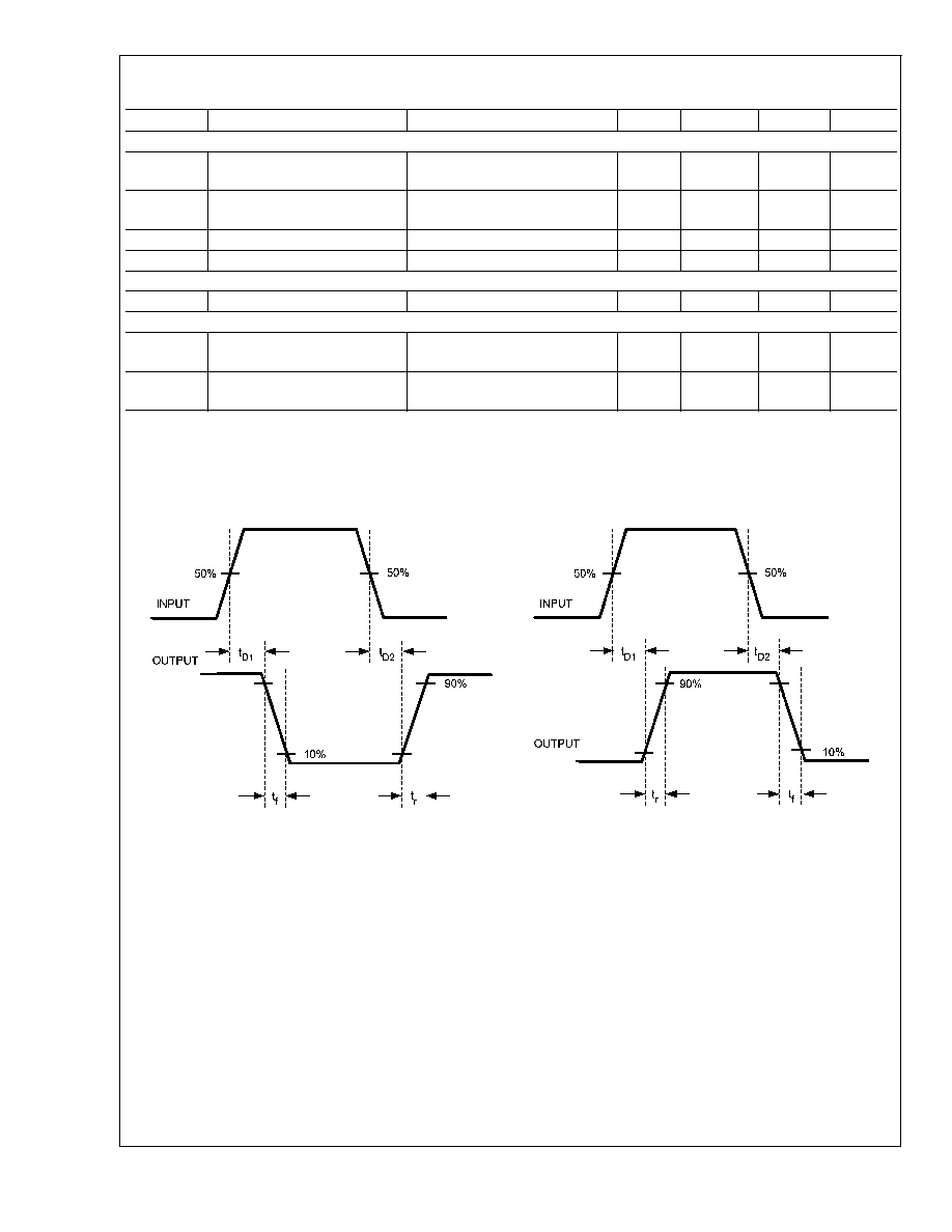
td1
Propagation Delay Time Low to
High, IN rising (IN to OUT)
C
LOAD
= 2 nF, see Figure 1
25
40
ns
td2
Propagation Delay Time High to
Low, IN falling (IN to OUT)
C
LOAD
= 2 nF, see Figure 1
25
40
ns
t
r
Rise Time
C
LOAD
= 2 nF, see Figure 1
14
25
ns
t
f
Fall Time
C
LOAD
= 2 nF, see Figure 1
12
25
ns
LATCHUP PROTECTION
AEC - Q100, Method 004
T
J
= 150∞C
500
mA
THERMAL RESISTANCE
JA
Junction to Ambient,
0 LFPM Air Flow
SOIC-8 Package
MSOP8-EP Package
170
60
∞C/W
JC
Junction to Case
SOIC-8 Package
MSOP8-EP Package
70
4.7
∞C/W
Note 1: Absolute Maximum Ratings are limits beyond which damage to the device may occur. Operating Ratings are conditions under which operation of the device
is intended to be functional. For guaranteed specifications and test conditions, see the Electrical Characteristics.
Note 2: The output resistance specification applies to the MOS device only. The total output current capability is the sum of the MOS and Bipolar devices.
Timing Waveforms
20112305
(a)
20112306
(b)
FIGURE 1. (a) Inverting, (b) Non-Inverting
LM51
1
1
www.national.com
4
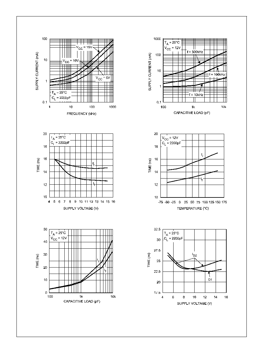
Typical Performance Characteristics
Supply Current vs Frequency
Supply Current vs Capacitive Load
20112310
20112311
Rise and Fall Time vs Supply Voltage
Rise and Fall Time vs Temperature
20112312
20112313
Rise and Fall Time vs Capacitive Load
Delay Time vs Supply Voltage
20112314
20112315
LM51
1
1
www.national.com
5