 | –≠–ª–µ–∫—Ç—Ä–æ–Ω–Ω—ã–π –∫–æ–º–ø–æ–Ω–µ–Ω—Ç: LM5112MYX | –°–∫–∞—á–∞—Ç—å:  PDF PDF  ZIP ZIP |
LM5112
Tiny 7A MOSFET Gate Driver
General Description
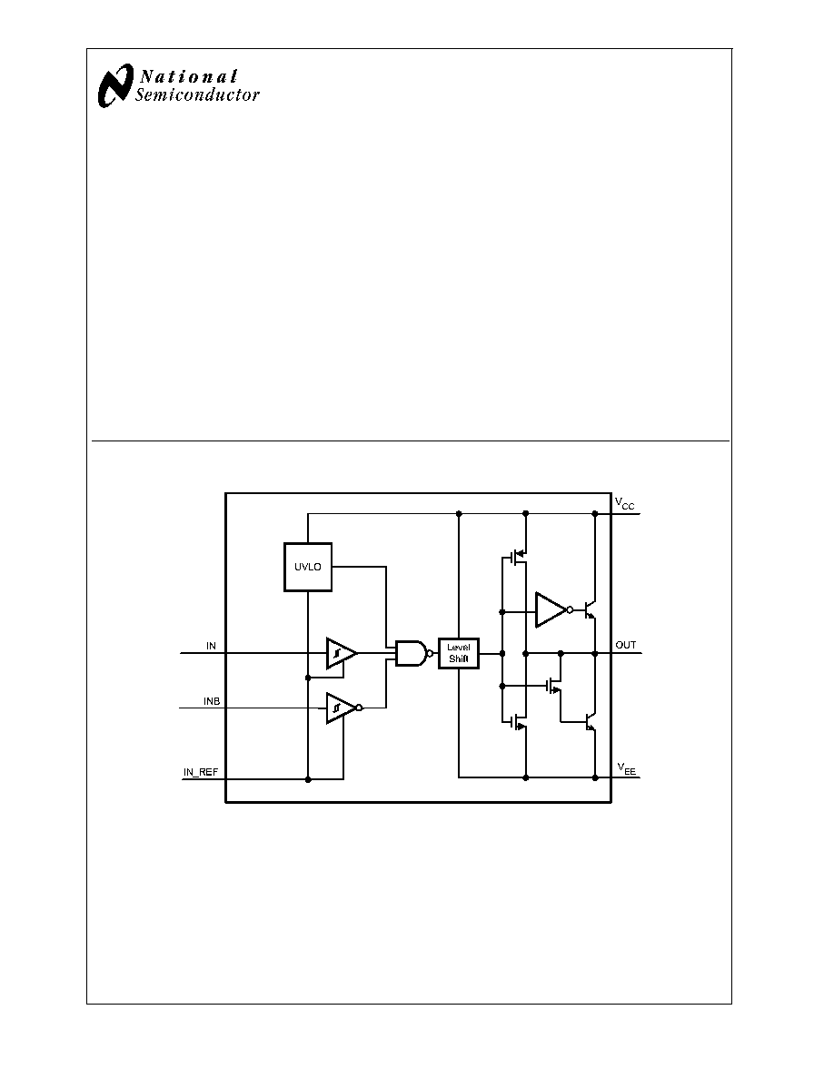
The LM5112 MOSFET gate driver provides high peak gate
drive current in the tiny LLP-6 package (SOT23 equivalent
footprint) or an 8-Lead exposed-pad MSOP package, with
improved power dissipation required for high frequency op-
eration. The compound output driver stage includes MOS
and bipolar transistors operating in parallel that together sink
more than 7A peak from capacitive loads. Combining the
unique characteristics of MOS and bipolar devices reduces
drive current variation with voltage and temperature. Under-
voltage lockout protection is provided to prevent damage to
the MOSFET due to insufficient gate turn-on voltage. The
LM5112 provides both inverting and non-inverting inputs to
satisfy requirements for inverting and non-inverting gate
drive with a single device type.
Features
n
Compound CMOS and bipolar outputs reduce output
current variation
n
7A sink/3A source current
n
Fast propagation times (25 ns typical)
n
Fast rise and fall times (14 ns/12 ns rise/fall with 2 nF
load)
n
Inverting and non-inverting inputs provide either
configuration with a single device
n
Supply rail under-voltage lockout protection
n
Dedicated input ground (IN_REF) for split supply or
single supply operation
n
Power Enhanced 6-pin LLP package (3.0mm x 3.0mm)
or thermally enhanced MSOP8-EP package
n
Output swings from V
CC
to V
EE
which can be negative
relative to input ground
Block Diagram
20066801
Block Diagram of LM5112
April 2006
LM51
12
T
iny
7A
MOSFET
Gate
Driver
© 2006 National Semiconductor Corporation
DS200668
www.national.com
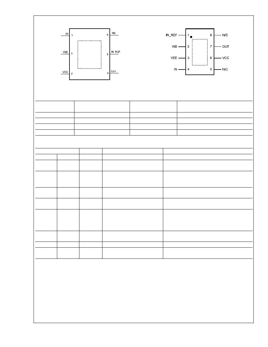
Pin Configurations
20066802
LLP-6
20066817
MSOP8-EP
Ordering Information
Order Number
Package Type
NSC Package
Drawing
Supplied As
LM5112MY
Exposed DAP MSOP8-EP
MUY08A
1000 shipped in Tape & Reel
LM5112MYX
Exposed DAP MSOP8-EP
MUY08A
3500 shipped in Tape & Reel
LM5112SD
LLP-6
SDE06A
1000 shipped in Tape & Reel
LM5112SDX
LLP-6
SDE06A
4500 shipped in Tape & Reel
Pin Descriptions
Pin
Name
Description
Application Information
LLP-6
MSOP-8
1
4
IN
Non-inverting input pin
TTL compatible thresholds. Pull up to VCC when
not used.
2
3
VEE
Power ground for driver outputs
Connect to either power ground or a negative
gate drive supply for positive or negative voltage
swing.
3
6
VCC
Positive Supply voltage input
Locally decouple to VEE. The decoupling
capacitor should be located close to the chip.
4
7
OUT
Gate drive output
Capable of sourcing 3A and sinking 7A. Voltage
swing of this output is from VEE to VCC.
5
1
IN_REF
Ground reference for control
inputs
Connect to power ground (VEE) for standard
positive only output voltage swing. Connect to
system logic ground when VEE is connected to a
negative gate drive supply.
6
2
INB
Inverting input pin
TTL compatible thresholds. Connect to IN_REF
when not used.
- - -
5, 8
N/C
Not internally connected
- - -
- - -
Exposed
Pad
Exposed Pad, underside of
package
Internally bonded to the die substrate. Connect to
VEE ground pin for low thermal impedance.
LM51
12
www.national.com
2
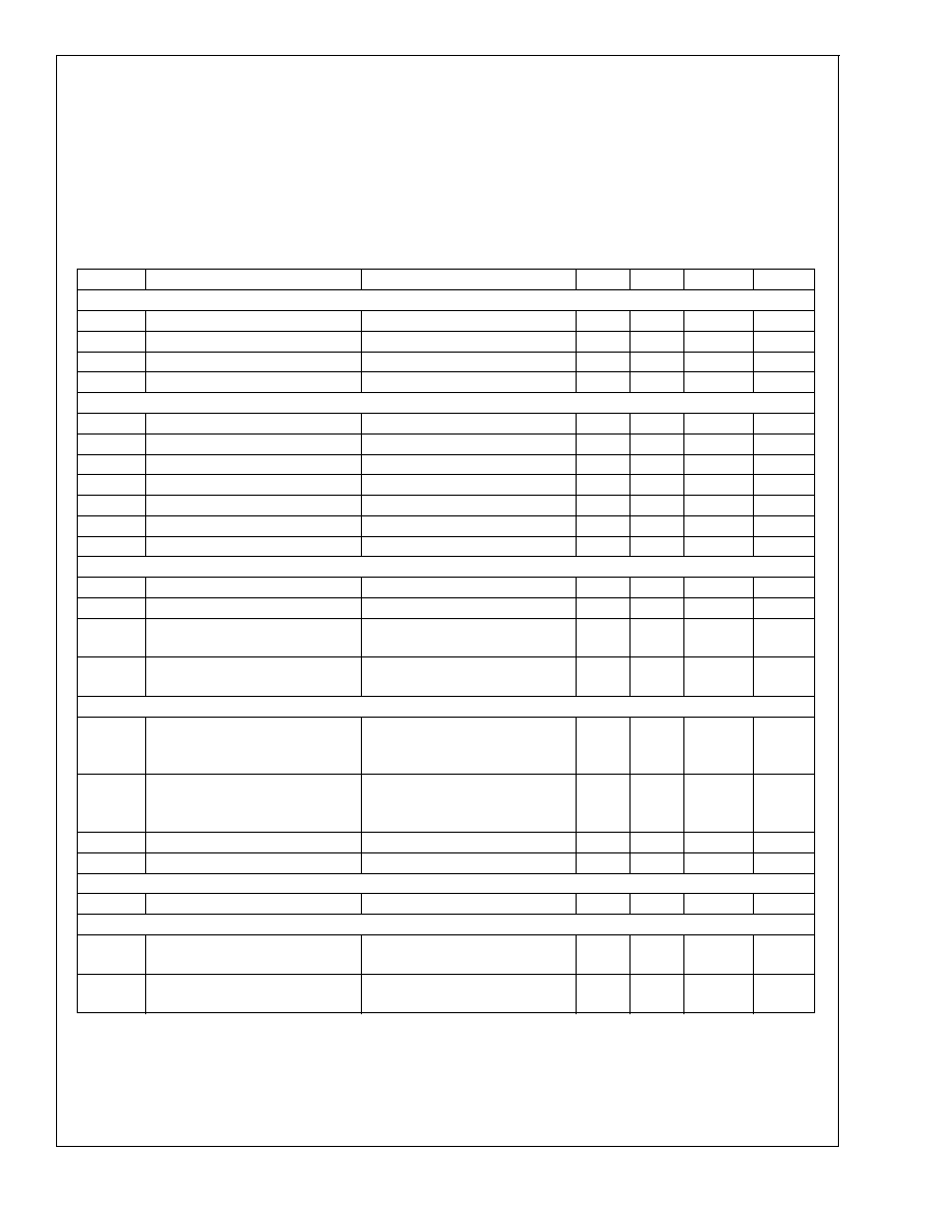
Absolute Maximum Ratings
(Note 1)
If Military/Aerospace specified devices are required,
please contact the National Semiconductor Sales Office/
Distributors for availability and specifications.
V
CC
to V
EE
-0.3V to 15V
V
CC
to IN_REF
-0.3V to 15V
IN/INB to IN_REF
-0.3V to 15V
IN_REF to V
EE
-0.3V to 5V
Storage Temperature Range
-55∞C to +150∞C
Maximum Junction Temperature
+150∞C
Operating Junction Temperature
-40∞C+125∞C
ESD Rating
2kV
Electrical Characteristics
T
J
= -40∞C to +125∞C, V
CC
= 12V, INB = IN_REF = V
EE
= 0V, No Load on out-
put, unless otherwise specified.
SYMBOL
PARAMETER
CONDITIONS
MIN
TYP
MAX
UNITS
SUPPLY
V
CC
V
CC
Operating Range
V
CC
≠ IN_REF and V
CC
- V
EE
3.5
14
V
UVLO
V
CC
Under-voltage Lockout (rising) V
CC
≠ IN_REF
2.4
3.0
3.5
V
V
CCH
V
CC
Under-voltage Hysteresis
230
mV
I
CC
V
CC
Supply Current
1.0
2.0
mA
CONTROL INPUTS
V
IH
Logic High
2.3
V
V
IL
Logic Low
0.8
V
V
thH
High Threshold
1.3
1.75
2.3
V
V
thL
Low Threshold
0.8
1.35
2.0
V
HYS
Input Hysteresis
400
mV
I
IL
Input Current Low
IN = INB = 0V
-1
0.1
1
µA
I
IH
Input Current High
IN = INB = V
CC
-1
0.1
1
µA
OUTPUT DRIVER
R
OH
Output Resistance High
I
OUT
= -10mA (Note 2)
30
50
R
OL
Output Resistance Low
I
OUT
= 10mA (Note 2)
1.4
2.5
I
SOURCE
Peak Source Current
OUT = V
CC
/2, 200ns pulsed
current
3
A
I
SINK
Peak Sink Current
OUT = V
CC
/2, 200ns pulsed
current
7
A
SWITCHING CHARACTERISTICS
td1
Propagation Delay Time Low to
High,
IN/ INB rising ( IN to OUT)
C
LOAD
= 2 nF, see Figure 1
25
40
ns
td2
Propagation Delay Time High to
Low,
IN / INB falling (IN to OUT)
C
LOAD
= 2 nF, see Figure 1
25
40
ns
tr
Rise time
C
LOAD
= 2 nF , see Figure 1
14
ns
tf
Fall time
C
LOAD
= 2 nF , see Figure 1
12
ns
LATCHUP PROTECTION
AEC ≠Q100, METHOD 004
T
J
= 150∞C
500
mA
THERMAL RESISTANCE
JA
Junction to Ambient,
0 LFPM Air Flow
LLP-6 Package
MSOP8-EP Package
40
60
∞C/W
JC
Junction to Case
LLP-6 Package
MSOP8-EP Package
7.5
4.7
∞C/W
Note 1: Absolute Maximum Ratings are limits beyond which damage to the device may occur. Operating Ratings are conditions under which operation of the device
is intended to be functional. For guaranteed specifications and test conditions, see the Electrical Characteristics.
Note 2: The output resistance specification applies to the MOS device only. The total output current capability is the sum of the MOS and Bipolar devices.
LM51
12
www.national.com
3
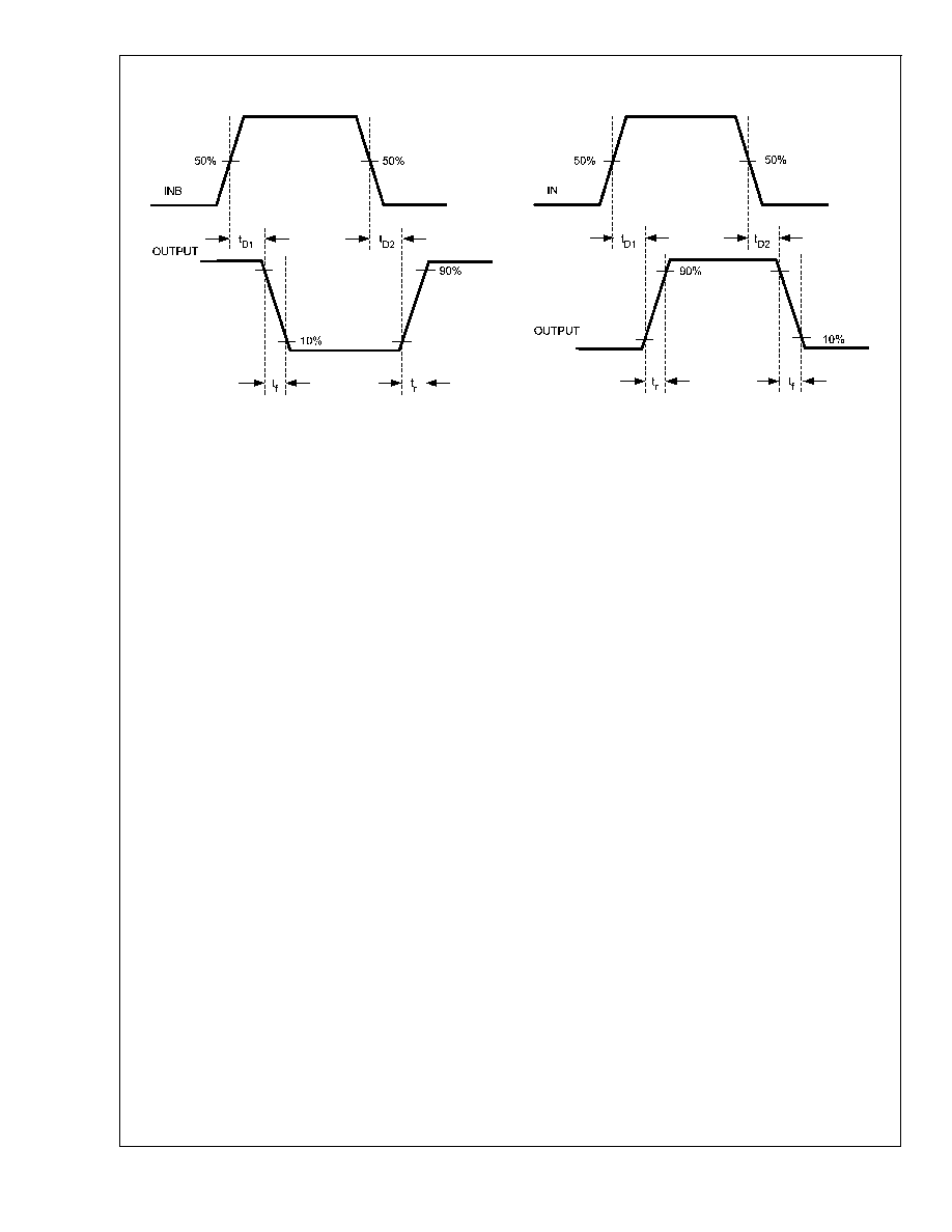
Timing Waveforms
20066804
(a)
20066805
(b)
FIGURE 1. (a) Inverting, (b) Non-Inverting
LM51
12
www.national.com
4
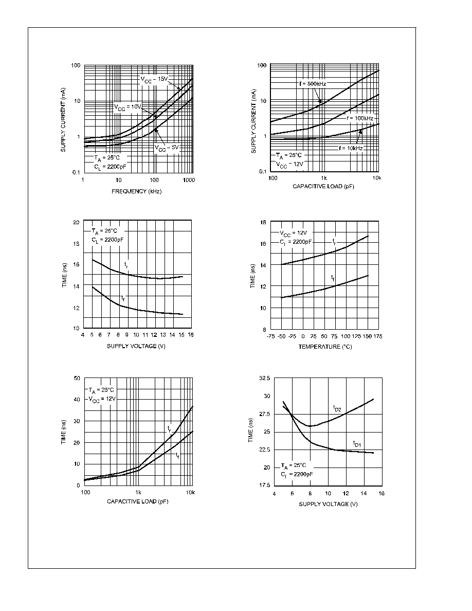
Typical Performance Characteristics
Supply Current vs Frequency
Supply Current vs Capacitive Load
20066807
20066808
Rise and Fall Time vs Supply Voltage
Rise and Fall Time vs Temperature
20066809
20066810
Rise and Fall Time vs Capacitive Load
Delay Time vs Supply Voltage
20066811
20066812
LM51
12
www.national.com
5