LM555
Timer
General Description
The LM555 is a highly stable device for generating accurate
time delays or oscillation. Additional terminals are provided
for triggering or resetting if desired. In the time delay mode of
operation, the time is precisely controlled by one external re-
sistor and capacitor. For astable operation as an oscillator,
the free running frequency and duty cycle are accurately
controlled with two external resistors and one capacitor. The
circuit may be triggered and reset on falling waveforms, and
the output circuit can source or sink up to 200mA or drive
TTL circuits.
Features
n
Direct replacement for SE555/NE555
n
Timing from microseconds through hours
n
Operates in both astable and monostable modes
n
Adjustable duty cycle
n
Output can source or sink 200 mA
n
Output and supply TTL compatible
n
Temperature stability better than 0.005% per ∞C
n
Normally on and normally off output
n
Available in 8-pin MSOP package
Applications
n
Precision timing
n
Pulse generation
n
Sequential timing
n
Time delay generation
n
Pulse width modulation
n
Pulse position modulation
n
Linear ramp generator
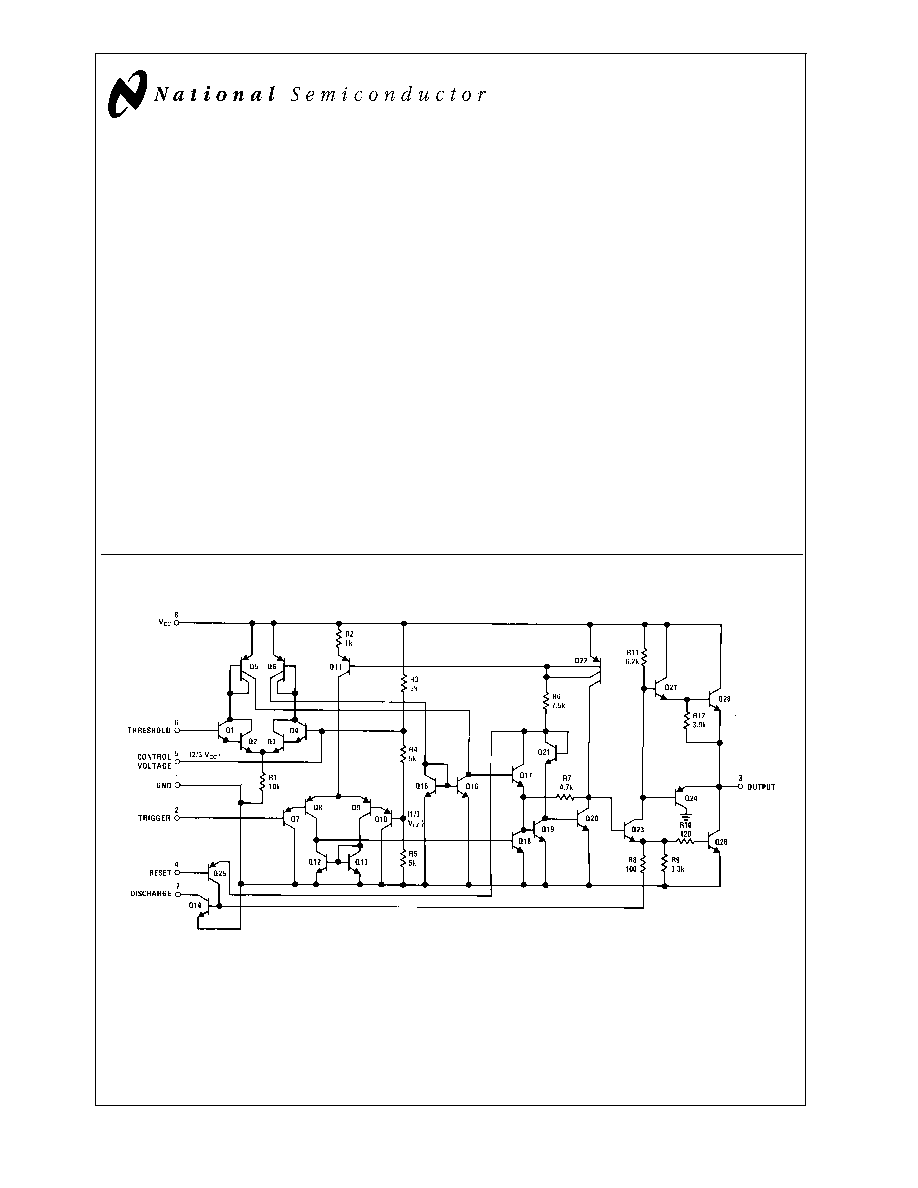
Schematic Diagram
DS007851-1
February 2000
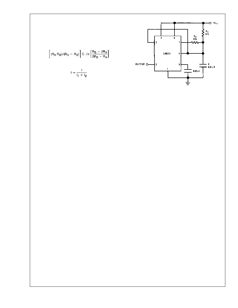
LM555
T
imer
© 2000 National Semiconductor Corporation
DS007851
www.national.com

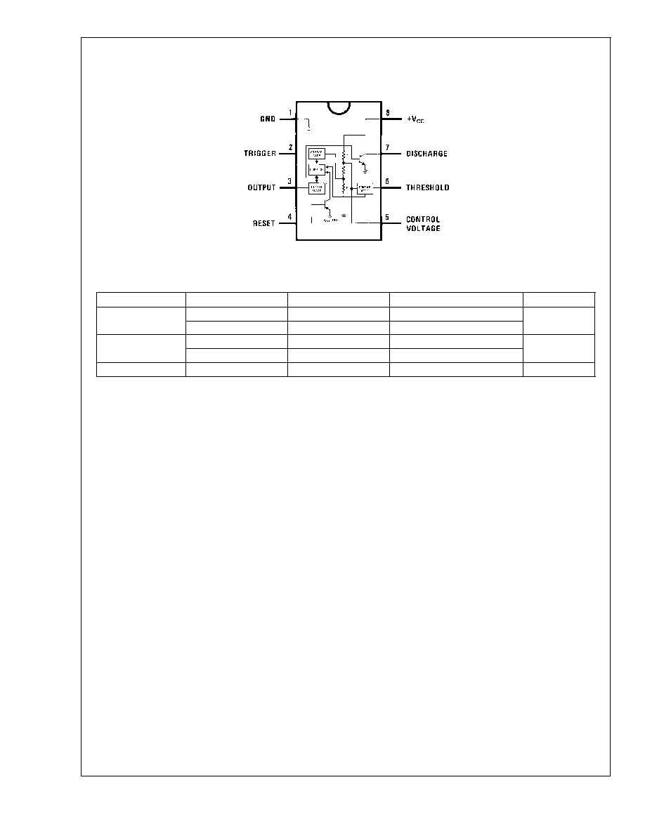
Connection Diagram
Ordering Information
Package
Part Number
Package Marking
Media Transport
NSC Drawing
8-Pin SOIC
LM555CM
LM555CM
Rails
M08A
LM555CMX
LM555CM
2.5k Units Tape and Reel
8-Pin MSOP
LM555CMM
Z55
1k Units Tape and Reel
MUA08A
LM555CMMX
Z55
3.5k Units Tape and Reel
8-Pin MDIP
LM555CN
LM555CN
Rails
N08E
Dual-In-Line, Small Outline
and Molded Mini Small Outline Packages
DS007851-3
Top View
LM555
www.national.com
2

Absolute Maximum Ratings
(Note 2)
If Military/Aerospace specified devices are required,
please contact the National Semiconductor Sales Office/
Distributors for availability and specifications.
Supply Voltage
+18V
Power Dissipation (Note 3)
LM555CM, LM555CN
1180 mW
LM555CMM
613 mW
Operating Temperature Ranges
LM555C
0∞C to +70∞C
Storage Temperature Range
-65∞C to +150∞C
Soldering Information
Dual-In-Line Package
Soldering (10 Seconds)
260∞C
Small Outline Packages
(SOIC and MSOP)
Vapor Phase (60 Seconds)
215∞C
Infrared (15 Seconds)
220∞C
See AN-450 "Surface Mounting Methods and Their Effect
on Product Reliability" for other methods of soldering
surface mount devices.
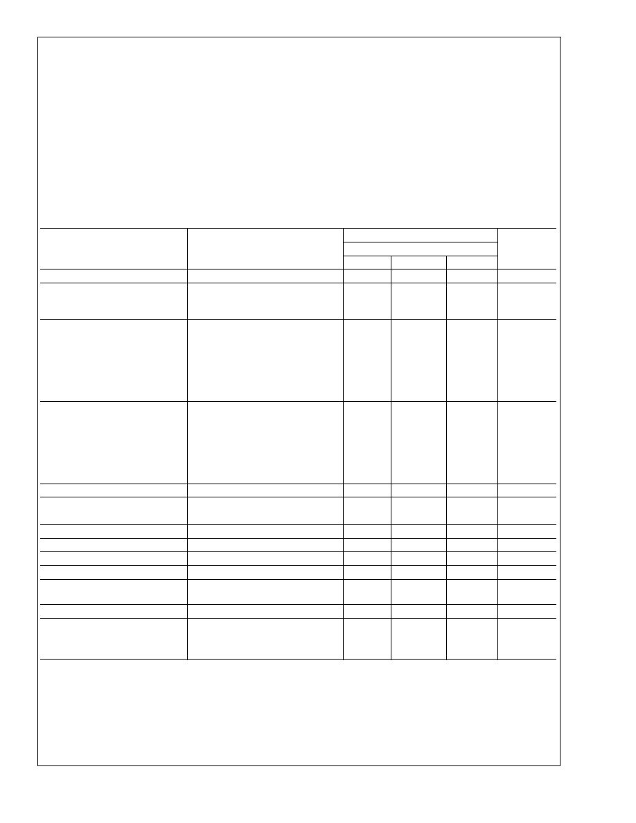
Electrical Characteristics
(Notes 1, 2)
(T
A
= 25∞C, V
CC
= +5V to +15V, unless othewise specified)
Parameter
Conditions
Limits
Units
LM555C
Min
Typ
Max
Supply Voltage
4.5
16
V
Supply Current
V
CC
= 5V, R
L
=
V
CC
= 15V, R
L
=
(Low State) (Note 4)
3
10
6
15
mA
Timing Error, Monostable
Initial Accuracy
1
%
Drift with Temperature
R
A
= 1k to 100k
,
50
ppm/∞C
C = 0.1µF, (Note 5)
Accuracy over Temperature
1.5
%
Drift with Supply
0.1
%/V
Timing Error, Astable
Initial Accuracy
2.25
%
Drift with Temperature
R
A
, R
B
= 1k to 100k
,
150
ppm/∞C
C = 0.1µF, (Note 5)
Accuracy over Temperature
3.0
%
Drift with Supply
0.30
%/V
Threshold Voltage
0.667
x V
CC
Trigger Voltage
V
CC
= 15V
5
V
V
CC
= 5V
1.67
V
Trigger Current
0.5
0.9
µA
Reset Voltage
0.4
0.5
1
V
Reset Current
0.1
0.4
mA
Threshold Current
(Note 6)
0.1
0.25
µA
Control Voltage Level
V
CC
= 15V
V
CC
= 5V
9
2.6
10
3.33
11
4
V
Pin 7 Leakage Output High
1
100
nA
Pin 7 Sat (Note 7)
Output Low
V
CC
= 15V, I
7
= 15mA
180
mV
Output Low
V
CC
= 4.5V, I
7
= 4.5mA
80
200
mV
LM555
www.national.com
3

Electrical Characteristics
(Notes 1, 2) (Continued)
(T
A
= 25∞C, V
CC
= +5V to +15V, unless othewise specified)
Parameter
Conditions
Limits
Units
LM555C
Min
Typ
Max
Output Voltage Drop (Low)
V
CC
= 15V
I
SINK
= 10mA
0.1
0.25
V
I
SINK
= 50mA
0.4
0.75
V
I
SINK
= 100mA
2
2.5
V
I
SINK
= 200mA
2.5
V
V
CC
= 5V
I
SINK
= 8mA
V
I
SINK
= 5mA
0.25
0.35
V
Output Voltage Drop (High)
I
SOURCE
= 200mA, V
CC
= 15V
12.5
V
I
SOURCE
= 100mA, V
CC
= 15V
12.75
13.3
V
V
CC
= 5V
2.75
3.3
V
Rise Time of Output
100
ns
Fall Time of Output
100
ns
Note 1: All voltages are measured with respect to the ground pin, unless otherwise specified.
Note 2: Absolute Maximum Ratings indicate limits beyond which damage to the device may occur. Operating Ratings indicate conditions for which the device is func-
tional, but do not guarantee specific performance limits. Electrical Characteristics state DC and AC electrical specifications under particular test conditions which guar-
antee specific performance limits. This assumes that the device is within the Operating Ratings. Specifications are not guaranteed for parameters where no limit is
given, however, the typical value is a good indication of device performance.
Note 3: For operating at elevated temperatures the device must be derated above 25∞C based on a +150∞C maximum junction temperature and a thermal resistance
of 106∞C/W (DIP), 170∞C/W (S0-8), and 204∞C/W (MSOP) junction to ambient.
Note 4: Supply current when output high typically 1 mA less at V
CC
= 5V.
Note 5: Tested at V
CC
= 5V and V
CC
= 15V.
Note 6: This will determine the maximum value of R
A
+ R
B
for 15V operation. The maximum total (R
A
+ R
B
) is 20M
.
Note 7: No protection against excessive pin 7 current is necessary providing the package dissipation rating will not be exceeded.
Note 8: Refer to RETS555X drawing of military LM555H and LM555J versions for specifications.
LM555
www.national.com
4

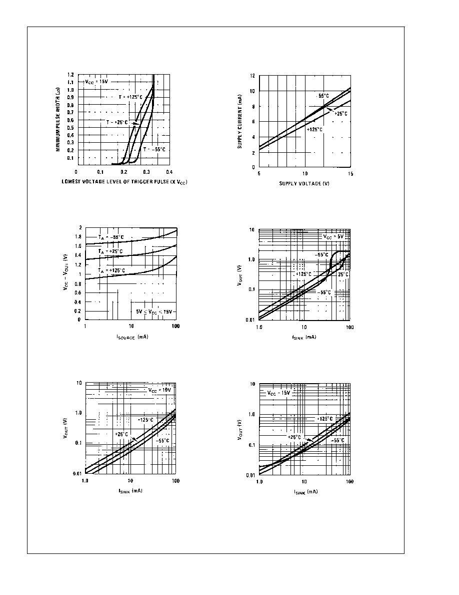
Typical Performance Characteristics
Minimuim Pulse Width
Required for Triggering
DS007851-4
Supply Current vs.
Supply Voltage
DS007851-19
High Output Voltage vs.
Output Source Current
DS007851-20
Low Output Voltage vs.
Output Sink Current
DS007851-21
Low Output Voltage vs.
Output Sink Current
DS007851-22
Low Output Voltage vs.
Output Sink Current
DS007851-23
LM555
www.national.com
5

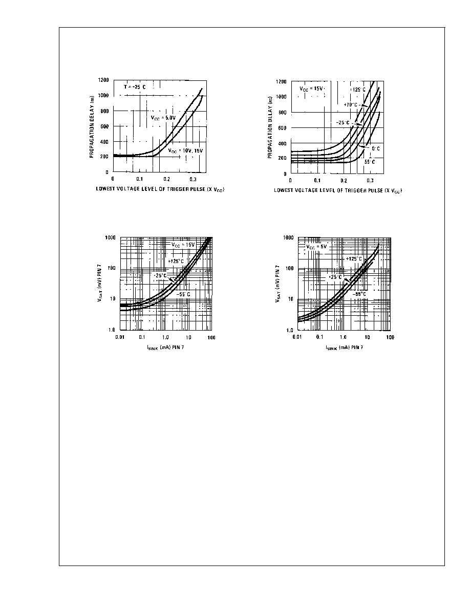
Typical Performance Characteristics
(Continued)
Output Propagation Delay vs.
Voltage Level of Trigger Pulse
DS007851-24
Output Propagation Delay vs.
Voltage Level of Trigger Pulse
DS007851-25
Discharge Transistor (Pin 7)
Voltage vs. Sink Current
DS007851-26
Discharge Transistor (Pin 7)
Voltage vs. Sink Current
DS007851-27
LM555
www.national.com
6

Applications Information
MONOSTABLE OPERATION
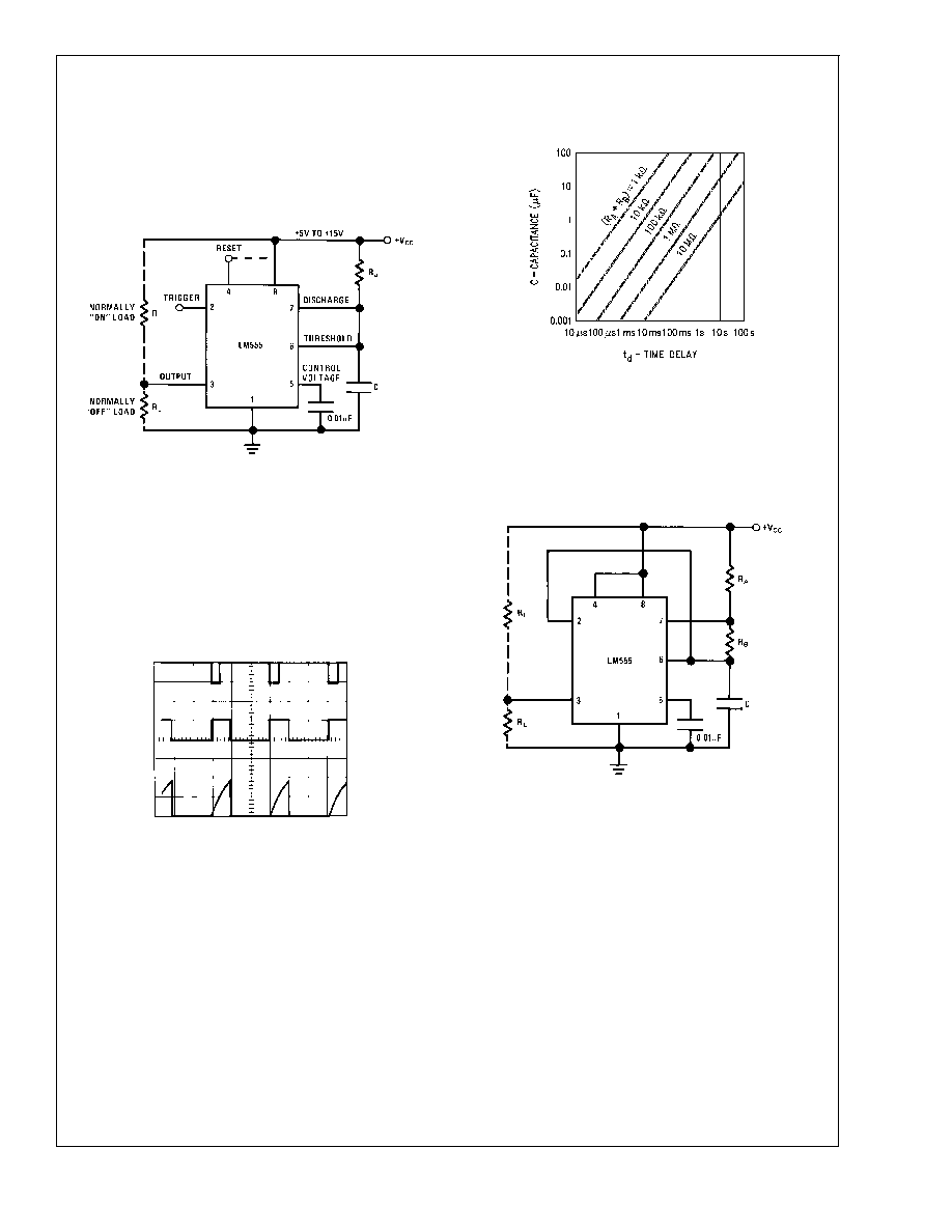
In this mode of operation, the timer functions as a one-shot
(
Figure 1). The external capacitor is initially held discharged
by a transistor inside the timer. Upon application of a nega-
tive trigger pulse of less than 1/3 V
CC
to pin 2, the flip-flop is
set which both releases the short circuit across the capacitor
and drives the output high.
The voltage across the capacitor then increases exponen-
tially for a period of t = 1.1 R
A
C, at the end of which time the
voltage equals 2/3 V
CC
. The comparator then resets the
flip-flop which in turn discharges the capacitor and drives the
output to its low state.
Figure 2 shows the waveforms gener-
ated in this mode of operation. Since the charge and the
threshold level of the comparator are both directly propor-
tional to supply voltage, the timing internal is independent of
supply.
During the timing cycle when the output is high, the further
application of a trigger pulse will not effect the circuit so long
as the trigger input is returned high at least 10µs before the
end of the timing interval. However the circuit can be reset
during this time by the application of a negative pulse to the
reset terminal (pin 4). The output will then remain in the low
state until a trigger pulse is again applied.
When the reset function is not in use, it is recommended that
it be connected to V
CC
to avoid any possibility of false trig-
gering.
Figure 3 is a nomograph for easy determination of R, C val-
ues for various time delays.
NOTE: In monostable operation, the trigger should be driven
high before the end of timing cycle.
ASTABLE OPERATION
If the circuit is connected as shown in
Figure 4 (pins 2 and 6
connected) it will trigger itself and free run as a multivibrator.
The external capacitor charges through R
A
+ R
B
and dis-
charges through R
B
. Thus the duty cycle may be precisely
set by the ratio of these two resistors.
In this mode of operation, the capacitor charges and dis-
charges between 1/3 V
CC
and 2/3 V
CC
. As in the triggered
mode, the charge and discharge times, and therefore the fre-
quency are independent of the supply voltage.
DS007851-5
FIGURE 1. Monostable
DS007851-6
V
CC
= 5V
Top Trace: Input 5V/Div.
TIME = 0.1 ms/DIV.
Middle Trace: Output 5V/Div.
R
A
= 9.1k
Bottom Trace: Capacitor Voltage 2V/Div.
C = 0.01µF
FIGURE 2. Monostable Waveforms
DS007851-7
FIGURE 3. Time Delay
DS007851-8
FIGURE 4. Astable
LM555
www.national.com
7

Applications Information
(Continued)
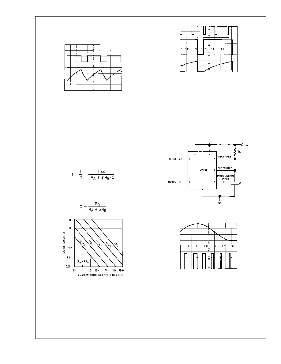
Figure 5 shows the waveforms generated in this mode of
operation.
The charge time (output high) is given by:
t
1
= 0.693 (R
A
+ R
B
) C
And the discharge time (output low) by:
t
2
= 0.693 (R
B
) C
Thus the total period is:
T = t
1
+ t
2
= 0.693 (R
A
+2R
B
) C
The frequency of oscillation is:
Figure 6 may be used for quick determination of these RC
values.
The duty cycle is:
FREQUENCY DIVIDER
The monostable circuit of
Figure 1 can be used as a fre-
quency divider by adjusting the length of the timing cycle.
Figure 7 shows the waveforms generated in a divide by three
circuit.
PULSE WIDTH MODULATOR
When the timer is connected in the monostable mode and
triggered with a continuous pulse train, the output pulse
width can be modulated by a signal applied to pin 5.
Figure
8 shows the circuit, and in Figure 9 are some waveform
examples.
DS007851-9
V
CC
= 5V
Top Trace: Output 5V/Div.
TIME = 20µs/DIV.
Bottom Trace: Capacitor Voltage 1V/Div.
R
A
= 3.9k
R
B
= 3k
C = 0.01µF
FIGURE 5. Astable Waveforms
DS007851-10
FIGURE 6. Free Running Frequency
DS007851-11
V
CC
= 5V
Top Trace: Input 4V/Div.
TIME = 20µs/DIV.
Middle Trace: Output 2V/Div.
R
A
= 9.1k
Bottom Trace: Capacitor 2V/Div.
C = 0.01µF
FIGURE 7. Frequency Divider
DS007851-12
FIGURE 8. Pulse Width Modulator
DS007851-13
V
CC
= 5V
Top Trace: Modulation 1V/Div.
TIME = 0.2 ms/DIV.
Bottom Trace: Output Voltage 2V/Div.
R
A
= 9.1k
C = 0.01µF
FIGURE 9. Pulse Width Modulator
LM555
www.national.com
8

Applications Information
(Continued)
PULSE POSITION MODULATOR
This application uses the timer connected for astable opera-
tion, as in
Figure 10, with a modulating signal again applied
to the control voltage terminal. The pulse position varies with
the modulating signal, since the threshold voltage and hence
the time delay is varied.
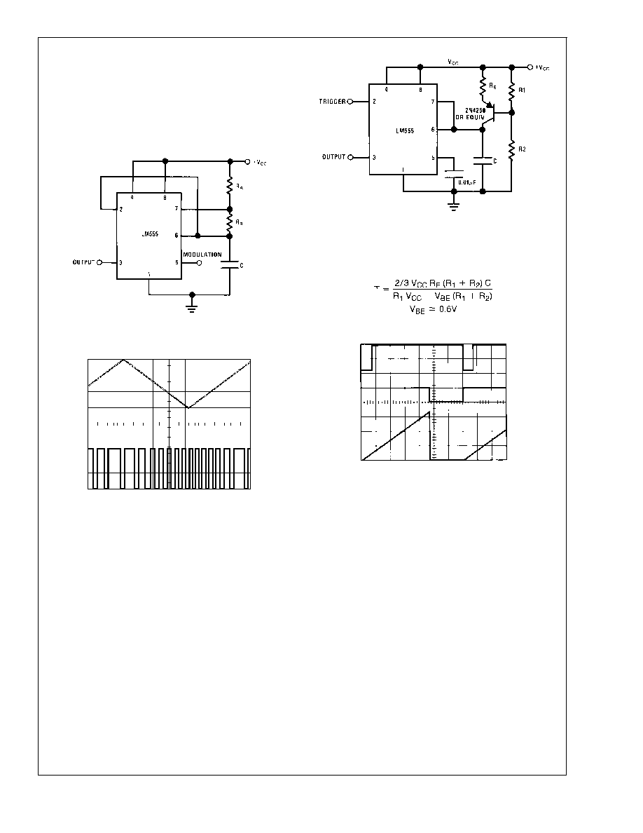
Figure 11 shows the waveforms
generated for a triangle wave modulation signal.
LINEAR RAMP
When the pullup resistor, R
A
, in the monostable circuit is re-
placed by a constant current source, a linear ramp is gener-
ated.
Figure 12 shows a circuit configuration that will perform
this function.
Figure 13 shows waveforms generated by the linear ramp.
The time interval is given by:
V
BE
.
0.6V
DS007851-14
FIGURE 10. Pulse Position Modulator
DS007851-15
V
CC
= 5V
Top Trace: Modulation Input 1V/Div.
TIME = 0.1 ms/DIV.
Bottom Trace: Output 2V/Div.
R
A
= 3.9k
R
B
= 3k
C = 0.01µF
FIGURE 11. Pulse Position Modulator
DS007851-16
FIGURE 12.
DS007851-17
V
CC
= 5V
Top Trace: Input 3V/Div.
TIME = 20µs/DIV.
Middle Trace: Output 5V/Div.
R
1
= 47k
Bottom Trace: Capacitor Voltage 1V/Div.
R
2
= 100k
R
E
= 2.7 k
C = 0.01 µF
FIGURE 13. Linear Ramp
LM555
www.national.com
9

Applications Information
(Continued)
50% DUTY CYCLE OSCILLATOR
For a 50% duty cycle, the resistors R
A
and R
B
may be con-
nected as in
Figure 14. The time period for the output high is
the same as previous, t
1
= 0.693 R
A
C. For the output low it
is t
2
=
Thus the frequency of oscillation is
Note that this circuit will not oscillate if R
B
is greater than 1/2
R
A
because the junction of R
A
and R
B
cannot bring pin 2
down to 1/3 V
CC
and trigger the lower comparator.
ADDITIONAL INFORMATION
Adequate power supply bypassing is necessary to protect
associated circuitry. Minimum recommended is 0.1µF in par-
allel with 1µF electrolytic.
Lower comparator storage time can be as long as 10µs
when pin 2 is driven fully to ground for triggering. This limits
the monostable pulse width to 10µs minimum.
Delay time reset to output is 0.47µs typical. Minimum reset
pulse width must be 0.3µs, typical.
Pin 7 current switches within 30ns of the output (pin 3) volt-
age.
DS007851-18
FIGURE 14. 50% Duty Cycle Oscillator
LM555
www.national.com
10

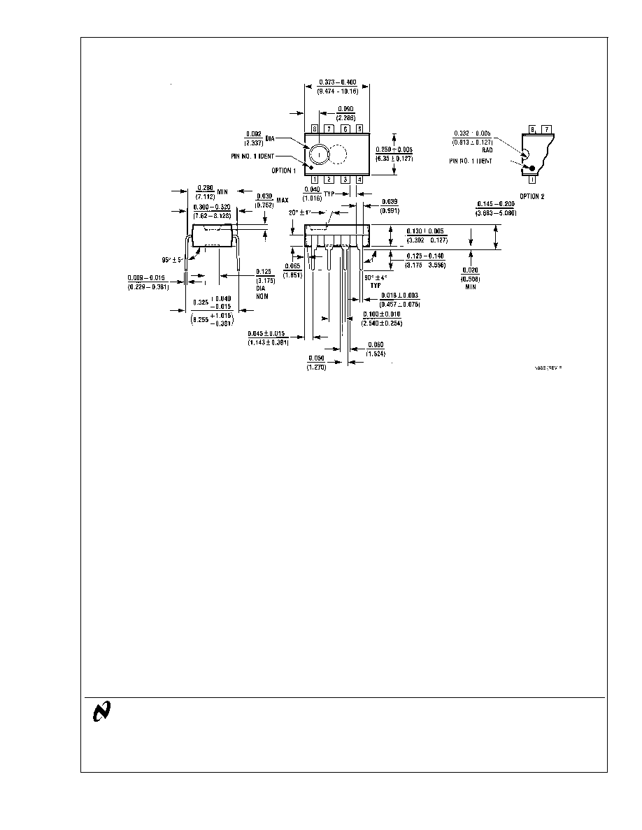
Physical Dimensions
inches (millimeters) unless otherwise noted
Small Outline Package (M)
NS Package Number M08A
8-Lead (0.118" Wide) Molded Mini Small Outline Package
NS Package Number MUA08A
LM555
www.national.com
11

Physical Dimensions
inches (millimeters) unless otherwise noted (Continued)
LIFE SUPPORT POLICY
NATIONAL'S PRODUCTS ARE NOT AUTHORIZED FOR USE AS CRITICAL COMPONENTS IN LIFE SUPPORT
DEVICES OR SYSTEMS WITHOUT THE EXPRESS WRITTEN APPROVAL OF THE PRESIDENT AND GENERAL
COUNSEL OF NATIONAL SEMICONDUCTOR CORPORATION. As used herein:
1. Life support devices or systems are devices or
systems which, (a) are intended for surgical implant
into the body, or (b) support or sustain life, and
whose failure to perform when properly used in
accordance with instructions for use provided in the
labeling, can be reasonably expected to result in a
significant injury to the user.
2. A critical component is any component of a life
support device or system whose failure to perform
can be reasonably expected to cause the failure of
the life support device or system, or to affect its
safety or effectiveness.
National Semiconductor
Corporation
Americas
Tel: 1-800-272-9959
Fax: 1-800-737-7018
Email: support@nsc.com
National Semiconductor
Europe
Fax: +49 (0) 180-530 85 86
Email: europe.support@nsc.com
Deutsch Tel: +49 (0) 69 9508 6208
English
Tel: +44 (0) 870 24 0 2171
FranÁais Tel: +33 (0) 1 41 91 8790
National Semiconductor
Asia Pacific Customer
Response Group
Tel: 65-2544466
Fax: 65-2504466
Email: ap.support@nsc.com
National Semiconductor
Japan Ltd.
Tel: 81-3-5639-7560
Fax: 81-3-5639-7507
www.national.com
Molded Dual-In-Line Package (N)
NS Package Number N08E
LM555
T
imer
National does not assume any responsibility for use of any circuitry described, no circuit patent licenses are implied and National reserves the right at any time without notice to change said circuitry and specifications.
