 | –≠–ª–µ–∫—Ç—Ä–æ–Ω–Ω—ã–π –∫–æ–º–ø–æ–Ω–µ–Ω—Ç: LM6035IBP | –°–∫–∞—á–∞—Ç—å:  PDF PDF  ZIP ZIP |
LMC6035/LMC6036
Low Power 2.7V Single Supply CMOS Operational
Amplifiers
General Description
The LMC6035/6 is an economical, low voltage op amp ca-
pable of rail-to-rail output swing into loads of 600
.
LMC6035 is available in a chip sized package (8-Bump
micro SMD) using National's micro SMD package technol-
ogy. Both allow for single supply operation and are guaran-
teed for 2.7V, 3V, 5V and 15V supply voltage. The 2.7 supply
voltage corresponds to the End-of-Life voltage (0.9V/cell) for
three NiCd or NiMH batteries in series, making the
LMC6035/6 well suited for portable and rechargeable sys-
tems. It also features a well behaved decrease in its speci-
fications at supply voltages below its guaranteed 2.7V op-
eration. This provides a "comfort zone" for adequate
operation at voltages significantly below 2.7V. Its ultra low
input currents (I
IN
) makes it well suited for low power active
filter application, because it allows the use of higher resistor
values and lower capacitor values. In addition, the drive
capability of the LMC6035/6 gives these op amps a broad
range of applications for low voltage systems.
Features
(Typical Unless Otherwise Noted)
n
LMC6035 in micro SMD Package
n
Guaranteed 2.7V, 3V, 5V and 15V Performance
n
Specified for 2 k
and 600 Loads
n
Wide Operating Range:
2.0V to 15.5V
n
Ultra Low Input Current:
20fA
n
Rail-to-Rail Output Swing
@
600
: 200mV from either rail at 2.7V
@
100k
: 5mV from either rail at 2.7V
n
High Voltage Gain:
126dB
n
Wide Input Common-Mode Voltage Range
-0.1V to 2.3V at V
S
= 2.7V
n
Low Distortion:
0.01% at 10kHz
n
LMC6035 Dual LMC6036 Quad
n
See AN-1112 for micro SMD considerations
Applications
n
Filters
n
High Impedance Buffer or Preamplifier
n
Battery Powered Electronics
n
Medical Instrumentation
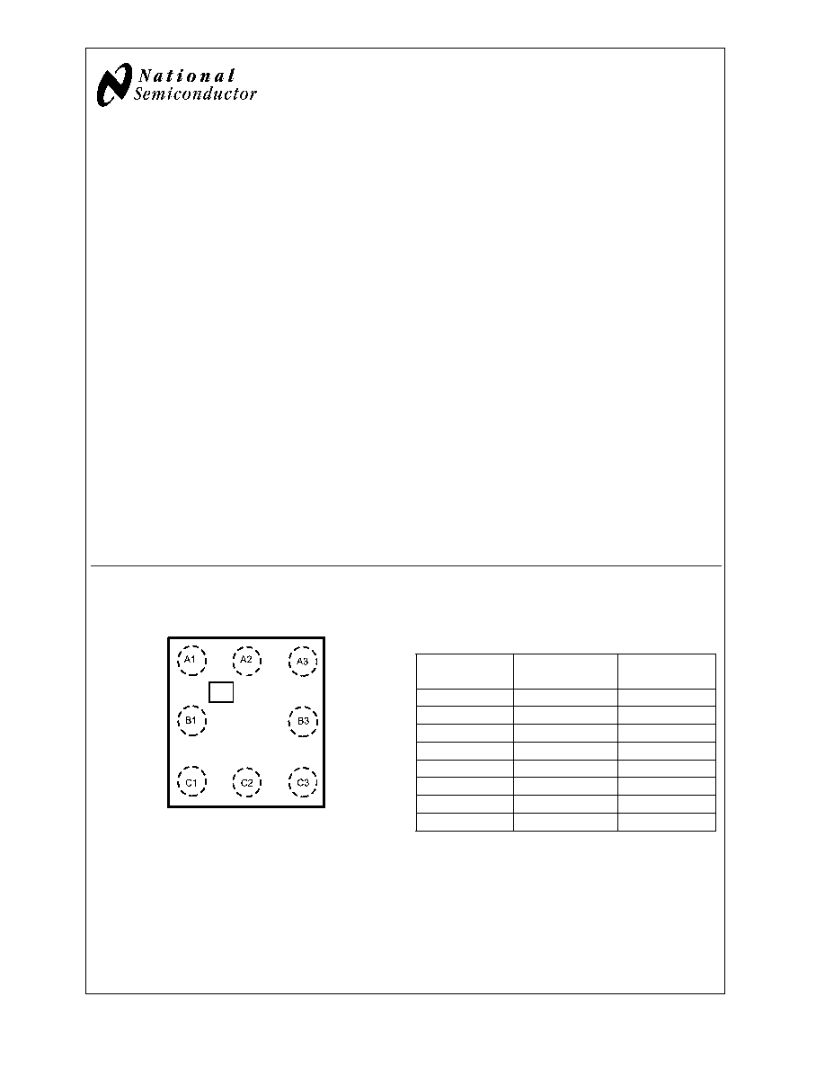
Connection Diagram
8-Bump microSMD
01283065
Top View
(Bump Side Down)
microSMD Connection Table
Bump Number
LM6035IBP
LMC6035IBPX
LMC6035ITL
LMC6035ITLX
A1
OUTPUT A
OUTPUT B
B1
IN A
-
V
+
C1
IN A
+
OUTPUT A
C2
V
-
IN A
-
C3
IN B
+
IN A
+
B3
IN B
-
V
-
A3
OUTPUT B
IN B
+
A2
V
+
IN B
-
October 2002
LMC6035/LMC6036
Low
Power
2.7V
Single
Supply
CMOS
Operational
Amplifiers
© 2002 National Semiconductor Corporation
DS012830
www.national.com
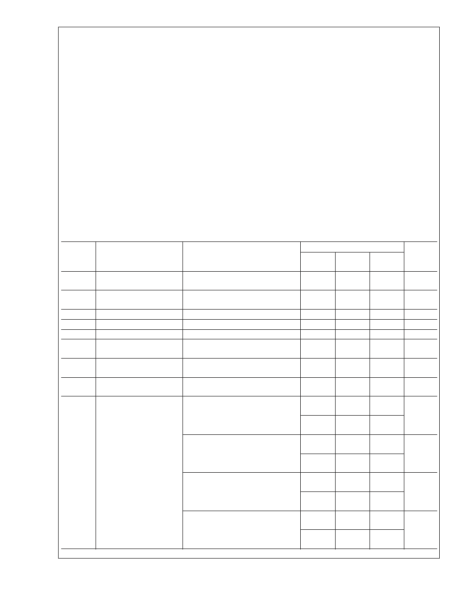
Absolute Maximum Ratings
(Note 1)
If Military/Aerospace specified devices are required,
please contact the National Semiconductor Sales Office/
Distributors for availability and specifications.
ESD Tolerance (Note 2)
Human Body Model
3000V
Machine Model
300V
Differential Input Voltage
±
Supply Voltage
Supply Voltage (V
+
- V
-
)
16V
Output Short Circuit to V
+
(Note 8)
Output Short Circuit to V
-
(Note 3)
Lead Temperature (soldering, 10
sec.)
260∞C
Current at Output Pin
±
18mA
Current at Input Pin
±
5mA
Current at Power Supply Pin
35mA
Storage Temperature Range
-65∞C to +150∞C
Junction Temperature (Note 4)
150∞C
Operating Ratings
(Note 1)
Supply Voltage
2.0V to 15.5V
Temperature Range
LMC6035I and LMC6036I
-40∞C
T
J
+85∞C
Thermal Resistance (
JA
)
8-pin MSOP
230∞C/W
8-pin SOIC
175∞C/W
14-pin SOIC
127∞C/W
14-pin TSSOP
137∞C/W
8-Bump (6 mil) micro SMD
220∞C/W
8-Bump (12 mil) Thin micro
SMD
220∞C/W
DC Electrical Characteristics
Unless otherwise specified, all limits guaranteed for T
J
= 25∞C, V
+
= 2.7V, V
-
= 0V, V
CM
= 1.0V, V
O
= 1.35V and R
L
>
1M
.
Boldface limits apply at the temperature extremes.
Symbol
Parameter
Conditions
LMC6035I/LMC6036I
Units
Min
(Note 6)
Typ
(Note 5)
Max
(Note 6)
V
OS
Input Offset Voltage
0.5
5
6
mV
TCV
OS
Input Offset Voltage
Average Drift
2.3
µV/∞C
I
IN
Input Current
(Note 11)
0.02
90
pA
I
OS
Input Offset Current
(Note 11)
0.01
45
PA
R
IN
Input Resistance
>
10
Tera
CMRR
Common Mode Rejection
Ratio
0.7V
V
CM
12.7V,
V
+
= 15V
63
60
96
dB
+PSRR
Positive Power Supply
Rejection Ratio
5V
V
+
15V,
V
O
= 2.5V
63
60
93
dB
-PSRR
Negative Power Supply
Rejection Ratio
0V
V
-
-10V,
V
O
= 2.5V, V
+
= 5V
74
70
97
dB
V
CM
Input Common-Mode
Voltage Range
V
+
= 2.7V
For CMRR
40dB
-0.1
0.3
0.5
V
2.0
1.7
2.3
V
+
= 3V
For CMRR
40dB
-0.3
0.1
0.3
V
2.3
2.0
2.6
V
+
= 5V
For CMRR
50dB
-0.5
-0.2
0.0
V
4.2
3.9
4.5
V
+
= 15V
For CMRR
50dB
-0.5
-0.2
0.0
V
14.0
13.7
14.4
LMC6035/LMC6036
www.national.com
2
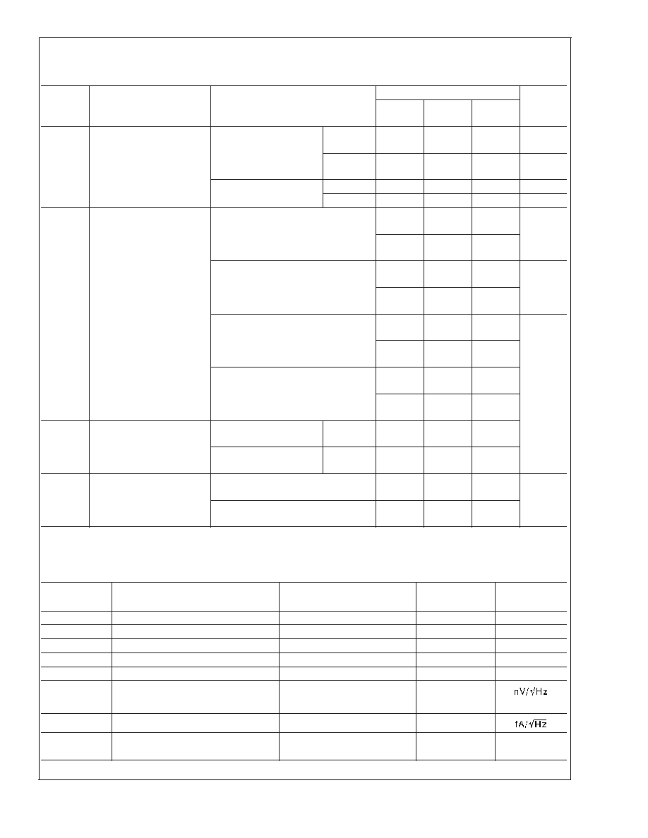
DC Electrical Characteristics
(Continued)
Unless otherwise specified, all limits guaranteed for T
J
= 25∞C, V
+
= 2.7V, V
-
= 0V, V
CM
= 1.0V, V
O
= 1.35V and R
L
>
1M
.
Boldface limits apply at the temperature extremes.
Symbol
Parameter
Conditions
LMC6035I/LMC6036I
Units
Min
(Note 6)
Typ
(Note 5)
Max
(Note 6)
A
V
Large Signal Voltage Gain
(Note 7)
R
L
= 600
Sourcing
100
75
1000
V/mV
Sinking
25
20
250
V/mV
R
L
= 2k
Sourcing
2000
V/mV
Sinking
500
V/mV
V
O
Output Swing
V
+
= 2.7V
R
L
= 600
to 1.35V
2.0
1.8
2.5
V
0.2
0.5
0.7
V
+
= 2.7V
R
L
= 2k
to 1.35V
2.4
2.2
2.62
V
0.07
0.2
0.4
V
+
= 15V
R
L
= 600
to 7.5V
13.5
13.0
14.5
V
0.36
1.25
1.50
V
+
= 15V,
R
L
= 2 k
to 7.5V
14.2
13.5
14.8
V
0.12
0.4
0.5
I
O
Output Current
V
O
= 0V
Sourcing
4
3
8
mA
V
O
= 2.7V
Sinking
3
2
5
I
S
Supply Current
LMC6035 for Both Amplifiers
V
O
= 1.35V
0.65
1.6
1.9
mA
LMC6036 for All Four Amplifiers
V
O
= 1.35V
1.3
2.7
3.0
AC Electrical Characteristics
Unless otherwise specified, all limits guaranteed for T
J
= 25∞C, V
+
= 2.7V, V
-
= 0V, V
CM
= 1.0V, V
O
= 1.35V and R
L
>
1 M
.
Boldface limits apply at the temperature extremes.
Symbol
Parameter
Conditions
Typ
Units
(Note 5)
SR
Slew Rate
(Note 9)
1.5
V/µs
GBW
Gain Bandwidth Product
V
+
= 15V
1.4
MHz
m
Phase Margin
48
∞
G
m
Gain Margin
17
dB
Amp-to-Amp Isolation
(Note 10)
130
dB
e
n
Input-Referred Voltage Noise
f = 1kHz
27
V
CM
= 1V
i
n
Input Referred Current Noise
f = 1kHz
0.2
THD
Total Harmonic Distortion
f = 10kHz, A
V
= -10
R
L
= 2k
, V
O
= 8 V
PP
0.01
%
LMC6035/LMC6036
www.national.com
3

AC Electrical Characteristics
(Continued)
Unless otherwise specified, all limits guaranteed for T
J
= 25∞C, V
+
= 2.7V, V
-
= 0V, V
CM
= 1.0V, V
O
= 1.35V and R
L
>
1 M
.
Boldface limits apply at the temperature extremes.
Symbol
Parameter
Conditions
Typ
Units
(Note 5)
V
+
= 10V
Note 1: Absolute Maximum Ratings indicate limits beyond which damage to the device may occur. Operating Ratings indicate conditions for which the device is
intended to be functional, but specific performance is not guaranteed. For guaranteed specifications and the test conditions, see the Electrical Characteristics.
Note 2: Human body model, 1.5k
in series with 100pF.
Note 3: Applies to both single-supply and split-supply operation. Continuous short circuit operation at elevated ambient temperature can result in exceeding the
maximum allowed junction temperature of 150∞C. Output currents in excess of 30mA over long term may adversely affect reliability.
Note 4: The maximum power dissipation is a function of T
J(MAX)
,
JA
, and T
A
. The maximum allowable power dissipation at any ambient temperature is
P
D
= (T
J(MAX)
-T
A
)/
JA
. All numbers apply for packages soldered directly onto a PC board with no air flow.
Note 5: Typical Values represent the most likely parametric norm or one sigma value.
Note 6: All limits are guaranteed by testing or statistical analysis.
Note 7: V
+
= 15V, V
CM
= 7.5V and R
L
connected to 7.5V. For Sourcing tests, 7.5V
V
O
11.5V. For Sinking tests, 3.5V V
O
7.5V.
Note 8: Do not short circuit output to V
+
when V
+
is greater than 13V or reliability will be adversely affected.
Note 9: V
+
= 15V. Connected as voltage follower with 10V step input. Number specified is the slower of the positive and negative slew rates.
Note 10: Input referred, V
+
= 15V and R
L
= 100k
connected to 7.5V. Each amp excited in turn with 1kHz to produce V
O
= 12 V
PP
.
Note 11: Guaranteed by design.
LMC6035/LMC6036
www.national.com
4
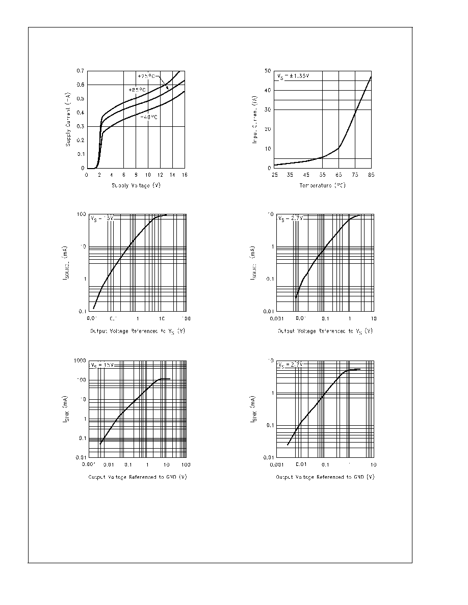
Typical Performance Characteristics
Unless otherwise specified, V
S
= 2.7V, single supply, T
A
=
25∞C
Supply Current vs. Supply Voltage (Per Amplifier)
Input Current vs. Temperature
01283052
01283053
Sourcing Current vs. Output Voltage
Sourcing Current vs. Output Voltage
01283054
01283055
Sinking Current vs. Output Voltage
Sinking Current vs. Output Voltage
01283056
01283057
LMC6035/LMC6036
www.national.com
5