 | ÐлекÑÑоннÑй компоненÑ: LM61 | СкаÑаÑÑ:  PDF PDF  ZIP ZIP |
Äîêóìåíòàöèÿ è îïèñàíèÿ www.docs.chipfind.ru
LM61
2.7V, SOT-23 or TO-92 Temperature Sensor
General Description
The LM61 is a precision integrated-circuit temperature sen-
sor that can sense a -30°C to +100°C temperature range
while operating from a single +2.7V supply. The LM61's out-
put voltage is linearly proportional to Celsius (Centigrade)
temperature (+10 mV/°C) and has a DC offset of +600 mV.
The offset allows reading negative temperatures without the
need for a negative supply. The nominal output voltage of the
LM61 ranges from +300 mV to +1600 mV for a -30°C to
+100°C temperature range. The LM61 is calibrated to pro-
vide accuracies of
±
2.0°C at room temperature and
±
3°C
over the full -25°C to +85°C temperature range.
The LM61's linear output, +600 mV offset, and factory cali-
bration simplify external circuitry required in a single supply
environment where reading negative temperatures is re-
quired. Because the LM61's quiescent current is less than
125 µA, self-heating is limited to a very low 0.2°C in still air.
Shutdown capability for the LM61 is intrinsic because its in-
herent low power consumption allows it to be powered di-
rectly from the output of many logic gates.
Features
n
Calibrated linear scale factor of +10 mV/°C
n
Rated for full -30° to +100°C range
n
Suitable for remote applications
Applications
n
Cellular Phones
n
Computers
n
Power Supply Modules
n
Battery Management
n
FAX Machines
n
Printers
n
HVAC
n
Disk Drives
n
Appliances
Key Specifications
n
Accuracy at 25°C
±
2.0 or
±
3.0°C
(max)
n
Accuracy for -30°C to +100°C
±
4.0°C (max)
n
Accuracy for -25°C to +85°C
±
3.0°C (max)
n
Temperature Slope
+10 mV/°C
n
Power Supply Voltage Range
+2.7V to +10V
n
Current Drain
@
25°C
125 µA (max)
n
Nonlinearity
±
0.8°C (max)
n
Output Impedance
800
(max)
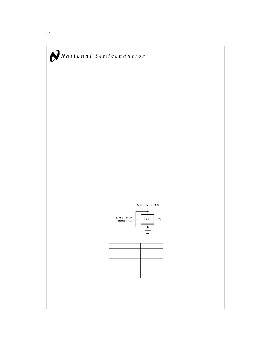
Typical Application
DS012897-2
V
O
= (+10 mV/°C x T °C) + 600 mV
Temperature (T)
Typical V
O
+100°C
+1600 mV
+85°C
+1450 mV
+25°C
+850 mV
0°C
+600 mV
-25°C
+350 mV
-30°C
+300 mV
FIGURE 1. Full-Range Centigrade Temperature Sensor (-30°C to +100°C)
Operating from a Single Li-Ion Battery Cell
June 1999
LM61
2.7V
,
SOT-23
or
T
O-92
T
emperature
Sensor
© 1999 National Semiconductor Corporation
DS012897
www.national.com
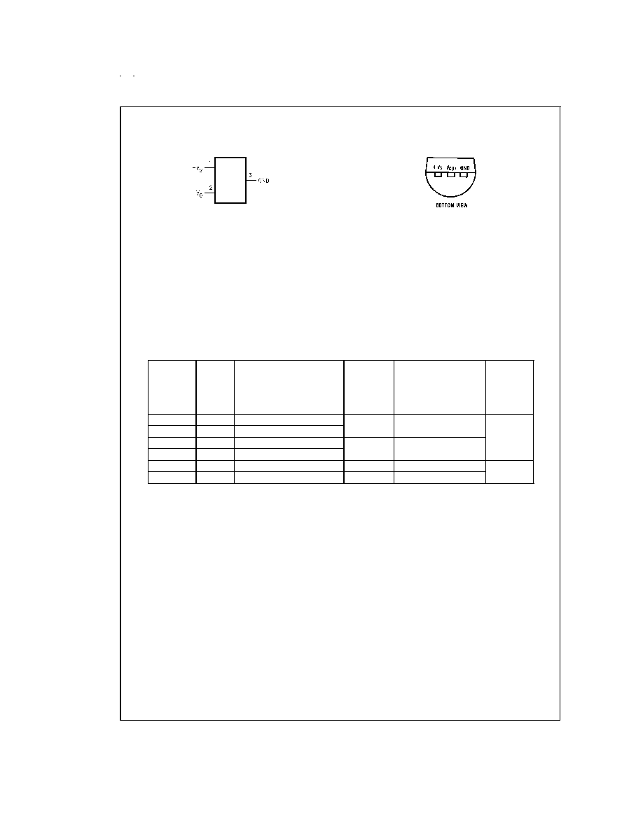
Connection Diagrams
Ordering Information
Order
Number
Device
Marking
Supplied In
Accuracy
Over
Specified
Temperature
Range (°C)
Specified
Temperature
Range
Package
Type
LM61BIM3
T1B
1000 Units on Tape and Reel
±
3
-25°C to +85°C
SOT-23
LM61BIM3X
T1B
3000 Units on Tape and Reel
LM61CIM3
T1C
1000 Units on Tape and Reel
±
4
-30°C to +100°C
LM61CIM3X
T1C
3000 Units on Tape and Reel
LM61BIZ
LM61BIZ
Bulk
±
3
-25°C to +85°C
TO-92
LM61CIZ
LM61CIZ
Bulk
±
4
-30°C to +100°C
SOT-23
DS012897-1
Top View
See NS Package Number MA03B
TO-92
DS012897-25
Top View
See NS Package Number Z03A
www.national.com
2
Absolute Maximum Ratings
(Note 1)
Supply Voltage
+12V to -0.2V
Output Voltage
(+V
S
+ 0.6V) to
-0.6V
Output Current
10 mA
Input Current at any pin (Note 2)
5 mA
Storage Temperature
-65°C to +150°C
Maximum Junction Temperature
(T
JMAX
)
+125°C
ESD Susceptibility (Note 3) :
Human Body Model
2500V
Machine Model
250V
Lead Temperature:
TO-92 Package:
Soldering (10 seconds)
+260°C
SOT-23 Package (Note 4):
Vapor Phase (60 seconds)
+215°C
Infrared (15 seconds)
+220°C
Operating Ratings
(Note 1)
Specified Temperature Range:
T
MIN
T
A
T
MAX
LM61C
-30°C
T
A
+100°C
LM61B
-25°C
T
A
+85°C
Supply Voltage Range (+V
S
)
+2.7V to +10V
Thermal Resistance,
JA
(Note 5)
SOT-23
TO-92
450°C/W
180°C/W
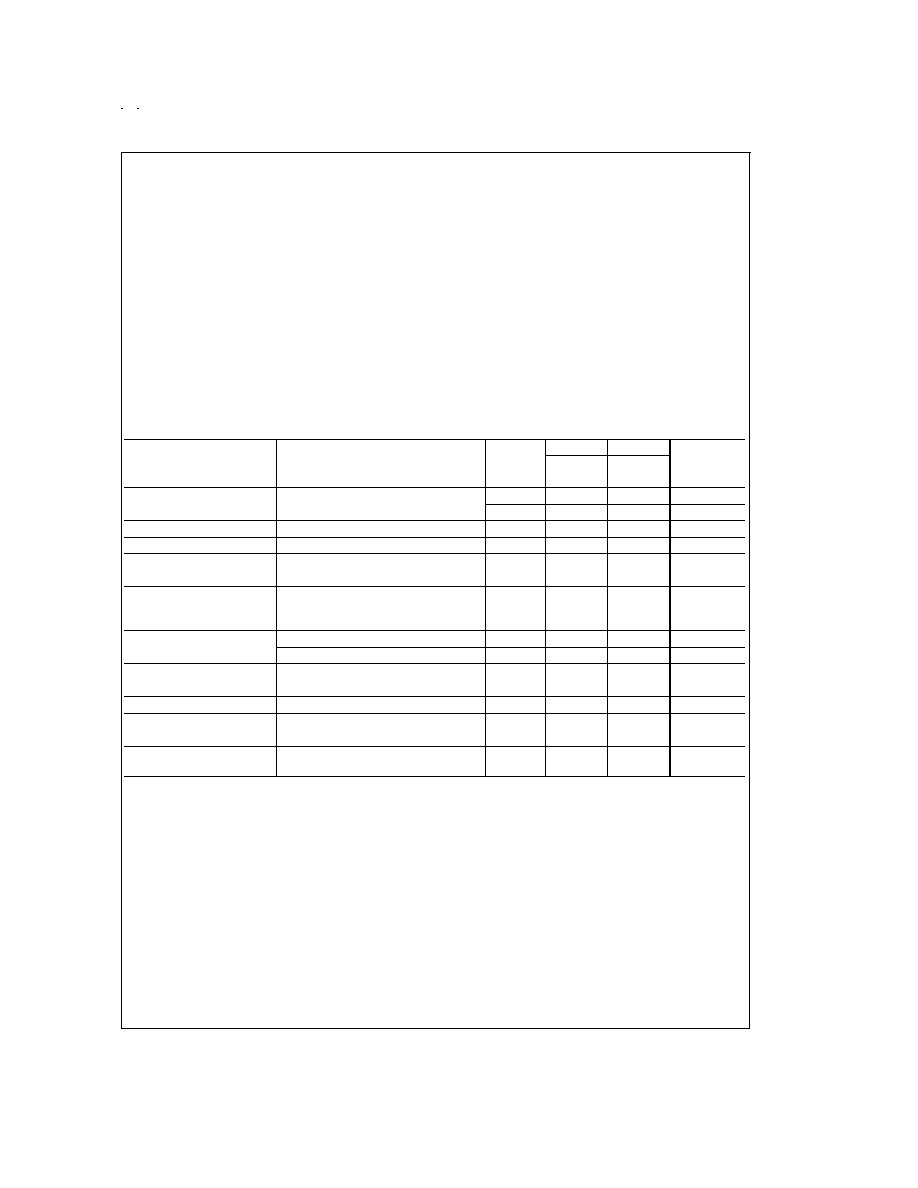
Electrical Characteristics
Unless otherwise noted, these specifications apply for +V
S
= +3.0 V
DC
. Boldface limits apply for T
A
= T
J
= T
MIN
to T
MAX
; all
other limits T
A
= T
J
= 25°C.
Parameter
Conditions
Typical
(Note 6)
LM61B
LM61C
Units
(Limit)
Limits
Limits
(Note 7)
(Note 7)
Accuracy (Note 8)
±
2.0
±
3.0
°C (max)
±
3.0
±
4.0
°C (max)
Output Voltage at 0°C
+600
mV
Nonlinearity (Note 9)
±
0.6
±
0.8
°C (max)
Sensor Gain
+10
+9.7
+9.6
mV/°C (min)
(Average Slope)
+10.3
+10.4
mV/°C (max)
Output Impedance
+3.0V
+V
S
+10V
-30°C
T
A
+85°C, +V
S
= +2.7V
+85°C
T
A
+100°C, +V
S
= +2.7V
0.8
2.3
5
0.8
2.3
5
k
(max)
k
(max)
k
(max)
Line Regulation (Note 10)
+3.0V
+V
S
+10V
±
0.7
±
0.7
mV/V (max)
+2.7V
+V
S
+3.3V
±
5.7
±
5.7
mV (max)
Quiescent Current
+2.7V
+V
S
+10V
82
125
125
µA (max)
155
155
µA (max)
Change of Quiescent Current
+2.7V
+V
S
+10V
±
5
µA
Temperature Coefficient of
0.2
µA/°C
Quiescent Current
Long Term Stability (Note 11)
T
J
=T
MAX
=+100°C,
for 1000 hours
±
0.2
°C
Note 1: Absolute Maximum Ratings indicate limits beyond which damage to the device may occur. Operating Ratings indicate conditions for which the device is func-
tional, but do not guarantee specific performance limits. For guaranteed specifications and test conditions, see the Electrical Characteristics. The guaranteed speci-
fications apply only for the test conditions listed. Some performance characteristics may degrade when the device is not operated under the listed test conditions.
Note 2: When the input voltage (V
I
) at any pin exceeds power supplies (V
I
<
GND or V
I
>
+V
S
), the current at that pin should be limited to 5 mA.
Note 3: The human body model is a 100 pF capacitor discharged through a 1.5 k
resistor into each pin. The machine model is a 200 pF capacitor discharged di-
rectly into each pin.
Note 4: See AN-450 "Surface Mounting Methods and Their Effect on Product Reliability" or the section titled "Surface Mount" found in any post 1986 National Semi-
conductor Linear Data Book for other methods of soldering surface mount devices.
Note 5: The junction to ambient thermal resistance (
JA
) is specified without a heat sink in still air.
Note 6: Typicals are at T
J
= T
A
= 25°C and represent most likely parametric norm.
Note 7: Limits are guaranteed to National's AOQL (Average Outgoing Quality Level).
Note 8: Accuracy is defined as the error between the output voltage and +10 mV/°C times the device's case temperature plus 600 mV, at specified conditions of volt-
age, current, and temperature (expressed in °C).
Note 9: Nonlinearity is defined as the deviation of the output-voltage-versus-temperature curve from the best-fit straight line, over the device's rated temperature
range.
Note 10: Regulation is measured at constant junction temperature, using pulse testing with a low duty cycle. Changes in output due to heating effects can be com-
puted by multiplying the internal dissipation by the thermal resistance.
Note 11: For best long-term stability, any precision circuit will give best results if the unit is aged at a warm temperature, and/or temperature cycled for at least 46
hours before long-term life test begins. This is especially true when a small (Surface-Mount) part is wave-soldered; allow time for stress relaxation to occur. The ma-
jority of the drift will occur in the first 1000 hours at elevated temperatures. The drift after 1000 hours will not continue at the first 1000 hour rate.
www.national.com
3
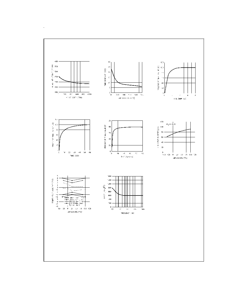
Typical Performance Characteristics
The LM61 in the SOT-23 package mounted to a printed circuit
board as shown in
Figure 2 was used to generate the following thermal curves.
Thermal Resistance
Junction to Air
DS012897-3
Thermal Time Constant
DS012897-4
Thermal Response in
Still Air with Heat Sink
DS012897-5
Thermal Response
in Stirred Oil Bath
with Heat Sink
DS012897-6
Thermal Response in Still
Air without a Heat Sink
DS012897-8
Quiescent Current
vs. Temperature
DS012897-9
Accuracy vs Temperature
DS012897-10
Noise Voltage
DS012897-11
www.national.com
4
Typical Performance Characteristics
The LM61 in the SOT-23 package mounted to a printed
circuit board as shown in
Figure 2 was used to generate the following thermal curves. (Continued)
1.0 Mounting
The LM61 can be applied easily in the same way as other
integrated-circuit temperature sensors. It can be glued or ce-
mented to a surface. The temperature that the LM61 is sens-
ing will be within about +0.2°C of the surface temperature
that LM61's leads are attached to.
This presumes that the ambient air temperature is almost the
same as the surface temperature; if the air temperature were
much higher or lower than the surface temperature, the ac-
tual temperature measured would be at an intermediate tem-
perature between the surface temperature and the air tem-
perature.
To ensure good thermal conductivity the backside of the
LM61 die is directly attached to the GND pin. The lands and
traces to the LM61 will, of course, be part of the printed cir-
cuit board, which is the object whose temperature is being
measured.
Alternatively, the LM61 can be mounted inside a sealed-end
metal tube, and can then be dipped into a bath or screwed
into a threaded hole in a tank. As with any IC, the LM61 and
accompanying wiring and circuits must be kept insulated and
dry, to avoid leakage and corrosion. This is especially true if
the circuit may operate at cold temperatures where conden-
sation can occur. Printed-circuit coatings and varnishes such
as Humiseal and epoxy paints or dips are often used to en-
sure that moisture cannot corrode the LM61 or its connec-
tions.
The thermal resistance junction to ambient (
JA
) is the pa-
rameter used to calculate the rise of a device junction tem-
perature due to its power dissipation. For the LM61 the
equation used to calculate the rise in the die temperature is
as follows:
T
J
= T
A
+
JA
[(+V
S
I
Q
) + (+V
S
- V
O
) I
L
]
where I
Q
is the quiescent current and I
L
is the load current on
the output. Since the LM61's junction temperature is the ac-
tual temperature being measured care should be taken to
minimize the load current that the LM61 is required to drive.
The table shown in
Figure 3 summarizes the rise in die tem-
perature of the LM61 without any loading with a 3.3V supply,
and the thermal resistance for different conditions.
Supply Voltage
vs Supply Current
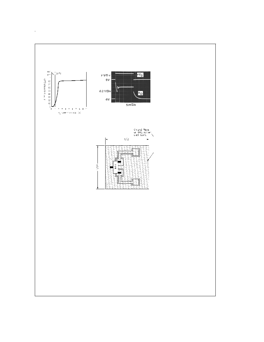
DS012897-12
Start-Up Response
DS012897-22
DS012897-14
FIGURE 2. Printed Circuit Board Used
for Heat Sink to Generate All Curves.
1
/
2
" Square Printed Circuit Board
with 2 oz. Copper Foil or Similar.
www.national.com
5