TL H 11058
LM612
Dual-Channel
Comparator
and
Reference
February 1995
LM612
Dual-Channel Comparator and Reference
General Description
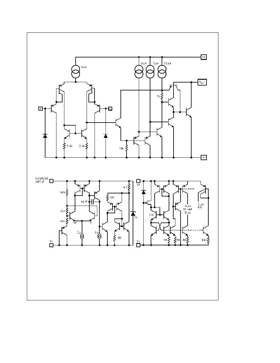
The dual-channel comparator consists of two individual
comparators having an input voltage range that extends
down to the negative supply voltage V
b
The common
open-collector output can be driven low by either half of the
LM612 This configuration makes the LM612 ideal for use
as a window comparator The input stages of the compara-
tor have lateral PNP input transistors which maintain low
input currents for large differential input voltages and swings
above V
a
The 1 2V voltage reference referred to the V
b
terminal is a
two-terminal shunt-type band-gap similar to the LM185-1 2
series with voltage accuracy of
g
0 6% available The refer-
ence features operation over a shunt current range of 17 mA
to 20 mA low dynamic impedance and broad capacitive
load range
As a member of National's Super-Block
TM
family
the
LM612 is a space-saving monolithic alternative to a multi-
chip solution offering a high level of integration without sac-
rificing performance
Features
COMPARATORS
Y
Low operating current
300 mA
Y
Wide supply voltage range
4V to 36V
Y
Open-collector outputs
Y
Input common-mode range
V
b
to (V
a
b
1 8V)
Y
Wide differential input voltage
g
36V
REFERENCE
Y
Fixed output voltage
1 24V
Y
Tight initial tolerance available
g
0 6% (25 C)
Y
Wide operating current range
17 mA to 20 mA
Y
Tolerant of load capacitance
Applications
Y
Voltage window comparator
Y
Power supply voltage monitor
Y
Dual-channel fault monitor
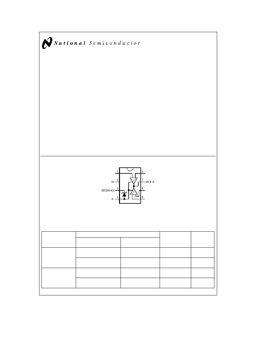
Connection Diagram
TL H 11058 ≠ 1
Top View
Ordering Information
For information about surface-mount packaging of this device please contact the Analog Product Marketing group at
National Semiconductor Corporation headquarters
Tolerances
Reference
Temperature Range
Package
Package
Number
NSC
Military
Industrial
b
55 C
s
T
J
s
a
125 C
b
40 C
s
T
J
a
85 C
g
0 6% at 25 C
LM612AMN
LM612AIN
8-Pin
N08E
80 ppm C Max
Molded DIP
LM612AMJ 883
8-Pin
J08A
(Note 13)
Ceramic DIP
g
2 0% at 25 C
LM612MN
LM612IN
8-Pin
N08E
150 ppm C Max
Molded DIP
LM612IM
8-Pin Narrow
M08A
Surface Mount
Super-Block
TM
is a trademark of National Semiconductor Corporation
C1995 National Semiconductor Corporation
RRD-B30M115 Printed in U S A
Absolute Maximum Ratings
(Note 1)
If Military Aerospace specified devices are required
please contact the National Semiconductor Sales
Office Distributors for availability and specifications
Voltage on Any Pin Except V
R
(referred to V
b
pin)
(Note 2)
36V (Max)
(Note 3)
b
0 3V (Min)
Current through Any Input Pin and V
R
Pin
g
20 mA
Differential Input Voltage
g
36V
Output Short-Circuit Duration
(Note 4)
Storage Temperature Range
b
65 C
s
T
J
s
a
150 C
Maximum Junction Temperature
150 C
Thermal Resistance Junction-to-Ambient (Note 5)
N Package
100 C W
Soldering Information
N Package
Soldering (10 seconds)
260 C
ESD Tolerance (Note 6)
g
1 kV
Operating Temperature Range
LM612AI LM612I
b
40 C
s
T
J
s
a
85 C
LM612AM LM612M
b
55 C
s
T
J
s
a
125 C
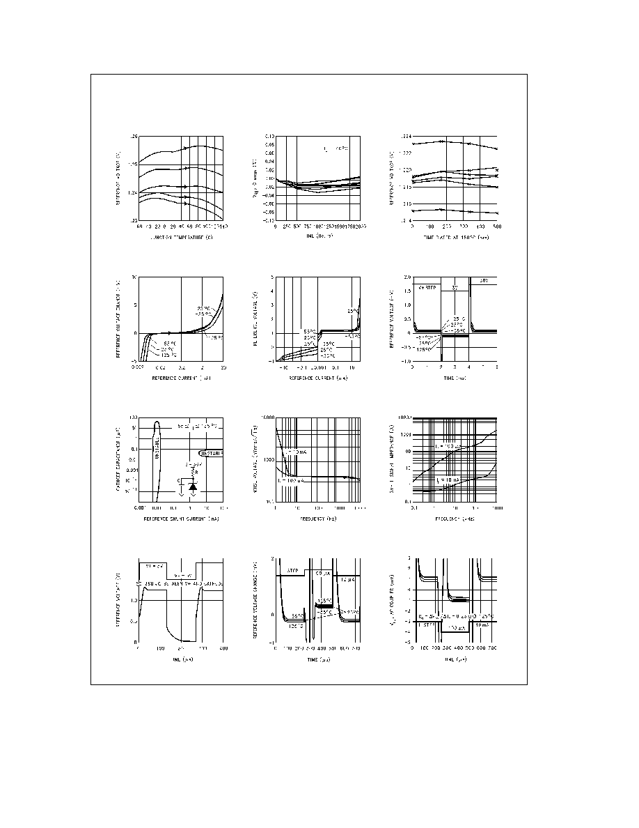
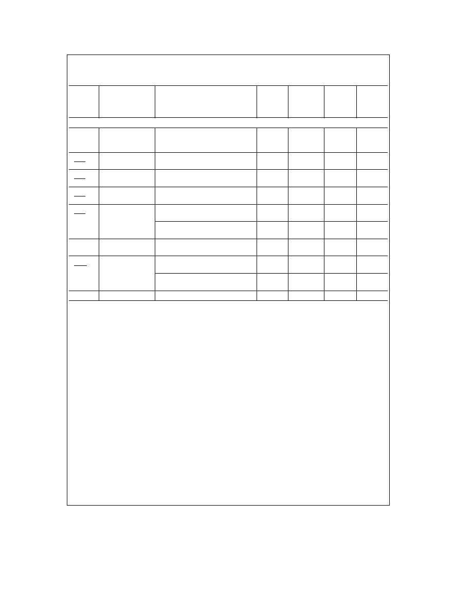
Electrical Characteristics
These specifications apply for V
b
e
GND
e
0V V
a
e
5V V
CM
e
V
OUT
e
V
a
2
I
R
e
100 mA unless otherwise specified Limits in standard typeface are for T
J
e
25 C limits in boldface type apply over the
Operating Temperature Range
Symbol
Parameter
Conditions
(Note 7)
Typical
LM612AM
LM612M
Units
LM612AI
LM612I
Limits
Limits
(Note 8)
(Note 8)
COMPARATORS
I
S
Total Supply Current
V
a
Current R
LOAD
e
%
150
250
250
m
A Max
3V
s
V
a s
36V
170
300
300
m
A Max
V
OS
Offset Voltage over
4V
s
V
a s
36V R
L
e
15 kX
1 0
3 0
5 0
mV Max
V
a
Range
2 0
6 0
7 0
mV Max
V
OS
Offset Voltage over
0V
s
V
CM
s
(V
a
b
1 8V)
1 0
3 0
5 0
mV Max
V
CM
Range
V
a
e
30V R
L
e
15 kX
1 5
6 0
7 0
mV Max
D
V
OS
D
T
Average Offset Voltage
15
m
V C
Drift
I
B
Input Bias Current
5
25
35
nA Max
8
30
40
nA Max
I
OS
Input Offset Current
0 2
4
4
nA Max
0 3
5
5
nA Max
A
V
Voltage Gain
R
L
e
10 kX to 36V
500
50
50
V mV Min
2V
s
V
OUT
s
27V
100
V mV
t
R
Large Signal Response
V
a
IN
e
1 4V V
b
IN
e
TTL
1 5
m
s
Time
Swing R
L
e
5 1 kX
2 0
m
s
I
SINK
Output Sink Current
V
a
IN
e
0V V
b
IN
e
1V
20
10
10
mA Min
V
OUT
e
1 5V
13
8
8
mA Min
V
OUT
e
0 4V
2 8
1 0
0 8
mA Min
2 4
0 5
0 5
mA Min
I
L
Output Leakage Current
V
a
IN
e
1V V
b
IN
e
0V
0 1
10
10
m
A Max
V
OUT
e
36V
0 2
m
A
2
Electrical Characteristics
These specifications apply for V
b
e
GND
e
0V V
a
e
5V V
CM
e
V
OUT
e
V
a
2
I
R
e
100 mA unless otherwise specified Limits in standard typeface are for T
J
e
25 C limits in boldface type apply over the
Operating Temperature Range
(Continued)
Symbol
Parameter
Conditions
(Note 7)
Typical
LM612AM
LM612M
Units
LM612AI
LM612I
Limits
Limits
(Note 8)
(Note 8)
VOLTAGE REFERENCE
(Note 9)
V
R
Reference Voltage
1 244
1 2365
1 2191
V Min
1 2515
1 2689
V Max
(
g
0 6%)
(
g
2%)
D
V
R
D
T
Average Drift with
(Note 10)
18
80
150
ppm C
Temperature
Max
D
V
R
kH
Average Drift with
T
J
e
40 C
400
ppm kH
Time
T
J
e
150 C
1000
ppm kH
D
V
R
D
T
J
Hysteresis
(Note 11)
3 2
m
V C
D
V
R
D
I
R
V
R
Change with
V
R 100 mA
b
V
R 17 mA
0 05
1
1
mV Max
Current
0 1
1 1
1 1
mV Max
V
R 10 mA
b
V
R 100 mA
1 5
5
5
mV Max
(Note 12)
2 0
5 5
5 5
mV Max
R
Resistance
D
V
R 10 mA to 0 1 mA
9 9 mA
0 2
0 56
0 56
X
Max
D
V
R 100 mA to 17 mA
83 mA
0 6
13
13
X
Max
D
V
R
D
V
a
V
R
Change with
V
R Va e 5V
b
V
R Va e 36V
0 1
1 2
1 2
mV Max
V
a
Change
0 1
1 3
1 3
mV Max
V
R Va e 5V
b
V
R Va e 3V
0 01
1
1
mV Max
0 01
1 5
1 5
mV Max
e
n
Voltage Noise
BW
e
10 Hz to 10 kHz
30
m
V
RMS
Note 1
Absolute maximum ratings indicate limits beyond which damage to the component may occur Electrical specifications do not apply when operating the
device beyond its rated operating conditions
Note 2
Input voltage above V
a
is not allowed As long as one input pin voltage remains inside the common-mode range the comparator will deliver the correct
output
Note 3
More accurately it is excessive current flow with resulting excess heating that limits the voltages on all pins When any pin is pulled a diode drop below
V
b
a parasitic NPN transistor turns ON No latch-up will occur as long as the current through that pin remains below the Maximum Rating Operation is undefined
and unpredictable when any parasitic diode or transistor is conducting
Note 4
Shorting the Output to V
b
will not cause power dissipation so it may be continuous However shorting the Output to any more positive voltage (including
V
a
) will cause 80 mA (typ ) to be drawn through the output transistor This current multiplied by the applied voltage is the power dissipation in the output transistor
If this total power causes the junction temperature to exceed 150 C degraded reliability or destruction of the device may occur To determine junction temperature
see Note 5
Note 5
Junction temperature may be calculated using T
J
e
T
A
a
P
D
i
JA
The given thermal resistance is worst-case for packages in sockets in still air For
packages soldered to copper-clad board with dissipation from one comparator or reference output transistor nominal i
JA
is 90 C W for the N package
Note 6
Human body model 100 pF discharged through a 1 5 kX resistor
Note 7
Typical values in standard typeface are for T
J
e
25 C values in boldface type apply for the full operating temperature range These values represent the
most likely parametric norm
Note 8
All limits are guaranteed for T
J
e
25 C (standard type face) or over the full operating temperature range (bold type face)
Note 9
V
R
is the reference output voltage nominally 1 24V
Note 10
Average reference drift is calculated from the measurement of the reference voltage at 25 C and at the temperature extremes The drift in ppm C is
10
6
D
V
R
V
R 25 C
D
T
J
where DV
R
is the lowest value subtracted from the highest V
R 25 C
is the value at 25 C and DT
J
is the temperature range This
parameter is guaranteed by design and sample testing
Note 11
Hysteresis is the change in V
R
caused by a change in T
J
after the reference has been ``dehysterized'' To dehysterize the reference that is minimize the
hysteresis to the typical value its junction temperature should be cycled in the following pattern spiralling in toward 25 C 25 C 85 C
b
40 C 70 C 0 C 25 C
Note 12
Low contact resistance is required for accurate measurement
Note 13
A military RETS 612AMX electrical test specification is available on request The military screened parts can also be procured as a Standard Military
Drawing
3