 | –≠–ª–µ–∫—Ç—Ä–æ–Ω–Ω—ã–π –∫–æ–º–ø–æ–Ω–µ–Ω—Ç: LM6134AI | –°–∫–∞—á–∞—Ç—å:  PDF PDF  ZIP ZIP |
LM6132 /LM6134
Dual and Quad Low Power 10 MHz Rail-to-Rail I/O
Operational Amplifiers
General Description
The LM6132/34 provides new levels of speed vs power per-
formance in applications where low voltage supplies or
power limitations previously made compromise necessary.
With
only
360 µA/amp
supply
current,
the
10
MHz
gain-bandwidth of this device supports new portable applica-
tions where higher power devices unacceptably drain battery
life.
The LM6132/34 can be driven by voltages that exceed both
power supply rails, thus eliminating concerns over exceeding
the common-mode voltage range. The rail-to-rail output
swing capability provides the maximum possible dynamic
range at the output. This is particularly important when oper-
ating on low supply voltages. The LM6132/34 can also drive
large capacitive loads without oscillating.
Operating on supplies from 2.7V to over 24V, the LM6132/34
is excellent for a very wide range of applications, from bat-
tery operated systems with large bandwidth requirements to
high speed instrumentation.
Features
(For 5V Supply, Typ Unless Noted)
n
Rail-to-Rail input CMVR -0.25V to 5.25V
n
Rail-to-Rail output swing 0.01V to 4.99V
n
High gain-bandwidth, 10 MHz at 20 kHz
n
Slew rate 12 V/µs
n
Low supply current 360 µA/Amp
n
Wide supply range 2.7V to over 24V
n
CMRR 100 dB
n
Gain 100 dB with R
L
= 10k
n
PSRR 82 dB
Applications
n
Battery operated instrumentation
n
Instrumentation Amplifiers
n
Portable scanners
n
Wireless communications
n
Flat panel display driver
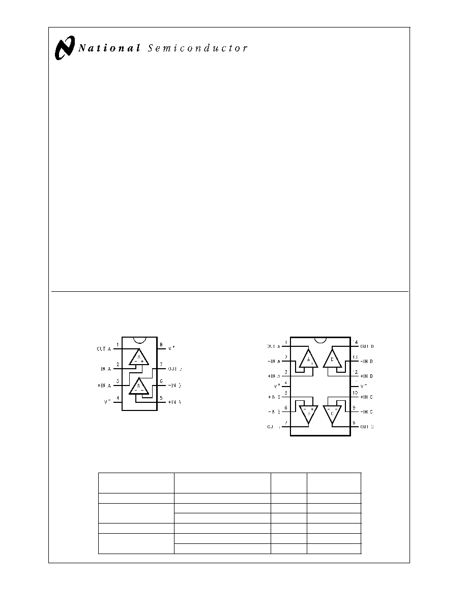
Connection Diagrams
Ordering Information
Package
Temperature Range
NSC
Transport
Industrial, -40∞C to +85∞C
Drawing
Media
8-Pin Molded DIP
LM6132AIN, LM6132BIN
N08E
Rails
8-Pin Small Outline
LM6132AIM, LM6132BIM
M08A
Rails
LM6132AIMX, LM6132BIMX
M08A
Tape and Reel
14-Pin Molded DIP
LM6134AIN, LM6134BIN
N14A
Rails
14-Pin Small Outline
LM6134AIM, LM6134BIM
M14A
Rails
LM6134AIMX, LM6134BIMX
M14A
Tape and Reel
8-Pin DIP/SO
DS012349-1
Top View
14-Pin DIP/SO
DS012349-2
Top View
August 2000
LM6132
and
LM6134
Dual
and
Quad,
Low
Power
10
MHz
Rail-to-Rail
I/O
Operational
Amplifiers
© 2000 National Semiconductor Corporation
DS012349
www.national.com
Absolute Maximum Ratings
(Note 1)
If Military/Aerospace specified devices are required,
please contact the National Semiconductor Sales Office/
Distributors for availability and specifications.
ESD Tolerance (Note 2)
2500V
Differential Input Voltage
15V
Voltage at Input/Output Pin
(V
+
)+0.3V, (V
-
)-0.3V
Supply Voltage (V
+
≠V
-
)
35V
Current at Input Pin
±
10 mA
Current at Output Pin (Note 3)
±
25 mA
Current at Power Supply Pin
50 mA
Lead Temp. (soldering, 10 sec.)
260∞C
Storage Temperature Range
-65∞C to +150∞C
Junction Temperature (Note 4)
150∞C
Operating Ratings
(Note 1)
Supply Voltage
1.8V
V
S
24V
Junction Temperature Range
LM6132, LM6134
-40∞C
T
J
+85∞C
Thermal resistance (
JA
)
N Package, 8-pin Molded DIP
115∞C/W
M Package, 8-pin Surface Mount
193∞C/W
N Package, 14-pin Molded DIP
81∞C/W
M Package, 14-pin Surface Mount
126∞C/W
5.0V DC Electrical Characteristics
Unless otherwise specified, all limits guaranteed for T
J
= 25∞C, V
+
= 5.0V, V
-
= 0V, V
CM
= V
O
= V
+
/2 and R
L
>
1 M
to V
S
/2.
Boldface limits apply at the temperature extremes
Symbol
Parameter
Conditions
Typ
(Note 5)
LM6134AI
LM6134BI
Units
LM6132AI
LM6132BI
Limit
Limit
(Note 6)
(Note 6)
V
OS
Input Offset Voltage
0.25
2
4
6
8
mV
max
TCV
OS
Input Offset Voltage Average Drift
5
µV/C
I
B
Input Bias Current
0V
V
CM
5V
110
140
300
180
350
nA
max
I
OS
Input Offset Current
3.4
30
50
30
50
nA
max
R
IN
Input Resistance, CM
104
M
CMRR
Common Mode Rejection Ratio
0V
V
CM
4V
100
75
70
75
70
dB
min
0V
V
CM
5V
80
60
55
60
55
PSRR
Power Supply Rejection Ratio
±
2.5V
V
S
±
12V
82
78
75
78
75
dB
min
V
CM
Input Common-Mode Voltage
Range
-0.25
0
0
V
5.25
5.0
5.0
A
V
Large Signal Voltage Gain
R
L
= 10k
100
25
8
15
6
V/mV
min
V
O
Output Swing
100k Load
4.992
4.98
4.93
4.98
4.93
V
min
0.007
0.017
0.019
0.017
0.019
V
max
10k Load
4.952
4.94
4.85
4.94
4.85
V
min
0.032
0.07
0.09
0.07
0.09
V
max
5k Load
4.923
4.90
4.85
4.90
4.85
V
min
0.051
0.095
0.12
0.095
0.12
V
max
I
SC
Output Short Circuit Current
LM6132
Sourcing
4
2
2
2
1
mA
min
Sinking
3.5
1.8
1.8
1.8
1
mA
min
LM6132/LM6134
www.national.com
2
5.0V DC Electrical Characteristics
(Continued)
Unless otherwise specified, all limits guaranteed for T
J
= 25∞C, V
+
= 5.0V, V
-
= 0V, V
CM
= V
O
= V
+
/2 and R
L
>
1 M
to V
S
/2.
Boldface limits apply at the temperature extremes
Symbol
Parameter
Conditions
Typ
(Note 5)
LM6134AI
LM6134BI
Units
LM6132AI
LM6132BI
Limit
Limit
(Note 6)
(Note 6)
I
SC
Output Short Circuit Current
LM6134
Sourcing
3
2
1.6
2
1
mA
min
Sinking
3.5
1.8
1.3
1.8
1
mA
min
I
S
Supply Current
Per Amplifier
360
400
450
400
450
µA
max
5.0V AC Electrical Characteristics
Unless otherwise specified, all limits guaranteed for T
J
= 25∞C, V
+
= 5.0V, V
-
= 0V, V
CM
= V
O
= V
+
/2 and R
L
>
1 M
to V
S
/2.
Boldface limits apply at the temperature extremes
Symbol
Parameter
Conditions
Typ
(Note 5)
LM6134AI
LM6134BI
Units
LM6132AI
LM6132BI
Limit
Limit
(Note 6)
(Note 6)
SR
Slew Rate
±
4V
@
V
S
=
±
6V
14
8
8
V/µs
R
S
<
1 k
7
7
min
GBW
Gain-Bandwidth Product
f = 20 kHz
10
7.4
7.4
MHz
7
7
min
m
Phase Margin
R
L
= 10k
33
deg
G
m
Gain Margin
R
L
= 10k
10
dB
e
n
Input Referred Voltage Noise
f = 1 kHz
27
i
n
Input Referred Current Noise
f = 1 kHz
0.18
2.7V DC Electrical Characteristics
Unless otherwise specified, all limits guaranteed for T
J
= 25∞C, V
+
= 2.7V, V
-
= 0V, V
CM
= V
O
= V
+
/2 and R
L
>
1 M
to V
S
/2.
Boldface limits apply at the temperature extreme
Symbol
Parameter
Conditions
Typ
(Note 5)
LM6134AI
LM6134BI
Units
LM6132AI
LM6132BI
Limit
Limit
(Note 6)
(Note 6)
V
OS
Input Offset Voltage
0.12
2
6
mV
8
12
max
I
B
Input Bias Current
0V
V
CM
2.7V
90
nA
I
OS
Input Offset Current
2.8
nA
R
IN
Input Resistance
134
M
CMRR
Common Mode
0V
V
CM
2.7V
82
dB
Rejection Ratio
PSRR
Power Supply
±
1.35V
V
S
±
12V
80
dB
Rejection Ratio
V
CM
Input Common-Mode
2.7
2.7
V
Voltage Range
0
0
A
V
Large Signal
R
L
= 10k
100
V/mV
LM6132/LM6134
www.national.com
3
2.7V DC Electrical Characteristics
(Continued)
Unless otherwise specified, all limits guaranteed for T
J
= 25∞C, V
+
= 2.7V, V
-
= 0V, V
CM
= V
O
= V
+
/2 and R
L
>
1 M
to V
S
/2.
Boldface limits apply at the temperature extreme
Symbol
Parameter
Conditions
Typ
(Note 5)
LM6134AI
LM6134BI
Units
LM6132AI
LM6132BI
Limit
Limit
(Note 6)
(Note 6)
Voltage Gain
V
O
Output Swing
R
L
= 100k
0.03
0.08
0.08
V
0.112
0.112
max
2.66
2.65
2.65
V
2.25
2.25
min
I
S
Supply Current
Per Amplifier
330
µA
2.7V AC Electrical Characteristics
Unless otherwise specified, all limits guaranteed for T
J
= 25∞C, V
+
= 2.7V, V
-
= 0V, V
CM
= V
O
= V
+
/2 and R
L
>
1 M
to V
S
/2.
Symbol
Parameter
Conditions
Typ
(Note 5)
LM6134AI
LM6134BI
Units
LM6132AI
LM6132BI
Limit
Limit
(Note 6)
(Note 6)
GBW
Gain-Bandwidth Product
R
L
= 10k, f = 20 kHz
7
MHz
m
Phase Margin
R
L
= 10k
23
deg
G
m
Gain Margin
12
dB
LM6132/LM6134
www.national.com
4
24V DC Electrical Characteristics
Unless otherwise specified, all limits guaranteed for T
J
= 25∞C, V
+
= 24V, V
-
= 0V, V
CM
= V
O
= V
+
/2 and R
L
>
1 M
to V
S
/2.
Boldface limits apply at the temperature extreme
Symbol
Parameter
Conditions
Typ
(Note 5)
LM6134AI
LM6134BI
Units
LM6132AI
LM6132BI
Limit
Limit
(Note 6)
(Note 6)
V
OS
Input Offset Voltage
1.7
3
7
mV
5
9
max
I
B
Input Bias Current
0V
V
CM
24V
125
nA
I
OS
Input Offset Current
4.8
nA
R
IN
Input Resistance
210
M
CMRR
Common Mode
0V
V
CM
24V
80
dB
Rejection Ratio
PSRR
Power Supply
2.7V
V
S
24V
82
dB
Rejection Ratio
V
CM
Input Common-Mode
-0.25
0
0
V min
Voltage Range
24.25
24
24
V max
A
V
Large Signal
R
L
= 10k
102
V/mV
Voltage Gain
V
O
Output Swing
R
L
= 10k
0.075
0.15
0.15
V
max
23.86
23.8
23.8
V
min
I
S
Supply Current
Per Amplifier
390
450
450
µA
490
490
max
24V AC Electrical Characteristics
Unless otherwise specified, all limits guaranteed for T
J
= 25∞C, V
+
= 24V, V
-
= 0V, V
CM
= V
O
= V
+
/2 and R
L
>
1 M
to V
S
/2.
Symbol
Parameter
Conditions
Typ
(Note 5)
LM6134AI
LM6134BI
Units
LM6132AI
LM6132BI
Limit
Limit
(Note 6)
(Note 6)
GBW
Gain-Bandwidth Product
R
L
= 10k, f = 20 kHz
11
MHz
m
Phase Margin
R
L
= 10k
23
deg
G
m
Gain Margin
R
L
= 10k
12
dB
THD +
N
Total Harmonic
A
V
= +1, V
O
= 20V
P-P
0.0015
%
Distortion and Noise
f = 10 kHz
Note 1: Absolute Maximum Ratings indicate limits beyond which damage to the device may occur. Operating Ratings indicate conditions for which the device is in-
tended to be functional, but specific performance is not guaranteed. For guaranteed specifications and the test conditions, see the Electrical characteristics.
Note 2: Human body model, 1.5 k
in series with 100 pF.
Note 3: Applies to both single-supply and split-supply operation. Continuous short circuit operation at elevated ambient temperature can result in exceeding the
maximum allowed junction temperature of 150∞C.
Note 4: The maximum power dissipation is a function of T
J(max)
,
JA
, and T
A
. The maximum allowable power dissipation at any ambient temperature is P
D
= (T
J(max)
- T
A
)/
JA
. All numbers apply for packages soldered directly into a PC board.
Note 5: Typical Values represent the most likely parametric norm.
Note 6: All limits are guaranteed by testing or statistical analysis.
LM6132/LM6134
www.national.com
5